8. System configuration controller (SYSCFG) and routing interface (RI)
This section applies to the whole STM32L1xxxx family, unless otherwise specified.
8.1 SYSCFG and RI introduction
The system configuration controller is mainly used to remap the memory accessible in the code area, and manage the external interrupt line connection to the GPIOs.
The routing interface provides high flexibility by allowing the software routing of I/Os toward the input captures of the STM32L1xxxx three general-purpose timers (TIM2, TIM3 and TIM4).
The STM32L1xxxx ADC has an analog input matrix that is usually managed by a specific ADC interface. With the routing interface, it is possible to connect several I/O analog pins to a given channel of the ADC matrix by managing the analog switches of each I/O.
8.2 RI main features
- • TIM2/TIM3/TIM4's input captures 1,2,3 and four routing selections from selectable I/Os
- • Routing of internal reference voltage \( V_{REFINT} \) to selectable I/Os for all packages
- • Up to 40 external I/Os + 3 internal nodes (internal reference voltage + temperature sensor + \( V_{DD} \) and \( V_{DD/2} \) measurement by \( V_{COMP} \) ) can be used for data acquisition purposes in conjunction with the ADC interface
- • Input and output routing of COMP1 and COMP2
Note: The RI registers can be accessed only when the comparator interface clock is enabled by setting the COMPEN bit in the RCC_APB1ENR register. Refer to Section 6.3.10 on page 157 .
Figure 25. Routing interface (RI) block diagram for Cat.1 and Cat.2 devices
The diagram illustrates the internal routing interface (RI) for Cat.1 and Cat.2 devices. It shows how various I/O pins are connected to internal functional blocks through a series of switches and multiplexers.
- ADC Switch Matrix:
A central matrix that routes signals to the ADC. Inputs include:
- Group 2: PA6 (ADC_IN6), PA7 (ADC_IN7)
- Group 8: PC0 (ADC_IN10), PC1 (ADC_IN11), PC2 (ADC_IN12), PC3 (ADC_IN13)
- Group 1: PA0 (ADC_IN0), PA1 (ADC_IN1), PA2 (ADC_IN2), PA3 (ADC_IN3)
- Group 9: PC4 (ADC_IN14), PC5 (ADC_IN15)
- Group 7: PB12 (ADC_IN18), PB13 (ADC_IN19), PB14 (ADC_IN20), PB15 (ADC_IN21)
- Group 3: PB0 (ADC_IN8), PB1 (ADC_IN9)
- Group 6: PB4 (GR6-1), PB5 (GR6-2)
- Group 10: PC6 (GR10-1), PC7 (GR10-2), PC8 (GR10-3), PC9 (GR10-4)
- Group 4: PA8 (GR4-1), PA9 (GR4-2), PA10 (GR4-3)
- Group 5: PA13 (GR5-1), PA14 (GR5-2), PA15 (GR5-3)
- Direct connections: PA4 (ADC_IN4), PA5 (ADC_IN5), PE7 (ADC_IN22), PE8 (ADC_IN23), PE9 (ADC_IN24), PE10 (ADC_IN25)
- Internal sources: Temp. sensor (ADC_IN16), V REFINT (ADC_IN17), V COMP (ADC_IN26)
- COMP1 (Comparator 1): Receives inputs from V DD and GND through a network of 10 kΩ and 400 kΩ resistors and switches. Its non-inverting input (+) is connected to V REFINT .
- COMP2 (Comparator 2): Receives inputs from DAC_OUT1, DAC_OUT2, and V REFOUTEN (via a buffer). Its non-inverting input (+) is connected to V REFINT .
- OUTSEL[2:0] bits: A control block that selects signals for TIM2 input capture 4, TIM2 OREF clear, TIM3 input capture 4, TIM3 OREF clear, TIM4 input capture 4, TIM4 OREF clear, and TIM10 input capture 1.
- V REFINT Buffer: A buffer that provides a stable reference voltage (~1.2V) to the ADC and comparators. It has selectable output levels: V REFINT ~1.2V, 3/4 V REFINT , 1/2 V REFINT , and 1/4 V REFINT .
- Other Connections:
- WDNWE (Watchdog reset) is connected to the RI logic.
- I/O ports (PB3) are connected to the RI logic.
ai17155c
1. For the list of all available I/Os on the device refer to the device datasheet.
Figure 26. Routing interface (RI) block diagram for Cat.3 devices
The diagram illustrates the internal routing architecture of the RI block. It features several groups of pins connected to a central 'ADC switch matrix' and two comparators, COMP1 and COMP2.
- ADC switch matrix: Receives inputs from various pin groups (Group 1, 2, 3, 4, 6, 7, 8, 9, 10) and internal sources like OPAMP1, OPAMP2, and a temperature sensor. It outputs to an 'ADC' block.
- COMP1: A comparator with its non-inverting input (+) connected to a voltage divider (10 kΩ and 400 kΩ resistors) between V DD and GND. Its inverting input (-) is connected to V REFINT . The output is connected to a multiplexer for TIM2, TIM3, TIM4, and TIM10.
- COMP2: A comparator with its non-inverting input (+) connected to a multiplexer selecting between DAC_OUT1, DAC_OUT2, and V REFOUTEN . Its inverting input (-) is connected to a voltage divider (10 kΩ and 400 kΩ resistors) between V DD and GND. The output is also connected to the TIM multiplexer.
- V REFINT source: A reference voltage source providing V REFINT ~ 1.2V, 3/4 V REFINT , 1/2 V REFINT , and 1/4 V REFINT levels.
- Pin Groups:
- Group 1: PA0 (ADC_IN0), PA1 (ADC_IN1), PA2 (ADC_IN2), PA3 (ADC_IN3)
- Group 2: PA6 (ADC_IN6), PA7 (ADC_IN7)
- Group 3: PB0 (ADC_IN8), PB1 (ADC_IN9), PB2 (ADC_IN0b), (1) PF11 (ADC_IN1b), PF12 (ADC_IN2b)
- Group 4: PA8 (GR4-1), PA9 (GR4-2), PA10 (GR4-3)
- Group 5: PA13 (GR5-1), PA14 (GR5-2), PA15 (GR5-3)
- Group 6: PB4 (GR6-1), PB5 (GR6-2), PB6 (GR6-3), PB7 (GR6-4)
- Group 7: PB12 (ADC_IN18), PB13 (ADC_IN19), PB14 (ADC_IN20), PB15 (ADC_IN21)
- Group 8: PC0 (ADC_IN10), PC1 (ADC_IN11), PC2 (ADC_IN12), PC3 (ADC_IN13)
- Group 9: PC4 (ADC_IN14), PC5 (ADC_IN15)
- Group 10: PC6 (GR10-1), PC7 (GR10-2), PC8 (GR10-3), PC9 (GR10-4)
- Other connections:
- COMP1_SW1 connects to the V COMP input of the ADC switch matrix.
- V COMP (ADC_IN26) is an input to the ADC switch matrix.
- OUTSEL[2:0] bits control the multiplexer for the TIM modules.
MSV39102V1
- 1. These I/O pins cannot be used as COMP1 inputs.
- 2. For the list of all available I/Os on the device refer to the device datasheet.
Figure 27. Routing interface (RI) block diagram for Cat.4, Cat.5 and Cat.6 devices
The diagram illustrates the internal routing of various input signals to the ADC and comparators. Key components and connections include:
- ADC switch matrix: Receives inputs from multiple groups (Group 2, 8, 1, 4b, 5b, 22/22b, 23/23b, 24/24b, 25/25b, IN3, IN8, IN16, IN17) and provides output to the ADC.
- ADC Inputs:
- Group 2: PA6 (ADC_IN6), PA7 (ADC_IN7), PF15 (ADC_IN7b), PG10 (ADC_IN8b), PG1 (ADC_IN9b).
- Group 11: PF6 (ADC_IN27/27b), PF7 (ADC_IN28/28b), PF8 (ADC_IN29/29b), PF9 (ADC_IN30/30b), PF10 (ADC_IN31/31b).
- Group 9: PC4 (ADC_IN14/14b), PC5 (ADC_IN15/15b), PF13 (ADC_IN3b), PF14 (ADC_IN6b).
- Group 7: PB12 (ADC_IN18/18b), PB13 (ADC_IN19/19b), PB14 (ADC_IN20/20b), PB15 (ADC_IN21/21b), PG2 (ADC_IN10b), PG3 (ADC_IN11b), PG4 (ADC_IN12b).
- Group 3: PB0 (ADC_IN8), PB1 (ADC_IN9), PB2 (ADC_IN0b), PF11 (ADC_IN1b), PF12 (ADC_IN2b).
- Group 8: PC0 (ADC_IN10), PC1 (ADC_IN11), PC2 (ADC_IN12), PC3 (ADC_IN13/13b).
- Group 1: PA0 (ADC_IN0), PA1 (ADC_IN1), PA2 (ADC_IN2), PA3 (ADC_IN3).
- Other pins: PA4 (ADC_IN4/4b), PA5 (ADC_IN5/5b), PE7 (ADC_IN22/22b), PE8 (ADC_IN23/23b), PE9 (ADC_IN24/24b), PE10 (ADC_IN25/25b), OPAMP1 (ADC_IN3), OPAMP2 (ADC_IN8), Temp. sensor (ADC_IN16), VREFINT (ADC_IN17).
- Comparators:
- COMP1: Inputs include VCOMP (from OPAMP3 via COMP1_SW1), VREFINT, and a windowing input from OPAMP3. It has a 10 kΩ pull-up to VDD and a 400 kΩ pull-down to VSS.
- COMP2: Inputs include VREFOUTEN (from PB3), GR6-1 to GR6-4 (from PB4 to PB7), and DAC outputs (DAC_OUT1, DAC_OUT2). It has a 10 kΩ pull-up to VDD and a 400 kΩ pull-down to GND.
- Internal VREFINT: Generated by a VREFINT source and divided into VREFINT ~1.2v, 3/4 VREFINT, 1/2 VREFINT, and 1/4 VREFINT.
- Other Groups:
- Group 10: PC6 (GR10-1), PC7 (GR10-2), PC8 (GR10-3), PC9 (GR10-4).
- Group 4: PA8 (GR4-1), PA9 (GR4-2), PA10 (GR4-3).
- Group 5: PA13 (GR5-1), PA14 (GR5-2), PA15 (GR5-3).
- Output Selection: OUTSEL[2:0] bits control the output of COMP2 to various TIM input capture and OREF clear pins (TIM2, TIM3, TIM4, TIM10).
- 1. These I/O pins cannot be used as COMP1 inputs.
- 2. For the list of all available I/Os on the device refer to the device datasheet.
MS18584V3
8.3 RI functional description
8.3.1 Special I/O configuration
Two matrices of switches control the routing of I/Os toward analog blocks (that is the ADC or the comparator): I/O switches and ADC switches (refer to Figure 25: Routing interface (RI) block diagram for Cat.1 and Cat.2 devices ).
- • When I/Os are used for analog purposes other than data acquisition, the I/O and ADC switch matrices have to be controlled by the RI_ASCR1 and RI_ASCR2 registers. These registers are then used to close or open switches by software: the switch is opened if the corresponding bit is reset and closed if set.
- • When I/Os are used as ADC inputs for data acquisition purposes, the I/O and ADC switch matrices are directly controlled by the ADC interface. The corresponding bits in the RI_ASCR1 and RI_ASCR2 registers must be kept cleared (switches open).
Cat.3, Cat.4, Cat.5 and Cat.6 devices:
Up to 6 I/Os are connected directly and independently to the ADC, these 6 I/Os offer the capability of fast data acquisition (Max ADC acquisition time). All others ADC channels have reduced sampling rate, see product datasheet. The output of the operational amplifiers 1 and 2 are directly connected to the ADC switches matrix and can be used also at the full speed sampling rate. This is not the case for operational amplifier 3 because its output goes through an additional COMP1_SW1 switch before to be connected to ADC switches matrix, available in Cat.4 devices only.
As shown in Table 41: I/O groups and selection on page 196 , 50 I/Os are grouped within 11 groups to allow the I/Os to be used for the touch sensing interface. When they are programmed in input mode by standard GPIO registers, the Schmidt trigger and the hysteresis are enable by default. In this mode, registers RI_ASCRx and RI_HYSCR allow simultaneously to close the corresponding analog switch pad and disable the Schmidt trigger hysteresis. So, It is possible to read the corresponding port with a trigger level of VDDIO/2.
Among these 11 groups 7 groups (34 I/Os) are multiplexed to the ADC thanks to analog switches. With the 6 fast independent channels, 40 I/Os are available for data acquisition but only 29 I/Os are available for COMP1 positive input (see Figure 63: COMP1 interconnections (Cat.1 and Cat.2 devices) on page 334 and Figure 64: COMP1 interconnections (Cat.3, Cat.4, Cat.5 and Cat.6 devices) on page 335 ).
Specific channels dedicated for each OPAMP use 3 I/Os among the 40 I/Os discussed above when these amplifiers are selected. (see Section 15: Operational amplifiers (OPAMP) on page 344 )
Cat.1 and Cat.2 devices:
Note: For all I/Os used as comparator inputs, the I/O port configuration must be kept in analog mode.
Table 41 shows the grouping of I/Os, the control register bits used to configure them as analog inputs or outputs (irrespective of standard I/O port programming), and the associated ADC channel number.
Table 41. I/O groups and selection
| Group numbering | GPIO port | Analog ADC channel | I/O + ADC analog switch | I/O functions | |
|---|---|---|---|---|---|
| Group 1 | GR1-1 | PA0 | ADC_IN0 | RI_ASCR1->CH0 | COMP1_INP |
| GR1-2 | PA1 | ADC_IN1 | RI_ASCR1->CH1 | ||
| GR1-3 | PA2 | ADC_IN2 | RI_ASCR1->CH2 | ||
| GR1-4 | PA3 | ADC_IN3 | RI_ASCR1->CH3 | ||
| Group 2 | GR2-1 | PA6 | ADC_IN6 | RI_ASCR1->CH6 | COMP1_INP |
| GR2-2 | PA7 | ADC_IN7 | RI_ASCR1->CH7 | ||
| GR2-3 | PF15 | ADC_IN7b | RI_ASCR2->CH7b | ||
| GR2-4 (1) | PG0 (2) | ADC_IN8b | RI_ASCR2->CH8b | ||
| GR2-5 (1) | PG1 (2) | ADC_IN9b | RI_ASCR2->CH9b | ||
| Group 3 | GR3-1 | PB0 | ADC_IN8 | RI_ASCR1->CH8 | COMP1_INP /VREF_OUT |
| GR3-2 | PB1 | ADC_IN9 | RI_ASCR1->CH9 | ||
| GR3-3 (1) | PB2 | ADC_IN0b | RI_ASCR2->CH0b | COMP1_INP | |
| GR3-4 (1) | PF11 | ADC_IN1b | RI_ASCR2->CH1b | ||
| GR3-5 (1) | PF12 | ADC_IN2b | RI_ASCR2->CH2b | ||
| Group 4 | GR4-1 | PA8 | NA | RI_ASCR2->GR4-1 | - |
| GR4-2 | PA9 | RI_ASCR2->GR4-2 | |||
| GR4-3 | PA10 | RI_ASCR2->GR4-3 | |||
| Group 5 | GR5-1 | PA13 | NA | RI_ASCR2->GR5-1 | - |
| GR5-2 | PA14 | RI_ASCR2->GR5-2 | |||
| GR5-3 | PA15 | RI_ASCR2->GR5-3 | |||
| Group 6 | GR6-1 | PB4 | NA | RI_ASCR2->GR6-1 | COMP2_INP |
| GR6-2 | PB5 | RI_ASCR2->GR6-2 | |||
| GR6-3 (1) | PB6 | RI_ASCR2->GR6-3 | |||
| GR6-4 (1) | PB7 | RI_ASCR2->GR6-4 | COMP2_INP/PVD_IN | ||
| Group 7 | GR7-1 | PB12 | ADC_IN18 /ADC_IN18b | RI_ASCR1->CH18 | COMP1_INP |
| GR7-2 | PB13 | ADC_IN19/ ADC_IN19b | RI_ASCR1->CH19 | ||
| GR7-3 | PB14 | ADC_IN20/ ADC_IN20b | RI_ASCR1->CH20 | ||
| GR7-4 | PB15 | ADC_IN21/ ADC_IN21b | RI_ASCR1->CH21 | ||
| GR7-5 (1) | PG2 (2) | ADC_IN10b | RI_ASCR2->CH10b | ||
| GR7-6 (1) | PG3 (2) | ADC_IN11b | RI_ASCR2->CH11b | ||
| GR7-7 (1) | PG4 (2) | ADC_IN12b | RI_ASCR2->CH12b | ||
Table 41. I/O groups and selection (continued)
| Group numbering | GPIO port | Analog ADC channel | I/O + ADC analog switch | I/O functions | |
|---|---|---|---|---|---|
| Group 8 | GR8-1 | PC0 | ADC_IN10 | RI_ASCR1->CH10 | COMP1_INP |
| GR8-2 | PC1 | ADC_IN11 | RI_ASCR1->CH11 | ||
| GR8-3 | PC2 | ADC_IN12 | RI_ASCR1->CH12 | ||
| GR8-4 | PC3 | ADC_IN13/ ADC_IN13b | RI_ASCR1->CH13 | ||
| Group 9 | GR9-1 | PC4 | ADC_IN14/ ADC_IN14b | RI_ASCR1->CH14 | COMP1_INP |
| GR9-2 | PC5 | ADC_IN15/ ADC_IN15b | RI_ASCR1->CH15 | ||
| GR9-3 (1) | PF13 | ADC_IN3b | RI_ASCR2->GR9-3 | ||
| GR9-4 (1) | PF14 | ADC_IN6b | RI_ASCR2->GR9-4 | ||
| Group 10 | GR10-1 | PC6 | NA | RI_ASCR2->GR10-1 | - |
| GR10-2 | PC7 | RI_ASCR2->GR10-2 | |||
| GR10-3 | PC8 | RI_ASCR2->GR10-3 | |||
| GR10-4 | PC9 | RI_ASCR2->GR10-4 | |||
| Group 11 | GR11-1 | PF6 | ADC_IN27/ ADC_IN27b | RI_ASCR1->CH27 | COMP1_INP |
| GR11-2 | PF7 | ADC_IN28/ ADC_IN28b | RI_ASCR1->CH28 | ||
| GR11-3 | PF8 | ADC_IN29/ ADC_IN29b | RI_ASCR1->CH29 | ||
| GR11-4 | PF9 | ADC_IN30/ ADC_IN30b | RI_ASCR1->CH30 | ||
| GR11-5 | PF10 | ADC_IN31/ ADC_IN31b | RI_ASCR1->CH31 | ||
| Direct channels | PA4 | ADC_IN4/ ADC_IN4b | RI_ASCR1->CH4 | COMP1_INP/DAC1 | |
| PA5 | ADC_IN5/ ADC_IN5b | RI_ASCR1->CH5 | COMP1_INP/DAC2 | ||
| PE7 | ADC_IN22/ ADC_IN22b | RI_ASCR1->CH22 | COMP1_INP | ||
| PE8 | ADC_IN23/ ADC_IN23b | RI_ASCR1->CH23 | COMP1_INP | ||
| PE9 | ADC_IN24/ ADC_IN24b | RI_ASCR1->CH24 | COMP1_INP | ||
| PE10 | ADC_IN25/ ADC_IN25b | RI_ASCR1->CH25 | COMP1_INP | ||
| OPAMP1_VOUT | - | ADC_IN3 | NA | - | |
| Direct channel | PA3 | ADC_IN3 | COMP_CSR->FCH3 | - | |
Table 41. I/O groups and selection (continued)
| Group numbering | GPIO port | Analog ADC channel | I/O + ADC analog switch | I/O functions |
|---|---|---|---|---|
| OPAMP2_VOUT | ADC_IN8 | NA | - | |
| Direct channel | PB0 | ADC_IN8 | COMP_CSR->FADC_IN8 | - |
| OPAMP3_VOUT | ADC_IN13 | NA | - | |
| - | PC3 | ADC_IN13 | COMP_CSR->RCH13 | - |
| - | V TS | ADC_IN16/ ADC_IN16b | NA | - |
| - | V REFINT | ADC_IN17/ ADC_IN17b | NA | - |
| - | V COMP | ADC_IN26/ ADC_IN26b | NA | - |
| NA | PB3 | NA | COMP2_INM | |
| NA | PB6 (1) | NA | COMP2_INP | |
| NA | PB7 | NA | PVD_IN/COMP2_INP | |
1. Available only in Cat.3, Cat.4, Cat.5 and Cat.6 devices.
2. When used in touch sensing solutions, these GPIOs can only be configured as sampling capacitor I/Os.
8.3.2 Input capture routing
By default (at reset), the four input captures of the three general-purpose timers (TIM2, TIM3, TIM4) are connected to the I/O port specified in the STM32L1xxxx datasheet's "pin descriptions" table.
The I/O routing can be changed by programming register RI_ICR as indicated below:
- • The input capture 1 of TIM2, TIM3 and TIM4 can be rerouted from any I/O by configuring the IC1IOS[3:0] bits in RI_ICR.
- • The input capture 2 of TIM2, TIM3 and TIM4 can be rerouted from any I/O by configuring the IC2IOS[3:0] bits in RI_ICR.
- • The input capture 3 of TIM2, TIM3 and TIM4 can be rerouted from any I/O by configuring the IC3IOS[3:0] bits in RI_ICR.
- • The input capture 4 of TIM2, TIM3 and TIM4 can be rerouted from any I/O by configuring the IC4IOS[3:0] bits in RI_ICR.
Refer to the following table for I/O routing to the input capture timers.
This capability can be applied on only one out of the three timers at a time by configuring TIM[1:0] in RI_ICR. When TIM[1:0]= 00 none of the three timers are affected by the I/O routing: the default connections are enabled.
Moreover, when a timer is selected, I/O routing can be enabled for one or more input captures by configuring the IC1, IC2, IC3 and IC4 bits in RI_ICR.
Refer to Table 42 for the I/O correspondence and to Table 43 for the timer selection.
Table 42. Input capture mapping
| IC1IOS / IC2IOS / IC3IOS / IC4IOS | TIMx IC1 / TIMx IC2 / TIMx IC3 / TIMx IC4 |
|---|---|
| 0000 | PA0 / PA1 / PA2 / PA3 |
| 0001 | PA4 / PA5 / PA6 / PA7 |
| 0010 | PA8 / PA9 / PA10 / PA11 |
| 0011 | PA12 / PA13 / PA14 / PA15 |
| 0100 | PC0 / PC1 / PC2 / PC3 |
| 0101 | PC4 / PC5 / PC6 / PC7 |
| 0110 | PC8 / PC9 / PC10 / PC11 |
| 0111 | PC12 / PC13 / PC14 / PC15 |
| 1000 | PD0 / PD1 / PD2 / PD3 |
| 1001 | PD4 / PD5 / PD6 / PD7 |
| 1010 | PD8 / PD9 / PD10 / PD11 |
| 1011 | PD12 / PD13 / PD14 / PD15 |
| 1100 | PE0 / PE1 / PE2 / PE3 |
| 1101 | PE4 / PE5 / PE6 / PE7 |
| 1110 | PE8 / PE9 / PE10 / PE11 |
| 1111 | PE12 / PE13 / PE14 / PE15 |
Note: The I/O should be configured in alternate function mode (AF14).
Table 43. Timer selection
| TIM[1:0] | Selected timer |
|---|---|
| 00 | No timer selected, default routing on all timers |
| 01 | TIM2 selected |
| 10 | TIM3 selected |
| 11 | TIM4 selected |
Table 44. Input capture selection
| IC4 / IC3 / IC2 / IC1 | Selected input capture |
|---|---|
| 0 | IC deselected, default routing on the input capture (AF) |
| 1 | Input capture routing follows Table 43 |
8.3.3 Reference voltage routing
Figure 28. Internal reference voltage output
The V REFINT output can be routed to any I/O in group 3 by following this procedure:
- 1. Set the VREFOUTEN bit in COMP_CSR.
- 2. Close the analog switch of I/Os in group 3 by setting CH8 or CH9 in RI_ASCR1.
8.4 RI registers
The peripheral registers have to be accessed by words (32-bit).
8.4.1 RI input capture register (RI_ICR)
The RI_ICR register is used to select the routing of 4 full ports to the input captures of TIM2, TIM3 and TIM4.
Address offset: 0x00
Reset value: 0x0000 0000
| 31 | 30 | 29 | 28 | 27 | 26 | 25 | 24 | 23 | 22 | 21 | 20 | 19 | 18 | 17 | 16 |
|---|---|---|---|---|---|---|---|---|---|---|---|---|---|---|---|
| Reserved | IC4 | IC3 | IC2 | IC1 | TIM[1:0] | ||||||||||
| rw | rw | rw | rw | rw | rw | ||||||||||
| 15 | 14 | 13 | 12 | 11 | 10 | 9 | 8 | 7 | 6 | 5 | 4 | 3 | 2 | 1 | 0 |
| IC4IOS[3:0] | IC3IOS[3:0] | IC2IOS[3:0] | IC1IOS[3:0] | ||||||||||||
| rw | rw | rw | rw | rw | rw | rw | rw | rw | rw | rw | rw | rw | rw | rw | rw |
Bits 31:22 Reserved, must be kept at reset value
Bit 21 IC4 : This bit is set and cleared by software to select the standard AF or the large routing capability on the input capture 4 of the timer selected by TIM[1:0] (bits 17:16).
0: AF on IC4
1: Multiple port routing capability according to IC4IOS[3:0] (bits 15:12)
Bit 20 IC3 : This bit is set and cleared by software to select the standard AF or the large routing capability on the input capture 3 of the timer selected by TIM[1:0] (bits 17:16).
0: AF on IC3
1: Multiple port routing capability according to IC3IOS[3:0] (bits 11:8)
Bit 19 IC2 : This bit is set and cleared by software to select the standard AF or the large routing capability on the input capture 2 of the timer selected by TIM[1:0] (bits 17:16).
0: AF on IC2
1: Multiple port routing capability according to IC2IOS[3:0] (bits 7:4)
Bit 18 IC1 : This bit is set and cleared by software to select the standard AF or the large routing capability on the input capture 2 of the timer selected by TIM[1:0] (bits 17:16).
0: AF on IC1
1: Multiple port routing capability according to IC1IOS[3:0] (bits 3:0)
Bits 17:16 TIM[1:0] : Timer select bits
These bits are set and cleared by software. They are used to select one out of three timers or none.
00: non timer selected
01: TIM2 selected
10: TIM3 selected
11: TIM4 selected
Bits 15:12 IC4IOS[3:0] : Input capture 4 select bitsThese bits are set and cleared by software. They select the input port to be routed to the IC4 of the selected timer (see bits 16:17).
| 0000: PA3 | 1000: PD3 |
| 0001: PA7 | 1001: PD7 |
| 0010: PA11 | 1010: PD11 |
| 0011: PA15 | 1011: PD15 |
| 0100: PC3 | 1100: PE3 |
| 0101: PC7 | 1101: PE7 |
| 0110: PC11 | 1110: PE11 |
| 0111: PC15 | 1111: PE15 |
These bits are set and cleared by software. They select the input port to be routed toward the IC3 of the selected timer (see bits 16:17).
| 0000: PA2 | 1000: PD2 |
| 0001: PA6 | 1001: PD6 |
| 0010: PA10 | 1010: PD10 |
| 0011: PA14 | 1011: PD14 |
| 0100: PC2 | 1100: PE2 |
| 0101: PC6 | 1101: PE6 |
| 0110: PC10 | 1110: PE10 |
| 0111: PC14 | 1111: PE14 |
These bits are set and cleared by software. They select the input port to be routed toward the IC2 of the selected timer (see bits 16:17).
| 0000: PA1 | 1000: PD1 |
| 0001: PA5 | 1001: PD5 |
| 0010: PA9 | 1010: PD9 |
| 0011: PA13 | 1011: PD13 |
| 0100: PC | 1100: PE1 |
| 0101: PC5 | 1101: PE5 |
| 0110: PC9 | 1110: PE9 |
| 0111: PC13 | 1111: PE13 |
These bits are set and cleared by software. They select the input port to be routed toward the IC1 of the selected timer (see bits 16:17).
| 0000: PA0 | 1000: PD0 |
| 0001: PA4 | 1001: PD4 |
| 0010: PA8 | 1010: PD8 |
| 0011: PA12 | 1011: PD12 |
| 0100: PC0 | 1100: PE0 |
| 0101: PC4 | 1101: PE4 |
| 0110: PC8 | 1110: PE8 |
| 0111: PC12 | 1111: PE12 |
Note:
The standard AFs dedicated to TIM2 are:
IC4-> PA3, PB11 or PE12
IC3-> PA2, PB10 or PE11
IC2-> PA1, PB3 or PE10
IC1-> PA0, PA5, PA15 or PE9
The standard AFs dedicated to TIM3 are:
IC4-> PB1 or PC9
IC3-> PB0 or PC8
IC2-> PA7, PC7, PB5 or PE4
IC1-> PA6, PC6, PB4 or PE3
The standard AFs dedicated to TIM4 are:
IC4-> PD15 or PB9
IC3-> PD14 or PB8
IC2-> PD13 or PB7
IC1-> PD12 or PB6
8.4.2 RI analog switches control register (RI_ASCR1)
The RI_ASCR1 register is used to configure the analog switches of the I/Os linked to the ADC. These I/Os are pointed to by the ADC channel number.
Address offset: 0x04
Reset value: 0x0000 0000
| 31 | 30 | 29 | 28 | 27 | 26 | 25 | 24 | 23 | 22 | 21 | 20 | 19 | 18 | 17 | 16 |
|---|---|---|---|---|---|---|---|---|---|---|---|---|---|---|---|
| SCM | CH30 GR11-4 | CH29 GR11-3 | CH28 GR11-2 | CH27 GR11-1 | Vcomp | CH25 | CH24 | CH23 | CH22 | CH21 GR7-4 | CH20 GR7-3 | CH19 GR7-2 | CH18 GR7-1 | Res. | CH31 GR11-5 |
| rw | rw | rw | rw | rw | rw | rw | rw | rw | rw | rw | rw | rw | rw | rw | |
| 15 | 14 | 13 | 12 | 11 | 10 | 9 | 8 | 7 | 6 | 5 | 4 | 3 | 2 | 1 | 0 |
| CH15 GR9-2 | CH14 GR9-1 | CH13 GR8-4 | CH12 GR8-3 | CH11 GR8-2 | CH10 GR8-1 | CH9 GR3-2 | CH8 GR3-1 | CH7 GR2-2 | CH6 GR2-1 | CH5 | CH4 | CH3 GR1-4 | CH2 GR1-3 | CH1 GR1-2 | CH0 GR1-1 |
| rw | rw | rw | rw | rw | rw | rw | rw | rw | rw | rw | rw | rw | rw | rw | rw |
Bit 31 SCM : ADC Switch control mode
This bit is set and cleared by software. When this bit is set, setting a bit in RI_ASCRx that controls an analog I/O switch also closes the corresponding switch of the ADC switch matrix. When this bit is reset, the other bits in RI_ASCRx do not control the switches of the ADC switch matrix.
0: ADC analog switches open or controlled by the ADC interface
1: ADC analog switches closed if the corresponding I/O switch is also closed
Bits 30:27 CH[30:27]/GR11[4:1] I/O Analog switch control
These bits are set and cleared by software to control the I/O analog switches.
0: Analog switch open or controlled by the ADC interface
1: Analog switch closed
Note: These bits are available in Cat.3, Cat.4, Cat.5 and Cat.6 devices only
Bit 26 VCOMP : ADC analog switch selection for internal node to comparator 1
This bit is set and cleared by software to control the VCOMP ADC analog switch. See Figure 63 on page 334 and Figure 64 on page 335 .
0: Analog switch open
1: Analog switch closed
Bits 25:22 CH[25:22] : Analog I/O switch control of channels CH[25:22]
These bits are set and cleared by software to control the analog switches of the ADC switch matrix. If the I/O is used as an ADC input, the switch must be left open to allow the ADC to control it.
0: Analog switch open
1: Analog switch closed
Bits 21:18 CH[21:18]/GR7[4:1] I/O Analog switch controlThese bits are set and cleared by software to control the I/O analog switches.
0: Analog switch open or controlled by the ADC interface
1: Analog switch closed
Bit 17 Reserved
Bit 16 CH31/GR11-5 I/O Analog switch controlThis bit is set and cleared by software to control the I/O analog switch.
0: Analog switch open or controlled by the ADC interface
1: Analog switch closed
Note: This bit is available in Cat.3, Cat.4, Cat.5 and Cat.6 devices only
Bits 15:14 CH[15:14] GR9[2:1] I/O Analog switch controlThese bits are set and cleared by software to control the I/O analog switches.
0: Analog switch open or controlled by the ADC interface
1: Analog switch closed
Bits 13:10 CH[13:10] GR8[4:1] I/O Analog switch controlThese bits are set and cleared by software to control the I/O analog switches.
0: Analog switch open or controlled by the ADC interface
1: Analog switch closed
Bits 9:8 CH[9:8] GR3[2:1] I/O Analog switch controlThese bits are set and cleared by software to control the I/O analog switches.
0: Analog switch open or controlled by the ADC interface
1: Analog switch closed
Bits 7:6 CH[7:6] GR2[2:1] I/O Analog switch controlThese bits are set and cleared by software to control the I/O analog switches.
0: Analog switch open or controlled by the ADC interface
1: Analog switch closed
Bit 5 CH5 : Comparator 1 analog switchThis bit is set and cleared by software to control the core analog switch of the ADC switch matrix connecting the positive input of the COMP1 comparator. It can be used to route the ADC matrix or OPAMP3 output to the comparator1 positive input. See Figure 64 on page 335 .
0: Analog switch open
1: Analog switch closed
Bit 4 CH4 : Analog switch controlThis bit is set and cleared by software to control the analog switches of the ADC switch matrix.
0: Analog switch open
1: Analog switch closed
Bits 3:0 CH[3:0] GR1[4:1] I/O Analog switch controlThese bits are set and cleared by software to control the I/O analog switches.
0: Analog switch open or controlled by the ADC interface
1: Analog switch closed
Note: The ADC_IN16 and ADC_IN17 channels are internal and controlled only by the ADC interface for data acquisition purposes.
The ADC_IN4, ADC_IN5, ADC_IN22, ADC_IN23, ADC_IN24 and ADC_IN25 channels are directly connected to the ADC through a resistor, no need to close external I/O analog switches.
When the SCM bit is low, the CH bits are used to connect groups of I/Os together by analog switches, independently of the ADC.
When the SCM bit is high, the CH bits are used to connect several I/Os together through the ADC switch matrix in order to allow a possible wakeup by COMP1 if the VCOMP bit is high.
8.4.3 RI analog switch control register 2 (RI_ASCR2)
The RI_ASCR2 register is used to configure the analog switches of groups of I/Os not linked to the ADC. In this way, predefined groups of I/Os can be connected together.
Address offset: 0x08
Reset value: 0x0000 0000
| 31 | 30 | 29 | 28 | 27 | 26 | 25 | 24 | 23 | 22 | 21 | 20 | 19 | 18 | 17 | 16 |
|---|---|---|---|---|---|---|---|---|---|---|---|---|---|---|---|
| Reserved | GR6-4 | GR6-3 | CH12b GR7-7 | CH11b GR7-6 | CH10b GR7-5 | CH9b GR2-5 | CH8b GR2-4 | CH7b GR2-3 | CH6b GR9-4 | CH3b GR9-3 | CH2b GR3-5 | CH1b GR3-4 | CH0b GR3-3 | ||
| rw | rw | rw | rw | rw | rw | rw | rw | rw | rw | rw | rw | rw | |||
| 15 | 14 | 13 | 12 | 11 | 10 | 9 | 8 | 7 | 6 | 5 | 4 | 3 | 2 | 1 | 0 |
| Reserved | GR4-3 | GR4-2 | GR4-1 | GR5-3 | GR5-2 | GR5-1 | GR6-2 | GR6-1 | GR10-4 | GR10-3 | GR10-2 | GR10-1 | |||
| rw | rw | rw | rw | rw | rw | rw | rw | rw | rw | rw | rw | ||||
Bits 31:29 Reserved, must be kept at reset value
Bits 28:16 GRx-x : GRx-x I/O analog switch control
These bits are set and cleared by software to control the I/O analog switches independently from the ADC interface. Refer to Table 41: I/O groups and selection on page 196 .
0: Analog switch open or controlled by the ADC interface
1: Analog switch closed
Note: These bits are available in Cat.3, Cat.4, Cat.5 and Cat.6 devices only.
Bits 15:12 Reserved, must be kept at reset value
Bits 11:0 GRx-x : GRx-x I/O analog switch control
These bits are set and cleared by software to control the I/O analog switches independently from the ADC interface. Refer to Table 41: I/O groups and selection on page 196 .
0: Analog switch open or controlled by the ADC interface
1: Analog switch closed
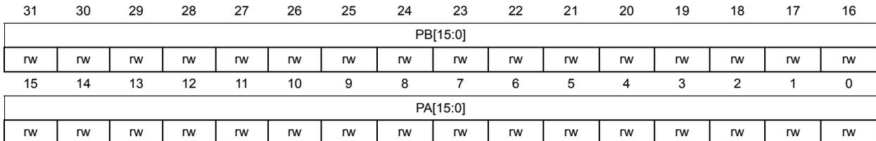
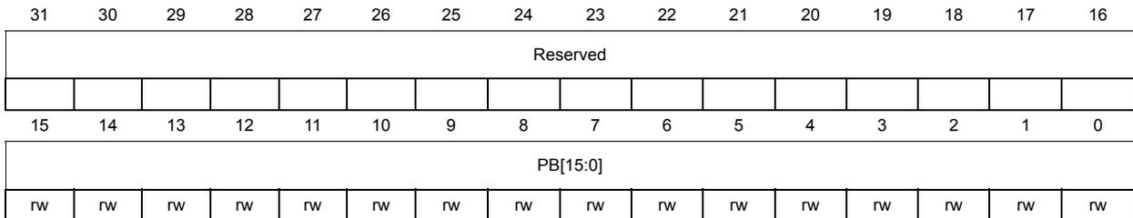
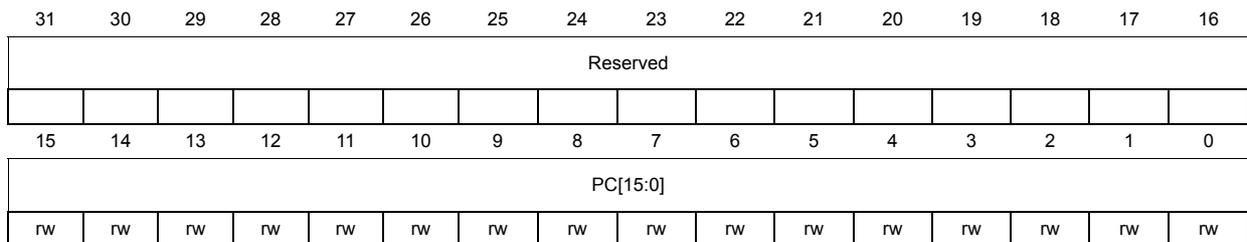
8.4.4 RI hysteresis control register (RI_HYSCR1)
The RI_HYSCR1 register is used to enable/disable the hysteresis of the input Schmitt trigger of ports A and B.
Address offset: 0x0C
Reset value: 0x0000 0000
| 31 | 30 | 29 | 28 | 27 | 26 | 25 | 24 | 23 | 22 | 21 | 20 | 19 | 18 | 17 | 16 |
| PB[15:0] | |||||||||||||||
| rw | rw | rw | rw | rw | rw | rw | rw | rw | rw | rw | rw | rw | rw | rw | rw |
| 15 | 14 | 13 | 12 | 11 | 10 | 9 | 8 | 7 | 6 | 5 | 4 | 3 | 2 | 1 | 0 |
| PA[15:0] | |||||||||||||||
| rw | rw | rw | rw | rw | rw | rw | rw | rw | rw | rw | rw | rw | rw | rw | rw |
Bits 31:16 PB[15:0] : Port B hysteresis control on/off
These bits are set and cleared by software to control the Schmitt trigger hysteresis of the Port B[15:0].
0: Hysteresis on
1: Hysteresis off
Bits 15:0 PA[15:0] : Port A hysteresis control on/off
These bits are set and cleared by software to control the Schmitt trigger hysteresis of the Port A[15:0].
0: Hysteresis on
1: Hysteresis off
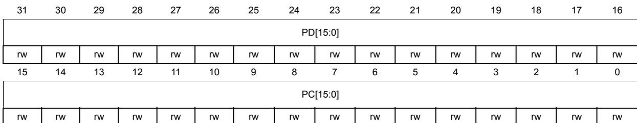
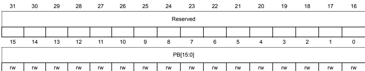
8.4.5 RI Hysteresis control register (RI_HYSCR2)
RI_HYSCR2 register enables/disables hysteresis of input Schmitt trigger of ports C and D.
Address offset: 0x10
Reset value: 0x0000 0000
| 31 | 30 | 29 | 28 | 27 | 26 | 25 | 24 | 23 | 22 | 21 | 20 | 19 | 18 | 17 | 16 |
| PD[15:0] | |||||||||||||||
| rw | rw | rw | rw | rw | rw | rw | rw | rw | rw | rw | rw | rw | rw | rw | rw |
| 15 | 14 | 13 | 12 | 11 | 10 | 9 | 8 | 7 | 6 | 5 | 4 | 3 | 2 | 1 | 0 |
| PC[15:0] | |||||||||||||||
| rw | rw | rw | rw | rw | rw | rw | rw | rw | rw | rw | rw | rw | rw | rw | rw |
Bits 31:16 PD[15:0] : Port D hysteresis control on/off
These bits are set and cleared by software to control the Schmitt trigger hysteresis of the Port D[15:0].
0: Hysteresis on
1: Hysteresis off
Bits 15:0 PC[15:0] : Port C hysteresis control on/off
These bits are set and cleared by software to control the Schmitt trigger hysteresis of the Port C[15:0].
0: Hysteresis on
1: Hysteresis off
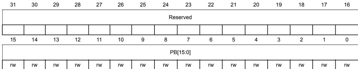
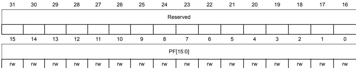
8.4.6 RI Hysteresis control register (RI_HYSCR3)
The RI_HYSCR3 register is used to enable/disable the hysteresis of the input Schmitt trigger of the entire port E and F.
Address offset: 0x14
Reset value: 0x0000 0000
| 31 | 30 | 29 | 28 | 27 | 26 | 25 | 24 | 23 | 22 | 21 | 20 | 19 | 18 | 17 | 16 |
|---|---|---|---|---|---|---|---|---|---|---|---|---|---|---|---|
| PF[15:0] | |||||||||||||||
| rw | rw | rw | rw | rw | rw | rw | rw | rw | rw | rw | rw | rw | rw | rw | rw |
| 15 | 14 | 13 | 12 | 11 | 10 | 9 | 8 | 7 | 6 | 5 | 4 | 3 | 2 | 1 | 0 |
| PE[15:0] | |||||||||||||||
| rw | rw | rw | rw | rw | rw | rw | rw | rw | rw | rw | rw | rw | rw | rw | rw |
Bits 31:16 PF[15:0] : Port F hysteresis control on/off
These bits are set and cleared by software to control the Schmitt trigger hysteresis of the Port F[15:0].
0: Hysteresis on
1: Hysteresis off
Note: These bits are available in Cat.3, Cat.4, Cat.5 and Cat.6 devices only.
Bits 15:0 PE[15:0] : Port E hysteresis control on/off
These bits are set and cleared by software to control the Schmitt trigger hysteresis of the Port E[15:0].
0: Hysteresis on
1: Hysteresis off
8.4.7 RI Hysteresis control register (RI_HYSCR4)
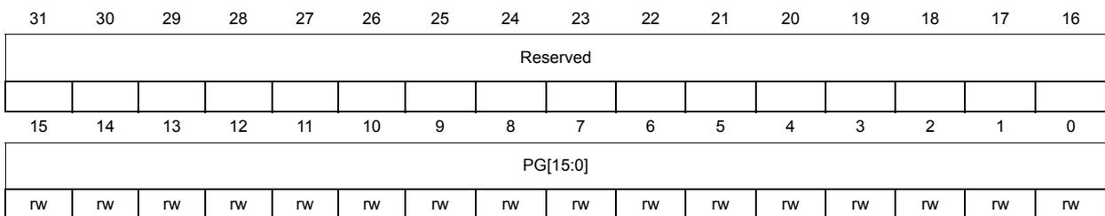
The RI_HYSCR4 register is used to enable/disable the hysteresis of the input Schmitt trigger of the entire port G.
Address offset: 0x18
Reset value: 0x0000 0000
| 31 | 30 | 29 | 28 | 27 | 26 | 25 | 24 | 23 | 22 | 21 | 20 | 19 | 18 | 17 | 16 |
|---|---|---|---|---|---|---|---|---|---|---|---|---|---|---|---|
| Reserved | |||||||||||||||
| 15 | 14 | 13 | 12 | 11 | 10 | 9 | 8 | 7 | 6 | 5 | 4 | 3 | 2 | 1 | 0 |
| PG[15:0] | |||||||||||||||
| rw | rw | rw | rw | rw | rw | rw | rw | rw | rw | rw | rw | rw | rw | rw | rw |
Bits 31:16 Reserved, must be kept at reset value
Bits 15:0 PG[15:0] : Port G hysteresis control on/off
These bits are set and cleared by software to control the Schmitt trigger hysteresis of the Port G[15:0].
0: Hysteresis on
1: Hysteresis off
Note: These bits are available in Cat.3, Cat.4, Cat.5 and Cat.6 devices only.
8.4.8 Analog switch mode register (RI_ASMR1)
The RI_ASMR1 register is available in Cat.3, Cat.4, Cat.5 and Cat.6 devices only and is used to select if analog switches of port A are to be controlled by the timer OC or through the ADC interface or RI_ASCRx registers.
Address offset: 0x1C
Reset value: 0x0000 0000
| 31 | 30 | 29 | 28 | 27 | 26 | 25 | 24 | 23 | 22 | 21 | 20 | 19 | 18 | 17 | 16 |
|---|---|---|---|---|---|---|---|---|---|---|---|---|---|---|---|
| Reserved | |||||||||||||||
| 15 | 14 | 13 | 12 | 11 | 10 | 9 | 8 | 7 | 6 | 5 | 4 | 3 | 2 | 1 | 0 |
| PA[15:0] | |||||||||||||||
| rw | rw | rw | rw | rw | rw | rw | rw | rw | rw | rw | rw | rw | rw | rw | rw |
Bits 31:16 Reserved, must be kept at reset value
Bits 15:0 PA[15:0] : Port A analog switch mode selection
These bits are set and cleared by software to select the mode of controlling the analog switches for Port A.
0: ADC interface or RI_ASCRx controlled
1: Timer controlled
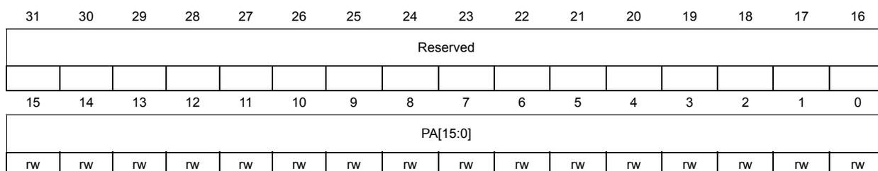
8.4.9 Channel mask register (RI_CMR1)
RI_CMR1 is available in Cat.3, Cat.4, Cat.5 and Cat.6 devices only and is used to mask a port A channel designated as a timer input capture (after acquisition completion to avoid triggering multiple detections).
Address offset: 0x20
Reset value: 0x0000 0000
| 31 | 30 | 29 | 28 | 27 | 26 | 25 | 24 | 23 | 22 | 21 | 20 | 19 | 18 | 17 | 16 |
| Reserved | |||||||||||||||
| 15 | 14 | 13 | 12 | 11 | 10 | 9 | 8 | 7 | 6 | 5 | 4 | 3 | 2 | 1 | 0 |
| PA[15:0] | |||||||||||||||
| rw | rw | rw | rw | rw | rw | rw | rw | rw | rw | rw | rw | rw | rw | rw | rw |
Bits 31:16 Reserved, must be kept at reset value
Bits 15:0 PA[15:0] : Port A channel masking
These bits are set and cleared by software to mask the input of port A during the capacitive sensing acquisition.
0: Masked
1: Not masked
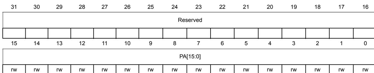
8.4.10 Channel identification for capture register (RI_CICR1)
The RI_CICR1 register is available in Cat.3, Cat.4, Cat.5 and Cat.6 devices only and is used when analog switches are controlled by a timer OC. RI_CICR1 allows a channel to be identified for timer input capture.
Address offset: 0x24
Reset value: 0x0000 0000
| 31 | 30 | 29 | 28 | 27 | 26 | 25 | 24 | 23 | 22 | 21 | 20 | 19 | 18 | 17 | 16 |
| Reserved | |||||||||||||||
| 15 | 14 | 13 | 12 | 11 | 10 | 9 | 8 | 7 | 6 | 5 | 4 | 3 | 2 | 1 | 0 |
| PA[15:0] | |||||||||||||||
| rw | rw | rw | rw | rw | rw | rw | rw | rw | rw | rw | rw | rw | rw | rw | rw |
Bits 31:16 Reserved, must be kept at reset value
Bits 15:0 PA[15:0] : Port A channel identification for capture
These bits are set and cleared by software to identify the sampling capacitor I/Os on Port A.
0: Channel I/O
1: Sampling capacitor I/O
8.4.11 Analog switch mode register (RI_ASMR2)
The RI_ASMR2 register is available in Cat.3, Cat.4, Cat.5 and Cat.6 devices only and is used to select if analog switches of port B are to be controlled by the timer OC or through the ADC interface or RI_ASCRx registers.
Address offset: 0x28
Reset value: 0x0000 0000
| 31 | 30 | 29 | 28 | 27 | 26 | 25 | 24 | 23 | 22 | 21 | 20 | 19 | 18 | 17 | 16 |
| Reserved | |||||||||||||||
| 15 | 14 | 13 | 12 | 11 | 10 | 9 | 8 | 7 | 6 | 5 | 4 | 3 | 2 | 1 | 0 |
| PB[15:0] | |||||||||||||||
| rw | rw | rw | rw | rw | rw | rw | rw | rw | rw | rw | rw | rw | rw | rw | rw |
Bits 31:16 Reserved, must be kept at reset value
Bits 15:0 PB[15:0] : Port B analog switch mode selection
These bits are set and cleared by software to select the mode of controlling the analog switches for Port B.
0: ADC interface or RI_ASCRx controlled
1: Timer controlled
8.4.12 Channel mask register (RI_CMR2)
RI_CMR2 is available in Cat.3, Cat.4, Cat.5 and Cat.6 devices only and is used to mask a port B channel designated as a timer input capture (after acquisition completion to avoid triggering multiple detections)
Address offset: 0x2C
Reset value: 0x0000 0000
| 31 | 30 | 29 | 28 | 27 | 26 | 25 | 24 | 23 | 22 | 21 | 20 | 19 | 18 | 17 | 16 |
| Reserved | |||||||||||||||
| 15 | 14 | 13 | 12 | 11 | 10 | 9 | 8 | 7 | 6 | 5 | 4 | 3 | 2 | 1 | 0 |
| PB[15:0] | |||||||||||||||
| rw | rw | rw | rw | rw | rw | rw | rw | rw | rw | rw | rw | rw | rw | rw | rw |
Bits 31:16 Reserved, must be kept at reset value
Bits 15:0 PB[15:0] : Port B channel masking
These bits are set and cleared by software to mask the input of port B during the capacitive sensing acquisition.
0: Masked
1: Not masked
8.4.13 Channel identification for capture register (RI_CICR2)
The RI_CICR2 register is available in Cat.3, Cat.4, Cat.5 and Cat.6 devices only and is used when analog switches are controlled by a timer OC. RI_CICR2 allows a port B channel to be identified for timer input capture.
Address offset: 0x30
Reset value: 0x0000 0000
| 31 | 30 | 29 | 28 | 27 | 26 | 25 | 24 | 23 | 22 | 21 | 20 | 19 | 18 | 17 | 16 |
| Reserved | |||||||||||||||
| 15 | 14 | 13 | 12 | 11 | 10 | 9 | 8 | 7 | 6 | 5 | 4 | 3 | 2 | 1 | 0 |
| PB[15:0] | |||||||||||||||
| rw | rw | rw | rw | rw | rw | rw | rw | rw | rw | rw | rw | rw | rw | rw | rw |
Bits 31:16 Reserved, must be kept at reset value
Bits 15:0 PB[15:0] : Port B channel identification for capture
These bits are set and cleared by software to identify the sampling capacitor I/Os on Port B.
0: Channel I/O
1: Sampling capacitor I/O
8.4.14 Analog switch mode register (RI_ASMR3)
The RI_ASMR3 register is available in Cat.3, Cat.4, Cat.5 and Cat.6 devices only and is used to select if analog switches of port C are to be controlled by the timer OC or through the ADC interface or RI_ASCRx registers.
Address offset: 0x34
Reset value: 0x0000 0000
| 31 | 30 | 29 | 28 | 27 | 26 | 25 | 24 | 23 | 22 | 21 | 20 | 19 | 18 | 17 | 16 |
| Reserved | |||||||||||||||
| 15 | 14 | 13 | 12 | 11 | 10 | 9 | 8 | 7 | 6 | 5 | 4 | 3 | 2 | 1 | 0 |
| PC[15:0] | |||||||||||||||
| rw | rw | rw | rw | rw | rw | rw | rw | rw | rw | rw | rw | rw | rw | rw | rw |
Bits 31:16 Reserved, must be kept at reset value
Bits 15:0 PC[15:0] : Port C analog switch mode selection
These bits are set and cleared by software to select the mode of controlling the analog switches for Port C.
0: ADC interface or RI_ASCRx controlled
1: Timer controlled
8.4.15 Channel mask register (RI_CMR3)
RI_CMR3 is available in Cat.3, Cat.4, Cat.5 and Cat.6 devices only and is used to mask a port C channel designated as a timer input capture (after acquisition completion to avoid triggering multiple detections)
Address offset: 0x38
Reset value: 0x0000 0000
| 31 | 30 | 29 | 28 | 27 | 26 | 25 | 24 | 23 | 22 | 21 | 20 | 19 | 18 | 17 | 16 |
| Reserved | |||||||||||||||
| 15 | 14 | 13 | 12 | 11 | 10 | 9 | 8 | 7 | 6 | 5 | 4 | 3 | 2 | 1 | 0 |
| PC[15:0] | |||||||||||||||
| rw | rw | rw | rw | rw | rw | rw | rw | rw | rw | rw | rw | rw | rw | rw | rw |
Bits 31:16 Reserved, must be kept at reset value
Bits 15:0 PC[15:0] : Port C channel masking
These bits are set and cleared by software to mask the input of port C during the capacitive sensing acquisition.
0: Masked
1: Not masked
8.4.16 Channel identification for capture register (RI_CICR3)
The RI_CICR3 register is available in Cat.3, Cat.4, Cat.5 and Cat.6 devices only and is used when analog switches are controlled by a timer OC. RI_CICR3 allows a port C channel to be identified for timer input capture.
Address offset: 0x3C
Reset value: 0x0000 0000
| 31 | 30 | 29 | 28 | 27 | 26 | 25 | 24 | 23 | 22 | 21 | 20 | 19 | 18 | 17 | 16 |
| Reserved | |||||||||||||||
| 15 | 14 | 13 | 12 | 11 | 10 | 9 | 8 | 7 | 6 | 5 | 4 | 3 | 2 | 1 | 0 |
| PC[15:0] | |||||||||||||||
| rw | rw | rw | rw | rw | rw | rw | rw | rw | rw | rw | rw | rw | rw | rw | rw |
Bits 31:16 Reserved, must be kept at reset value
Bits 15:0 PC[15:0] : Port C channel identification for capture
These bits are set and cleared by software to identify the sampling capacitor I/Os on Port C.
0: Channel I/O
1: Sampling capacitor I/O
8.4.17 Analog switch mode register (RI_ASMR4)
The RI_ASMR4 register is available in Cat.3, Cat.4, Cat.5 and Cat.6 devices only and is used to select if analog switches of port F are to be controlled by the timer OC or through the ADC interface or RI_ASCRx registers.
Address offset: 0x40
Reset value: 0x0000 0000
| 31 | 30 | 29 | 28 | 27 | 26 | 25 | 24 | 23 | 22 | 21 | 20 | 19 | 18 | 17 | 16 |
| Reserved | |||||||||||||||
| 15 | 14 | 13 | 12 | 11 | 10 | 9 | 8 | 7 | 6 | 5 | 4 | 3 | 2 | 1 | 0 |
| PF[15:0] | |||||||||||||||
| rw | rw | rw | rw | rw | rw | rw | rw | rw | rw | rw | rw | rw | rw | rw | rw |
Bits 31:16 Reserved, must be kept at reset value
Bits 15:0 PF[15:0]: Port F analog switch mode selection
These bits are set and cleared by software to select the mode of controlling the analog switches for Port F.
0: ADC interface or RI_ASCRx controlled
1: Timer controlled
Note: These bits are available in Cat.3, Cat.4, Cat.5 and Cat.6 devices only.
8.4.18 Channel mask register (RI_CMR4)
RI_CMR4 is available in Cat.3, Cat.4, Cat.5 and Cat.6 devices only and is used to mask a port F channel designated as a timer input capture (after acquisition completion to avoid triggering multiple detections).
Address offset: 0x44
Reset value: 0x0000 0000
| 31 | 30 | 29 | 28 | 27 | 26 | 25 | 24 | 23 | 22 | 21 | 20 | 19 | 18 | 17 | 16 |
| Reserved | |||||||||||||||
| 15 | 14 | 13 | 12 | 11 | 10 | 9 | 8 | 7 | 6 | 5 | 4 | 3 | 2 | 1 | 0 |
| PF[15:0] | |||||||||||||||
| rw | rw | rw | rw | rw | rw | rw | rw | rw | rw | rw | rw | rw | rw | rw | rw |
Bits 31:16 Reserved, must be kept at reset value
Bits 15:0 PF[15:0]: Port F channel masking
These bits are set and cleared by software to mask the input of port F during the capacitive sensing acquisition.
0: Masked
1: Not masked
Note: These bits are available in Cat.3, Cat.4, Cat.5 and Cat.6 devices only.
8.4.19 Channel identification for capture register (RI_CICR4)
The RI_CICR4 register is available in Cat.3, Cat.4, Cat.5 and Cat.6 devices only and is used when analog switches are controlled by a timer OC. RI_CICR4 allows a port F channel to be identified for timer input capture.
Address offset: 0x48
Reset value: 0x0000 0000
| 31 | 30 | 29 | 28 | 27 | 26 | 25 | 24 | 23 | 22 | 21 | 20 | 19 | 18 | 17 | 16 |
| Reserved | |||||||||||||||
| 15 | 14 | 13 | 12 | 11 | 10 | 9 | 8 | 7 | 6 | 5 | 4 | 3 | 2 | 1 | 0 |
| PF[15:0] | |||||||||||||||
| rw | rw | rw | rw | rw | rw | rw | rw | rw | rw | rw | rw | rw | rw | rw | rw |
Bits 31:16 Reserved, must be kept at reset value
Bits 15:0 PF[15:0] : Port F channel identification for capture
These bits are set and cleared by software to identify the sampling capacitor I/Os on Port F.
0: Channel I/O
1: Sampling capacitor I/O
Note: These bits are available in Cat.3, Cat.4, Cat.5 and Cat.6 devices only.
8.4.20 Analog switch mode register (RI_ASMR5)
The RI_ASMR5 register is available in Cat.3, Cat.4, Cat.5 and Cat.6 devices only and is used to select if analog switches of port G are to be controlled by the timer OC or through the ADC interface or RI_ASCRx registers.
Address offset: 0x4C
Reset value: 0x0000 0000
| 31 | 30 | 29 | 28 | 27 | 26 | 25 | 24 | 23 | 22 | 21 | 20 | 19 | 18 | 17 | 16 |
| Reserved | |||||||||||||||
| 15 | 14 | 13 | 12 | 11 | 10 | 9 | 8 | 7 | 6 | 5 | 4 | 3 | 2 | 1 | 0 |
| PG[15:0] | |||||||||||||||
| rw | rw | rw | rw | rw | rw | rw | rw | rw | rw | rw | rw | rw | rw | rw | rw |
Bits 31:16 Reserved, must be kept at reset value
Bits 15:0 PG[15:0] : Port G analog switch mode selection
These bits are set and cleared by software to select the mode of controlling the analog switches for Port G.
0: ADC interface or RI_ASCRx controlled
1: Timer controlled
Note: These bits are available in Cat.3, Cat.4, Cat.5 and Cat.6 devices only.
8.4.21 Channel mask register (RI_CMR5)
RI_CMR5 is available in Cat.3, Cat.4, Cat.5 and Cat.6 devices only and is used to mask a port G channel designated as a timer input capture (after acquisition completion to avoid triggering multiple detections).
Address offset: 0x50
Reset value: 0x0000 0000
| 31 | 30 | 29 | 28 | 27 | 26 | 25 | 24 | 23 | 22 | 21 | 20 | 19 | 18 | 17 | 16 |
| Reserved | |||||||||||||||
| 15 | 14 | 13 | 12 | 11 | 10 | 9 | 8 | 7 | 6 | 5 | 4 | 3 | 2 | 1 | 0 |
| PG[15:0] | |||||||||||||||
| rw | rw | rw | rw | rw | rw | rw | rw | rw | rw | rw | rw | rw | rw | rw | rw |
Bits 31:16 Reserved, must be kept at reset value
Bits 15:0 PG[15:0]: Port G channel masking
These bits are set and cleared by software to mask the input of port G during the capacitive sensing acquisition.
0: Masked
1: Not masked
Note: These bits are available in Cat.3, Cat.4, Cat.5 and Cat.6 devices only.
8.4.22 Channel identification for capture register (RI_CICR5)
The RI_CICR5 register is available in Cat.3, Cat.4, Cat.5 and Cat.6 devices only and is used when analog switches are controlled by a timer OC. RI_CICR5 allows a port G channel to be identified for timer input capture.
Address offset: 0x54
Reset value: 0x0000 0000

| 31 | 30 | 29 | 28 | 27 | 26 | 25 | 24 | 23 | 22 | 21 | 20 | 19 | 18 | 17 | 16 |
| Reserved | |||||||||||||||
| 15 | 14 | 13 | 12 | 11 | 10 | 9 | 8 | 7 | 6 | 5 | 4 | 3 | 2 | 1 | 0 |
| PG[15:0] | |||||||||||||||
| rw | rw | rw | rw | rw | rw | rw | rw | rw | rw | rw | rw | rw | rw | rw | rw |
Bits 31:16 Reserved, must be kept at reset value
Bits 15:0 PG[15:0]: Port G channel identification for capture
These bits are set and cleared by software to identify the sampling capacitor I/Os on Port G.
0: Channel I/O
1: Sampling capacitor I/O
Note: These bits are available in Cat.3, Cat.4, Cat.5 and Cat.6 devices only.
8.4.23 RI register map
Table 45 summarizes the RI registers. The reserved memory areas are highlighted in gray in the table.
Table 45. RI register map and reset values
| Offset | Register | 31 | 30 | 29 | 28 | 27 | 26 | 25 | 24 | 23 | 22 | 21 | 20 | 19 | 18 | 17 | 16 | 15 | 14 | 13 | 12 | 11 | 10 | 9 | 8 | 7 | 6 | 5 | 4 | 3 | 2 | 1 | 0 |
|---|---|---|---|---|---|---|---|---|---|---|---|---|---|---|---|---|---|---|---|---|---|---|---|---|---|---|---|---|---|---|---|---|---|
| 0x00 | RI_ICR | Reserved | IC 4 | IC 3 | IC 2 | IC 1 | TIM[1:0] | IC4IOS[3:0] | IC3IOS[3:0] | IC2IOS[3:0] | IC1IOS[3:0] | ||||||||||||||||||||||
| Reset value | 0 | 0 | 0 | 0 | 0 | 0 | 0 | 0 | 0 | 0 | 0 | 0 | 0 | 0 | 0 | 0 | 0 | 0 | 0 | 0 | 0 | 0 | |||||||||||
| 0x04 | RI_ASCR 1 | SCM | GR11[4:1] | VCOMP | CH25:22 | GR7[4:1] | Reserved | GR11:5 | GR9 [2:1] | GR8[4:1] | GR3 [2:1] | GR2 [2:1] | CH5 | CH4 | GR1[4:1] | ||||||||||||||||||
| Reset value | 0 | 0 | 0 | 0 | 0 | 0 | 0 | 0 | 0 | 0 | 0 | 0 | 0 | 0 | 0 | 0 | 0 | 0 | 0 | 0 | 0 | 0 | 0 | 0 | 0 | 0 | 0 | 0 | 0 | 0 | 0 | ||
| 0x08 | RI_ASCR 2 | Reserved | GR6 [4:3] | GR7[7:5] | GR2[5:3] | GR9 [4:3] | GR3[5:3] | Reserved | GR4[3:1] | GR5[3:1] | GR6 [2:1] | GR10[4:1] | |||||||||||||||||||||
| Reset value | 0 | 0 | 0 | 0 | 0 | 0 | 0 | 0 | 0 | 0 | 0 | 0 | 0 | 0 | 0 | 0 | 0 | 0 | 0 | 0 | 0 | 0 | 0 | 0 | |||||||||
| 0x0C | RI_HYSC R1 | PB[15:0] | |||||||||||||||||||||||||||||||
| Reset value | 0 | 0 | 0 | 0 | 0 | 0 | 0 | 0 | 0 | 0 | 0 | 0 | 0 | 0 | 0 | 0 | 0 | 0 | 0 | 0 | 0 | 0 | 0 | 0 | 0 | 0 | 0 | 0 | 0 | 0 | 0 | 0 | |
| 0x10 | RI_HYSC R2 | PD[15:0] | |||||||||||||||||||||||||||||||
| Reset value | 0 | 0 | 0 | 0 | 0 | 0 | 0 | 0 | 0 | 0 | 0 | 0 | 0 | 0 | 0 | 0 | 0 | 0 | 0 | 0 | 0 | 0 | 0 | 0 | 0 | 0 | 0 | 0 | 0 | 0 | 0 | 0 | |
| 0x14 | RI_HYSC R3 | PF[15:0] | |||||||||||||||||||||||||||||||
| Reset value | 0 | 0 | 0 | 0 | 0 | 0 | 0 | 0 | 0 | 0 | 0 | 0 | 0 | 0 | 0 | 0 | 0 | 0 | 0 | 0 | 0 | 0 | 0 | 0 | 0 | 0 | 0 | 0 | 0 | 0 | 0 | 0 | |
| 0x18 | RI_HYSC R4 | Reserved | |||||||||||||||||||||||||||||||
| Reset value | |||||||||||||||||||||||||||||||||
| 0x1C | RI_ASMR 1 | Reserved | |||||||||||||||||||||||||||||||
| Reset value | |||||||||||||||||||||||||||||||||
| 0x20 | RI_CMR1 | Reserved | |||||||||||||||||||||||||||||||
| Reset value | |||||||||||||||||||||||||||||||||
| 0x24 | RI_CICR1 | Reserved | |||||||||||||||||||||||||||||||
| Reset value | |||||||||||||||||||||||||||||||||
| 0x28 | RI_ASMR 2 | Reserved | |||||||||||||||||||||||||||||||
| Reset value | |||||||||||||||||||||||||||||||||
Table 45. RI register map and reset values (continued)
| Offset | Register | 31 | 30 | 29 | 28 | 27 | 26 | 25 | 24 | 23 | 22 | 21 | 20 | 19 | 18 | 17 | 16 | 15 | 14 | 13 | 12 | 11 | 10 | 9 | 8 | 7 | 6 | 5 | 4 | 3 | 2 | 1 | 0 |
|---|---|---|---|---|---|---|---|---|---|---|---|---|---|---|---|---|---|---|---|---|---|---|---|---|---|---|---|---|---|---|---|---|---|
| 0x2C | RI_CMR2 | Reserved | PB[15:0] | ||||||||||||||||||||||||||||||
| Reset value | 0 | 0 | 0 | 0 | 0 | 0 | 0 | 0 | 0 | 0 | 0 | 0 | 0 | 0 | 0 | 0 | |||||||||||||||||
| 0x30 | RI_CICR2 | Reserved | PB[15:0] | ||||||||||||||||||||||||||||||
| Reset value | 0 | 0 | 0 | 0 | 0 | 0 | 0 | 0 | 0 | 0 | 0 | 0 | 0 | 0 | 0 | 0 | |||||||||||||||||
| 0x34 | RI_ASMR3 | Reserved | PC[15:0] | ||||||||||||||||||||||||||||||
| Reset value | 0 | 0 | 0 | 0 | 0 | 0 | 0 | 0 | 0 | 0 | 0 | 0 | 0 | 0 | 0 | 0 | |||||||||||||||||
| 0x38 | RI_CMR3 | Reserved | PC[15:0] | ||||||||||||||||||||||||||||||
| Reset value | 0 | 0 | 0 | 0 | 0 | 0 | 0 | 0 | 0 | 0 | 0 | 0 | 0 | 0 | 0 | 0 | |||||||||||||||||
| 0x3C | RI_CICR3 | Reserved | PC[15:0] | ||||||||||||||||||||||||||||||
| Reset value | 0 | 0 | 0 | 0 | 0 | 0 | 0 | 0 | 0 | 0 | 0 | 0 | 0 | 0 | 0 | 0 | |||||||||||||||||
| 0x40 | RI_ASMR4 | Reserved | PF[15:0] | ||||||||||||||||||||||||||||||
| Reset value | 0 | 0 | 0 | 0 | 0 | 0 | 0 | 0 | 0 | 0 | 0 | 0 | 0 | 0 | 0 | 0 | |||||||||||||||||
| 0x44 | RI_CMR4 | Reserved | PF[15:0] | ||||||||||||||||||||||||||||||
| Reset value | 0 | 0 | 0 | 0 | 0 | 0 | 0 | 0 | 0 | 0 | 0 | 0 | 0 | 0 | 0 | 0 | |||||||||||||||||
| 0x48 | RI_CICR4 | Reserved | PF[15:0] | ||||||||||||||||||||||||||||||
| Reset value | 0 | 0 | 0 | 0 | 0 | 0 | 0 | 0 | 0 | 0 | 0 | 0 | 0 | 0 | 0 | 0 | |||||||||||||||||
| 0x4C | RI_ASMR5 | Reserved | PG[15:0] | ||||||||||||||||||||||||||||||
| Reset value | 0 | 0 | 0 | 0 | 0 | 0 | 0 | 0 | 0 | 0 | 0 | 0 | 0 | 0 | 0 | 0 | |||||||||||||||||
| 0x50 | RI_CMR5 | Reserved | PG[15:0] | ||||||||||||||||||||||||||||||
| Reset value | 0 | 0 | 0 | 0 | 0 | 0 | 0 | 0 | 0 | 0 | 0 | 0 | 0 | 0 | 0 | 0 | |||||||||||||||||
| 0x54 | RI_CICR5 | Reserved | PG[15:0] | ||||||||||||||||||||||||||||||
| Reset value | 0 | 0 | 0 | 0 | 0 | 0 | 0 | 0 | 0 | 0 | 0 | 0 | 0 | 0 | 0 | 0 | |||||||||||||||||
8.5 SYSCFG registers
The peripheral registers have to be accessed by words (32-bit).
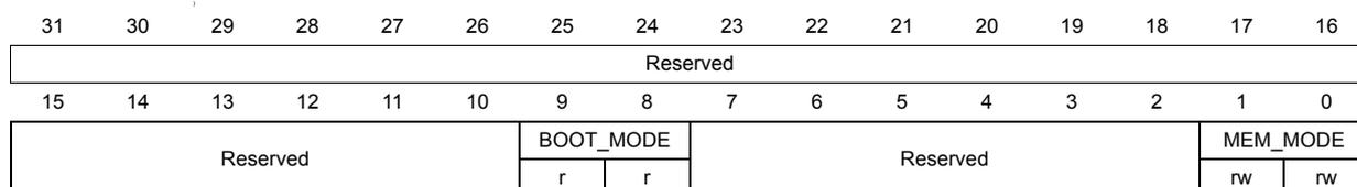
8.5.1 SYSCFG memory remap register (SYSCFG_MEMRMP)
This register is used for specific configurations on memory remap:
- • Two bits are used to configure the type of memory accessible at address 0x0000 0000. These bits are used to select the physical remap by software and so, bypass the BOOT pins.
- • After reset these bits take the value selected by the BOOT pins.
Note: This register is not reset through the SYSCFGRST bit in the RCC_APB2RSTR register.
Address offset: 0x00
Reset value: 0x0000 00XX (X is the memory mode selected by the BOOT pins)
| 31 | 30 | 29 | 28 | 27 | 26 | 25 | 24 | 23 | 22 | 21 | 20 | 19 | 18 | 17 | 16 |
| Reserved | |||||||||||||||
| 15 | 14 | 13 | 12 | 11 | 10 | 9 | 8 | 7 | 6 | 5 | 4 | 3 | 2 | 1 | 0 |
| Reserved | BOOT_MODE | Reserved | MEM_MODE | ||||||||||||
| r | r | nw | nw | ||||||||||||
Bits 31:10 Reserved
Bits 9:8 BOOT_MODE : Boot mode selected by the boot pins
These bits are read only. They indicate the boot mode selected by the boot pins. Bit 9 corresponds to the value sampled on the BOOT1 pin, and bit 8 corresponds to value sampled on the BOOT0 pin. See also Section 2.7: Boot configuration on page 50 .
- 00: Main Flash memory boot mode
- 01: System Flash memory boot mode
- 10: Reserved
- 11: Embedded SRAM boot mode
Bits 7:2 Reserved
Bits 1:0 MEM_MODE : Memory mapping selection
Set and cleared by software. This bit controls the memory's internal mapping at address 0x0000 0000. After reset these bits take on the memory mapping selected by the BOOT pins.
- 00: Main Flash memory mapped at 0x0000 0000
- 01: System Flash memory mapped at 0x0000 0000
- 10: FSMC
- 11: SRAM mapped at 0x0000 0000
8.5.2 SYSCFG peripheral mode configuration register (SYSCFG_PMC)
An internal pull-up resistor (1.5 k \( \Omega \) ) can be connected by software on the USB data + (DP) line. This internal pull-up resistor is enabled if the USB is not in power-down mode and if the USB_PU bit is set.
Address offset: 0x04
Reset value: 0x0000 0000
| 31 | 30 | 29 | 28 | 27 | 26 | 25 | 24 | 23 | 22 | 21 | 20 | 19 | 18 | 17 | 16 |
| Reserved | |||||||||||||||
| 15 | 14 | 13 | 12 | 11 | 10 | 9 | 8 | 7 | 6 | 5 | 4 | 3 | 2 | 1 | 0 |
| Reserved | LCD_CAPA | USB_PU | |||||||||||||
| rw | rw | ||||||||||||||
Bits 31:6 Reserved
Bit 5:1
LCD_CAPA
decoupling capacitance connection
(see device datasheet for this device capability)
Bit 1 controls the connection of
\(
V_{LCDrail2}
\)
on PB2/LCD_VCAP2
0:
\(
V_{LCDrail2}
\)
not connected to PB2/LCD_VCAP2
1:
\(
V_{LCDrail2}
\)
connected to PB2/LCD_VCAP2
Bit 2 controls the connection of
\(
V_{LCDrail1}
\)
on PB12/LCD_VCAP1
Bit 3 controls the connection of
\(
V_{LCDrail3}
\)
on PB0/LCD_VCAP3
Bit 4 controls the connection of
\(
V_{LCDrail1}
\)
on PE11/LCD_VCAP1
Bit 5 controls the connection of
\(
V_{LCDrail3}
\)
on PE12/LCD_VCAP3
Bit 0 USB_PU USB pull-up enable on DP line
Set and cleared by software. This bit controls the internal pull-up (1.5 k
\(
\Omega
\)
) on the USB DP line.
0: no pull-up on the USB DP line (even if USB is not in power down mode)
1: internal pull-up is connected on USB DP line (only if USB is not in power down mode)
8.5.3 SYSCFG external interrupt configuration register 1 (SYSCFG_EXTICR1)
Address offset: 0x08
Reset value: 0x0000
| 31 | 30 | 29 | 28 | 27 | 26 | 25 | 24 | 23 | 22 | 21 | 20 | 19 | 18 | 17 | 16 |
| Reserved | |||||||||||||||
| 15 | 14 | 13 | 12 | 11 | 10 | 9 | 8 | 7 | 6 | 5 | 4 | 3 | 2 | 1 | 0 |
| EXTI3[3:0] | EXTI2[3:0] | EXTI1[3:0] | EXTI0[3:0] | ||||||||||||
| rw | rw | rw | rw | rw | rw | rw | rw | rw | rw | rw | rw | rw | rw | rw | rw |
Bits 31:16 Reserved
Bits 15:0 EXTIx[3:0] : EXTI x configuration (x = 0 to 3)
These bits are written by software to select the source input for the EXTEx external interrupt.
0000: PA[x] pin
0001: PB[x] pin
0010: PC[x] pin
0011: PD[x] pin
0100: PE[x] pin
0101: PH[x] (only PH[2:0], PH3 is not available)
0110: PF[x] pin (Cat.3, Cat.4, Cat.5 and Cat.6 devices only)
0111: PG[x] pin (Cat.3, Cat.4, Cat.5 and Cat.6 devices only)
8.5.4 SYSCFG external interrupt configuration register 2 (SYSCFG_EXTICR2)
Address offset: 0x0C
Reset value: 0x0000
| 31 | 30 | 29 | 28 | 27 | 26 | 25 | 24 | 23 | 22 | 21 | 20 | 19 | 18 | 17 | 16 |
|---|---|---|---|---|---|---|---|---|---|---|---|---|---|---|---|
| Reserved | |||||||||||||||
| 15 | 14 | 13 | 12 | 11 | 10 | 9 | 8 | 7 | 6 | 5 | 4 | 3 | 2 | 1 | 0 |
| EXTI7[3:0] | EXTI6[3:0] | EXTI5[3:0] | EXTI4[3:0] | ||||||||||||
| rw | rw | rw | rw | rw | rw | rw | rw | rw | rw | rw | rw | rw | rw | rw | rw |
Bits 31:16 Reserved
Bits 15:0 EXTIx[3:0] : EXTI x configuration (x = 4 to 7)
These bits are written by software to select the source input for the EXTIx external interrupt.
0000: PA[x] pin
0001: PB[x] pin
0010: PC[x] pin
0011: PD[x] pin
0100: PE[x] pin
0110: PF[x] pin (Cat.3, Cat.4, Cat.5 and Cat.6 devices only)
0111: PG[x] pin (Cat.3, Cat.4, Cat.5 and Cat.6 devices only)
PH[7:4] are not available.
8.5.5 SYSCFG external interrupt configuration register 3 (SYSCFG_EXTICR3)
Address offset: 0x10
Reset value: 0x0000
| 31 | 30 | 29 | 28 | 27 | 26 | 25 | 24 | 23 | 22 | 21 | 20 | 19 | 18 | 17 | 16 |
|---|---|---|---|---|---|---|---|---|---|---|---|---|---|---|---|
| Reserved | |||||||||||||||
| 15 | 14 | 13 | 12 | 11 | 10 | 9 | 8 | 7 | 6 | 5 | 4 | 3 | 2 | 1 | 0 |
| EXTI11[3:0] | EXTI10[3:0] | EXTI9[3:0] | EXTI8[3:0] | ||||||||||||
| rw | rw | rw | rw | rw | rw | rw | rw | rw | rw | rw | rw | rw | rw | rw | rw |
Bits 31:16 Reserved
Bits 15:0 EXTIx[3:0] : EXTI x configuration (x = 8 to 11)
These bits are written by software to select the source input for the EXTIx external interrupt.
0000: PA[x] pin
0001: PB[x] pin
0010: PC[x] pin
0011: PD[x] pin
0100: PE[x] pin
0110: PF[x] pin (Cat.3, Cat.4, Cat.5 and Cat.6 devices only)
0111: PG[x] pin (Cat.3, Cat.4, Cat.5 and Cat.6 devices only)
PH[11:8] are not available.
8.5.6 SYSCFG external interrupt configuration register 4 (SYSCFG_EXTICR4)
Address offset: 0x14
Reset value: 0x0000
| 31 | 30 | 29 | 28 | 27 | 26 | 25 | 24 | 23 | 22 | 21 | 20 | 19 | 18 | 17 | 16 |
|---|---|---|---|---|---|---|---|---|---|---|---|---|---|---|---|
| Reserved | |||||||||||||||
| 15 | 14 | 13 | 12 | 11 | 10 | 9 | 8 | 7 | 6 | 5 | 4 | 3 | 2 | 1 | 0 |
| EXTI15[3:0] | EXTI14[3:0] | EXTI13[3:0] | EXTI12[3:0] | ||||||||||||
| rw | rw | rw | rw | rw | rw | rw | rw | rw | rw | rw | rw | rw | rw | rw | rw |
Bits 31:16 Reserved
Bits 15:0 EXTIx[3:0] : EXTI x configuration (x = 12 to 15)
These bits are written by software to select the source input for the EXTIx external interrupt.
0000: PA[x] pin
0001: PB[x] pin
0010: PC[x] pin
0011: PD[x] pin
0100: PE[x] pin
0110: PF[x] pin (Cat.3, Cat.4, Cat.5 and Cat.6 devices only)
0111: PG[x] pin (Cat.3, Cat.4, Cat.5 and Cat.6 devices only)
PH[15:12] are not available.
8.5.7 SYSCFG register map
The following table gives the SYSCFG register map and the reset values. The reserved memory areas are highlighted in gray in the table.
Table 46. SYSCFG register map and reset values
| Offset | Register | 31 | 30 | 29 | 28 | 27 | 26 | 25 | 24 | 23 | 22 | 21 | 20 | 19 | 18 | 17 | 16 | 15 | 14 | 13 | 12 | 11 | 10 | 9 | 8 | 7 | 6 | 5 | 4 | 3 | 2 | 1 | 0 |
|---|---|---|---|---|---|---|---|---|---|---|---|---|---|---|---|---|---|---|---|---|---|---|---|---|---|---|---|---|---|---|---|---|---|
| 0x00 | SYSCFG_MEMRMP | Reserved | |||||||||||||||||||||||||||||||
| Reset value | |||||||||||||||||||||||||||||||||
| 0x04 | SYSCFG_PMC | Reserved | |||||||||||||||||||||||||||||||
| Reset value | |||||||||||||||||||||||||||||||||
Table 46. SYSCFG register map and reset values (continued)
| Offset | Register | 31 | 30 | 29 | 28 | 27 | 26 | 25 | 24 | 23 | 22 | 21 | 20 | 19 | 18 | 17 | 16 | 15 | 14 | 13 | 12 | 11 | 10 | 9 | 8 | 7 | 6 | 5 | 4 | 3 | 2 | 1 | 0 |
|---|---|---|---|---|---|---|---|---|---|---|---|---|---|---|---|---|---|---|---|---|---|---|---|---|---|---|---|---|---|---|---|---|---|
| 0x08 | SYSCFG_EXTICR1 | Reserved | EXTI3[3:0] | EXTI2[3:0] | EXTI1[3:0] | EXTI0[3:0] | |||||||||||||||||||||||||||
| Reset value | 0 0 0 0 | 0 0 0 0 | 0 0 0 0 | 0 0 0 0 | |||||||||||||||||||||||||||||
| 0x0C | SYSCFG_EXTICR2 | Reserved | EXTI7[3:0] | EXTI6[3:0] | EXTI5[3:0] | EXTI4[3:0] | |||||||||||||||||||||||||||
| Reset value | 0 0 0 0 | 0 0 0 0 | 0 0 0 0 | 0 0 0 0 | |||||||||||||||||||||||||||||
| 0x10 | SYSCFG_EXTICR3 | Reserved | EXTI11[3:0] | EXTI10[3:0] | EXTI9[3:0] | EXTI8[3:0] | |||||||||||||||||||||||||||
| Reset value | 0 0 0 0 | 0 0 0 0 | 0 0 0 0 | 0 0 0 0 | |||||||||||||||||||||||||||||
| 0x14 | SYSCFG_EXTICR4 | Reserved | EXTI15[3:0] | EXTI14[3:0] | EXTI13[3:0] | EXTI12[3:0] | |||||||||||||||||||||||||||
| Reset value | 0 0 0 0 | 0 0 0 0 | 0 0 0 0 | 0 0 0 0 | |||||||||||||||||||||||||||||