6. Reset and clock control (RCC)
6.1 Reset
There are three types of reset, defined as system reset, power reset and RTC domain reset.
6.1.1 System reset
A system reset sets all registers to their reset values unless otherwise specified in the register description.
A system reset is generated when one of the following events occurs:
- 1. A low level on the NRST pin (external reset)
- 2. Window watchdog end-of-count condition (WWDG reset)
- 3. Independent watchdog end-of-count condition (IWDG reset)
- 4. A software reset (SW reset) (see Software reset )
- 5. Low-power management reset (see Low-power management reset )
- 6. Option byte loader reset (see Option byte loader reset )
- 7. Exit from Standby mode
The reset source can be identified by checking the reset flags in the control/status register, RCC_CSR (see Section 6.3.14 ).
Software reset
The SYSRESETREQ bit in Cortex ® -M3 Application Interrupt and Reset Control Register must be set to force a software reset on the device. Refer to the Cortex ® -M3 technical reference manual for more details.
Low-power management reset
There are two ways to generate a low-power management reset:
- 1. Reset generated when entering Standby mode:
This type of reset is enabled by resetting nRST_STDBY bit in user option bytes. In this case, whenever a Standby mode entry sequence is successfully executed, the device is reset instead of entering Standby mode. - 2. Reset when entering Stop mode:
This type of reset is enabled by resetting nRST_STOP bit in user option bytes. In this case, whenever a Stop mode entry sequence is successfully executed, the device is reset instead of entering Stop mode.
Option byte loader reset
The Option byte loader reset is generated when the OBL_LAUNCH bit (bit 18) is set in the FLASH_PECR register. This bit is used to launch by software the option byte loading.
For further information on the user option bytes, refer to Section 3: Flash program memory and data EEPROM (FLASH) .
6.1.2 Power reset
A power reset is generated when one of the following events occurs:
- 1. Power-on/power-down reset (POR/PDR reset)
- 2. BOR reset
A power reset sets all registers to their reset values including for the RTC domain (see Figure 14 )
These sources act on the NRST pin and it is always kept low during the delay phase. The RESET service routine vector is fixed at address 0x0000_0004 in the memory map. For more details, refer to Table 49: Vector table (Cat.1 and Cat.2 devices) , Table 50: Vector table (Cat.3 devices) and Table 51: Vector table (Cat.4, Cat.5 and Cat.6 devices) .
The system reset signal provided to the device is output on the NRST pin. The pulse generator guarantees a minimum reset pulse duration of 20 µs for each internal reset source. In case of an external reset, the reset pulse is generated while the NRST pin is asserted low.
Figure 14. Simplified diagram of the reset circuit
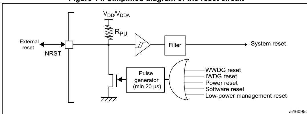
The diagram illustrates the internal reset circuitry. On the left, an 'External reset' signal is connected to the 'NRST' pin. The NRST pin is connected to a pull-up resistor \( R_{PU} \) tied to \( V_{DD}/V_{DDA} \) and a switch to ground. The NRST signal is also connected to a Schmitt trigger. The output of the Schmitt trigger is connected to a 'Filter' block, which outputs the 'System reset' signal. Below the Schmitt trigger, a 'Pulse generator (min 20 µs)' is connected to the NRST line via a transistor. The input of the pulse generator is connected to an OR gate. The OR gate receives inputs from 'WWDG reset', 'IWDG reset', 'Power reset', 'Software reset', and 'Low-power management reset'. The output of the filter is the 'System reset' signal. The diagram is labeled 'ai16095c' in the bottom right corner.
6.1.3 RTC and backup registers reset
The RTC peripheral, RTC clock source selection (in RCC_CSR) and the backup registers are reset only when one of the following events occurs:
- 1. A software reset, triggered by setting the RTCRST bit in the RCC_CSR register (see Section 6.3.14 )
- 2. Power reset (BOR/POR/PDR)
6.2 Clocks
Four different clock sources can be used to drive the system clock (SYSCLK):
- • HSI ((high-speed internal) oscillator clock
- • HSE (high-speed external) oscillator clock
- • PLL clock
- • MSI (multispeed internal) oscillator clock
The MSI is used as system clock source after startup from Reset, wake-up from Stop or Standby low-power modes.
The devices have the following two secondary clock sources:
- • 37 kHz low speed internal RC (LSI RC) which drives the independent watchdog and optionally the RTC used for Auto-wakeup from Stop/Standby mode.
- • 32.768 kHz low speed external crystal (LSE crystal) which optionally drives the real-time clock (RTCCLK)
Each clock source can be switched on or off independently when it is not used, to optimize power consumption.
Several prescalers allow the configuration of the AHB frequency, the high speed APB (APB2) and the low speed APB (APB1) domains. The maximum frequency of the AHB, APB1 and the APB2 domains is 32 MHz. It may depend on the device voltage range, for more details, refer to the Dynamic voltage scaling management section in the PWR chapter.
All the peripheral clocks are derived from the system clock (SYSCLK) except:
- • The 48 MHz clock USB and SDIO clocks which are derived from the PLL VCO clock.
- • The ADC clock which is always the HSI clock. A divider by 1, 2 or 4 can be used to adapt the clock frequency to the device operating conditions. For more details refer to the Operating Power Supply Range section in the PWR chapter.
- • The RTC/LCD clock which is derived from the LSE, LSI or 1 MHz HSE_RTC (HSE divided by a programmable prescaler).
- • IWDG clock which is always the LSI clock.
The system clock (SYSCLK) frequency must be higher or equal to the RTC/LCD clock frequency.
The RCC feeds the Cortex ® System Timer (SysTick) external clock with the AHB clock (HCLK) divided by 8. The SysTick can work either with this clock or with the Cortex ® clock (HCLK), configurable in the SysTick Control and Status Register.
Figure 15. Clock tree
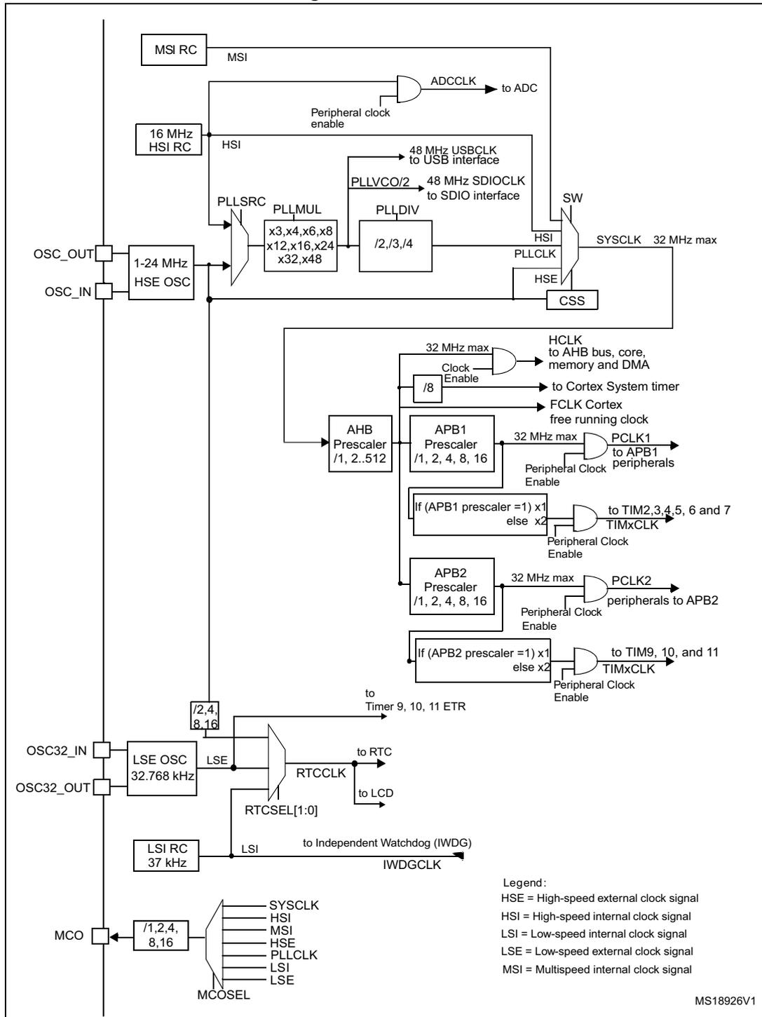
The diagram illustrates the internal clock distribution system. At the top, the MSI RC (Multispeed internal clock signal) provides the MSI clock. The 16 MHz HSI RC (High-speed internal clock signal) provides the HSI clock. The HSE OSC (High-speed external clock signal) connected to OSC_IN and OSC_OUT provides the HSE clock, which can be configured for 1-24 MHz . The LSE OSC (Low-speed external clock signal) connected to OSC32_IN and OSC32_OUT provides the LSE clock at 32.768 kHz . The LSI RC (Low-speed internal clock signal) provides the LSI clock at 37 kHz . A MCO (Microcontroller Clock Output) pin is connected to a multiplexer ( MCOSEL ) that can select between SYSCLK , HSI , MSI , HSE , PLLCLK , LSI , and LSE with prescalers of /1, /2, /4, /8, /16 . The PLL (Phase-Locked Loop) takes HSI or HSE as input ( PLL SRC ), multiplies it by PLL MUL (options: x3, x4, x6, x8, x12, x16, x24, x32, x48 ), and divides it by PLL DIV (options: /2, /3, /4 ) to generate PLLCLK . A CSS (Clock Security System) monitors the HSE clock. A SW (Switch) selects the system clock ( SYSCLK , 32 MHz max ) from HSI , HSE , or PLLCLK . The ADCCLK is derived from HSI via a Peripheral clock enable gate. The 48 MHz USBCLK to the USB interface and the 48 MHz SDIOCLK to the SDIO interface are derived from PLL VCO/2 . The HCLK (to AHB bus, core, memory and DMA) is derived from SYSCLK via an AHB Prescaler (options: /1, /2, /4, /8, /16 ). The FCLK (Cortex free running clock) is derived from HCLK via a /8 prescaler. The PCLK1 (to APB1 peripherals) is derived from HCLK via an APB1 Prescaler (options: /1, /2, /4, /8, /16 ). The TIMxCLK (to TIM2, 3, 4, 5, 6 and 7) is derived from PCLK1 via a multiplexer that selects between x1 (if APB1 prescaler = 1) or x2 (else). The PCLK2 (peripherals to APB2) is derived from HCLK via an APB2 Prescaler (options: /1, /2, /4, /8, /16 ). The TIMxCLK (to TIM9, 10, and 11) is derived from PCLK2 via a multiplexer that selects between x1 (if APB2 prescaler = 1) or x2 (else). The RTCCLK (to RTC and LCD) is derived from LSE or LSI via an RTCSEL[1:0] multiplexer. The IWDGCLK (to Independent Watchdog) is derived from LSI . The Timer 9, 10, 11 ETR is derived from HSI via a prescaler (options: /2, /4, /8, /16 ). A legend defines the clock signal types: HSE = High-speed external clock signal, HSI = High-speed internal clock signal, LSI = Low-speed internal clock signal, LSE = Low-speed external clock signal, MSI = Multispeed internal clock signal. The reference number MS18926V1 is shown in the bottom right corner.
- 1. For full details about the internal and external clock source characteristics, refer to the “Electrical characteristics” section in your device datasheet.
The timer clock frequencies are automatically fixed by hardware. There are two cases:
- 1. If the APB prescaler is 1, the timer clock frequencies are set to the same frequency as that of the APB domain to which the timers are connected.
- 2. Otherwise, they are set to twice ( \( \times 2 \) ) the frequency of the APB domain to which the timers are connected.
FCLK acts as Cortex ® -M3 free running clock. For more details refer to the Arm ® Cortex ® -M3 Technical Reference Manual.
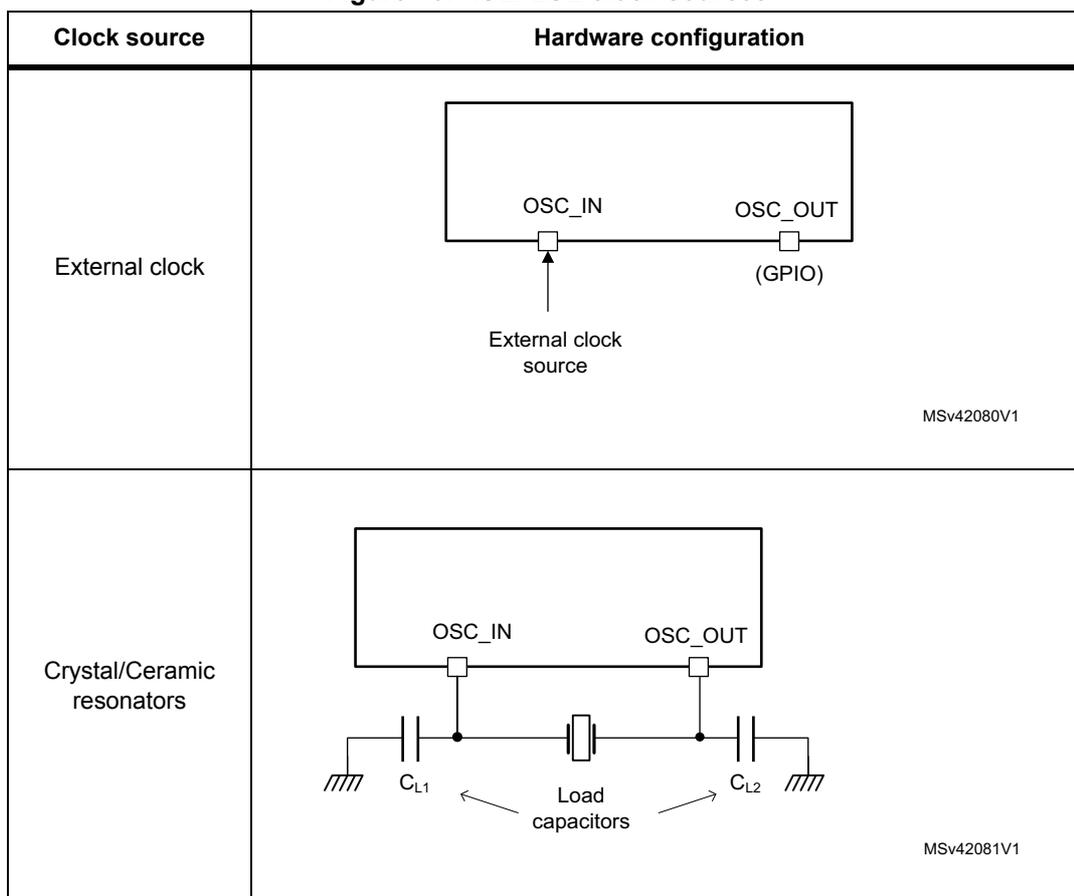
6.2.1 HSE clock
The high speed external clock signal (HSE) can be generated from two possible clock sources:
- • HSE external crystal/ceramic resonator
- • HSE user external clock
The resonator and the load capacitors have to be placed as close as possible to the oscillator pins in order to minimize output distortion and startup stabilization time. The loading capacitance values must be adjusted according to the selected oscillator.
Figure 16. HSE/ LSE clock sources
| Clock source | Hardware configuration |
|---|---|
| External clock | The diagram shows a rectangular block representing the microcontroller. It has two pins on the bottom labeled OSC_IN and OSC_OUT. An arrow labeled 'External clock source' points to the OSC_IN pin. The OSC_OUT pin is labeled '(GPIO)'. MSV42080V1 |
| Crystal/Ceramic resonators | The diagram shows a rectangular block representing the microcontroller. It has two pins on the bottom labeled OSC_IN and OSC_OUT. A crystal/ceramic resonator is connected between these two pins. Two capacitors, labeled C L1 and C L2 , are connected from the OSC_IN and OSC_OUT pins respectively to ground. An arrow labeled 'Load capacitors' points to both C L1 and C L2 . MSV42081V1 |
External source (HSE bypass)
In this mode, an external clock source must be provided. It can have a frequency of up to 32 MHz. This mode is selected by setting the HSEBYP and HSEON bits in the Clock control register, RCC_CR (see Section 6.3.1 ). The external clock signal (square, sinus or triangle) with ~50% duty cycle has to drive the OSC_IN pin while the OSC_OUT pin should be left hi-Z (see Figure 16 ).
External crystal/ceramic resonator (HSE crystal)
The 1 to 24 MHz external oscillator has the advantage of producing a very accurate rate on the main clock.
The associated hardware configuration is shown in Figure 16 . Refer to the electrical characteristics section of the datasheet for more details.
The HSERDY flag of the RCC_CR register (see Section 6.3.1 ) indicates whether the HSE oscillator is stable or not. At startup, the HSE clock is not released until this bit is set by hardware. An interrupt can be generated if enabled in the RCC_CR register .
The HSE Crystal can be switched on and off using the HSEON bit in the RCC_CR register .
6.2.2 HSI clock
The HSI clock signal is generated from an internal 16 MHz RC oscillator. It can be used directly as a system clock or as PLL input.
The HSI RC oscillator has the advantage of providing a clock source at low cost (no external components). It also has a faster startup time than the HSE crystal oscillator however, even with calibration the frequency is less accurate than an external crystal oscillator or ceramic resonator.
Calibration
RC oscillator frequencies can vary from one chip to another due to manufacturing process variations, this is why each device is factory calibrated by ST for 1% accuracy at an ambient temperature, T A , of 30 °C.
After reset, the factory calibration value is loaded in the HSICAL[7:0] bits in the Internal Clock Sources Calibration Register (RCC_ICSCR) (see Section 6.3.2 ).
If the application is subject to voltage or temperature variations, this may affect the RC oscillator speed. You can trim the HSI frequency in the application by using the HSITRIM[4:0] bits in the RCC_ICSCR register . The default HSITRIM value is 16, which trims the HSI oscillator to nominal frequency of 16 MHz. An increase of the HSITRIM value is causing increase of HSI oscillator frequency. The trimming step (F HSITRIM ) is around 40 kHz between two consecutive HSICAL steps. The frequency response on the trimming code change shows non-monotonicity if the trimming code is a multiple of 16, see device datasheet for details. For more details on how to measure the HSI frequency variation refer to Section 6.2.14: Internal/external clock measurement with TIM9/TIM10/TIM11 .
The HSIRDY flag in the RCC_CR indicates whether the HSI oscillator is stable or not. At startup, the HSI RC output clock is not released until this bit is set by hardware.
The HSI RC oscillator can be switched on and off using the HSION bit in the RCC_CR register .
6.2.3 MSI clock
The MSI clock signal is generated from an internal RC oscillator. Its frequency range can be adjusted by software by using the MSIRANGE[2:0] bits in the RCC_ICSCR register (see Section 6.3.2: Internal clock sources calibration register (RCC_ICSCR) ). Seven frequency ranges are available: 65.536 kHz, 131.072 kHz, 262.144 kHz, 524.288 kHz, 1.048 MHz, 2.097 MHz (default value) and 4.194 MHz.
The MSI clock is used as system clock after restart from Reset, wake-up from Stop, and Standby low-power mode. After restart from Reset or wake-up from Standby, the MSI frequency is set to its default value. The RCC_ICSCR register value is retained in STOP mode, thus the MSI frequency and calibration after Wake-Up is the same as before entering STOP mode.
The MSI RC oscillator has the advantage of providing a low-cost (no external components) low-power clock source. It is used as wake-up clock in low-power modes to reduce power consumption and wake-up time.
The MSIRDY flag in the RCC_CR register indicates whether the MSI RC is stable or not. At startup, the MSI RC output clock is not released until this bit is set by hardware.
The MSI RC can be switched on and off by using the MSION bit in the RCC_CR register (see Section 6.3.1 ).
It can also be used as a backup clock source (auxiliary clock) if the HSE crystal oscillator fails. Refer to Section 6.2.9: Clock security system (CSS) on page 134 .
Calibration
The MSI RC oscillator frequency can vary from one chip to another due to manufacturing process variations, this is why each device is factory calibrated by ST for 1% accuracy at an ambient temperature, \( T_A \) , of 30 °C.
After reset, the factory calibration value is loaded in the MSICAL[7:0] bits in the RCC_ICSCR register. If the application is subject to voltage or temperature variations, this may affect the RC oscillator speed. You can trim the MSI frequency in the application by using the MSITRIM[7:0] bits in the RCC_ICSCR register. For more details on how to measure the MSI frequency variation refer to Section 6.2.14: Internal/external clock measurement with TIM9/TIM10/TIM11 .
6.2.4 PLL
The internal PLL can be clocked by the HSI RC or HSE crystal. It is used to drive the system clock and to generate the 48 MHz clock for the USB peripheral (refer to Figure 15 and Section 6.3.1: Clock control register (RCC_CR) ).
The PLL input clock frequency must be between 2 and 24 MHz.
The desired frequency is obtained by using the multiplication factor and output division embedded in the PLL:
- • If the USB or SDIO interface is used in the application, the PLL VCO clock (defined by the PLL multiplication factor) must be programmed to output a 96 MHz frequency. This is required to provide a 48 MHz clock to the USB or SDIO (SDIOCLK or USBCLK = PLLVCO/2).
- • The system clock is derived from the PLL VCO divided by the output division factor.
Note:
The application software must set correctly the PLL multiplication factor to avoid exceeding 96 MHz as PLLVCO when the product is in range 1, 48 MHz as PLLVCO when the product is in range 2, 24 MHz when the product is in range 3.
It must also set correctly the output division to avoid exceeding 32 MHz as SYSCLK.
The minimum input clock frequency for PLL is 2 MHz (when using HSE as PLL source).
The PLL configuration (selection of the source clock, multiplication factor and output division factor) must be performed before enabling the PLL. Once the PLL is enabled, these parameters cannot be changed.
To modify the PLL configuration, proceed as follows:
- 1. Disable the PLL by setting PLLON to 0.
- 2. Wait until PLLRDY is cleared. PLLRDY. The PLL is now fully stopped.
- 3. Change the desired parameter.
- 4. Enable the PLL again by setting PLLON to 1.
An interrupt can be generated when the PLL is ready if enabled in the RCC_CIR register (see Section 6.3.4 ).
6.2.5 LSE clock
The LSE crystal is a 32.768 kHz low speed external crystal or ceramic resonator. It has the advantage of providing a low-power but highly accurate clock source to the real-time clock peripheral (RTC) for clock/calendar or other timing functions.
The LSE crystal is switched on and off using the LSEON bit in the RCC_CSR register (see Section 6.3.14 ).
The LSERDY flag in the RCC_CSR register indicates whether the LSE crystal is stable or not. At startup, the LSE crystal output clock signal is not released until this bit is set by hardware. An interrupt can be generated if enabled in the RCC_CIR register (see Section 6.3.4 ).
External source (LSE bypass)
In this mode, an external clock source must be provided. It can have a frequency of up to 1 MHz. This mode is selected by setting the LSEBYP and LSEON bits in the RCC_CR (see Section 6.3.1 ). The external clock signal (square, sinus or triangle) with ~50% duty cycle has to drive the OSC32_IN pin while the OSC32_OUT pin might be used as a GPIO pin (see Figure 16 ).
6.2.6 LSI clock
The LSI RC acts as an low-power clock source that can be kept running in Stop and Standby mode for the independent watchdog (IWDG). The clock frequency is around 37 kHz.
The LSI RC oscillator can be switched on and off using the LSION bit in the RCC_CSR register (see Section 6.3.14 ), but the LSI oscillator keeps running since it is activated by IWDG.
The LSIRDY flag in RCC_CSR indicates whether the low-speed internal oscillator is stable or not. At startup, the clock is not released until this bit is set by hardware. An interrupt can be generated if enabled in the RCC_CIR (see Section 6.3.4 ).
LSI measurement
The frequency dispersion of the LSI oscillator can be measured to have accurate RTC time base and/or IWDG timeout (when LSI is used as clock source for these peripherals) with an acceptable accuracy. For more details, refer to the electrical characteristics section of the datasheets. For more details on how to measure the LSI frequency, refer to Section 6.2.14: Internal/external clock measurement with TIM9/TIM10/TIM11 .
6.2.7 System clock (SYSCLK) selection
Four different clock sources can be used to drive the system clock (SYSCLK):
- • The HSI oscillator
- • The HSE oscillator
- • The PLL
- • The MSI oscillator clock (default after reset)
When a clock source is used directly or through the PLL as system clock, it is not possible to stop it.
A switch from one clock source to another occurs only if the target clock source is ready (clock stable after startup delay or PLL locked). If a clock source which is not yet ready is selected, the switch occurs when the clock source is ready. Status bits in the RCC_CR register indicate which clock(s) is (are) ready and which clock is currently used as system clock.
Note: The SYSCLK frequency change has to follow the rule that the final frequency is less than 4 x initial frequency to limit the VCORE drop due to a current consumption peak when the frequency increases. It must also respect 5 µs delay between two changes.
For example to switch from 4.2 MHz to 32 MHz, the user can switch from 4.2 MHz to 16 MHz, wait 5 µs, then switch from 16 MHz to 32 MHz.
6.2.8 System clock source frequency versus voltage range
The following table gives the different clock source frequencies depending on the product voltage range.
Table 35. System clock source frequency
| Product voltage range | Clock frequency | |||
|---|---|---|---|---|
| MSI | HSI | HSE | PLL | |
| Range 1 (1.8 V) | 4.2 MHz | 16 MHz | HSE 32 MHz (external clock) or 24 MHz (crystal) | 32 MHz (PLLVC0 max = 96 MHz) |
| Range 2 (1.5 V) | 4.2 MHz | 16 MHz | 16 MHz | 16 MHz (PLLVC0 max = 48 MHz) |
| Range 3 (1.2 V) | 4.2 MHz | NA | 8 MHz | 4 MHz (PLLVC0 max = 24 MHz) |
6.2.9 Clock security system (CSS)
The Clock security system can be activated by software. In this case, the clock detector is enabled after the HSE oscillator startup delay, and disabled when this oscillator is stopped.
If a failure is detected on the HSE clock, this oscillator is automatically disabled and an interrupt is generated to inform the software about the failure (Clock Security System Interrupt, CSSI), allowing the MCU to perform rescue operations. The CSSI is linked to the Cortex®-M3 NMI (Non-Maskable Interrupt) exception vector.
Note: Once the CSS is enabled and if the HSE clock fails, the CSS interrupt occurs and an NMI is automatically generated. The NMI is executed indefinitely unless the CSS interrupt pending bit is cleared. As a consequence, in the NMI ISR must clear the CSS interrupt by setting the CSSC bit in the RCC_CIR register.
If the HSE oscillator is used directly or indirectly as the system clock (indirectly means: it is used as PLL input clock, and the PLL clock is used as system clock), a detected failure causes a switch of the system clock to the MSI oscillator and the disabling of the HSE oscillator. If the HSE oscillator clock is the clock entry of the PLL used as system clock when the failure occurs, the PLL is disabled too.
6.2.10 Clock Security System on LSE
In Cat.2, Cat.3, Cat.4, Cat.5 and Cat.6 devices, a Clock Security System on LSE can be activated by software writing the LSECSSON bit in the RCC_CSR register. This bit can be disabled only by a hardware reset or RTC software reset, or after a failure detection on LSE. LSECSSON must be written after LSE and LSI are enabled (LSEON and LSION enabled) and ready (LSERDY and LSIRDY set by hardware), and after the RTC clock has been selected by RTCSEL.
If the CSS failure is detected on the external LSE oscillator the LSECSSD flag is set. The failure event is linked to EXTI line 19. It can wakeup MCU from Standby mode or rise an interrupt which can be used to service the failure event in the TAMPER_STAMP interrupt routine in run, Sleep and Stop low-power modes.
To enable interrupt generation, the LSECSIE bit in RCC_CIR interrupt register has to be set (see Section 6.3.4: Clock interrupt register (RCC_CIR) on page 144 ).
In case of the CSS failure, the LSE clock is no longer supplied to the RTC and fail-safe mode needs to be managed by the firmware (stop the LSE oscillator and switch RTC clock source to LSI or HSE clock).
The frequency of LSE oscillator have to be higher than 30 kHz to avoid false positive CSS detection.
6.2.11 RTC and LCD clock
The RTC and LCD have the same clock source which can be either the LSE, the LSI, or the HSE 1 MHz clock (HSE divided by a programmable prescaler). It is selected by programming the RTCSEL[1:0] bits in the RCC_CSR register (see Section 6.3.14 ) and the RTCPRE[1:0] bits in the RCC_CR register (see Section 6.3.1 ).
Once the RTC and LCD clock source have been selected, the only possible way of modifying the selection is to set the RTCRST bit in the RCC_CSR register, or by a POR.
If the LSE or LSI is used as RTC clock source, the RTC continues to work in Stop and Standby low-power modes, and can be used as wakeup source. However, when the HSE is the RTC clock source, the RTC cannot be used in the Stop and Standby low-power modes. The LCD can however be used in the Stop low-power mode if the LSE or LSI is used as the RTC clock source.
When the RTC clock is LSE, the RTC remains clocked and functional under system reset.
Note: To be able to read the RTC calendar register when the APB1 clock frequency is less than seven times the RTC clock frequency ( \( 7 \times \text{RTCLCK} \) ), the software must read the calendar time and date registers twice.
If the second read of the RTC_TR gives the same result as the first read, this ensures that the data is correct. Otherwise a third read access must be done.
6.2.12 Watchdog clock
If the Independent watchdog (IDG) is started by either hardware option or software access, the LSI oscillator is forced ON and cannot be disabled. After the LSI oscillator temporization, the clock is provided to the IWDG.
6.2.13 Clock-out capability
The microcontroller clock output (MCO) capability allows the clock to be output onto the external MCO pin (PA8) using a configurable prescaler (1, 2, 4, 8, or 16). The configuration registers of the corresponding GPIO port must be programmed in alternate function mode. One of 7 clock signals can be selected as the MCO clock:
- • SYSCLK
- • HSI
- • MSI
- • HSE
- • PLL
- • LSI
- • LSE
The selection is controlled by the MCOSEL[2:0] bits of the RCC_CFGR register (see Section 6.3.3 ).
6.2.14 Internal/external clock measurement with TIM9/TIM10/TIM11
It is possible to indirectly measure the frequency of all on-board clock source generators by means of the TIM9/TIM10/TIM11 channel 1 input capture, as represented on Figure 17 .
Figure 17. Using the TIM9/TIM10/TIM11 channel 1 input capture to measure frequencies
![Diagram showing the input capture configuration for TIM9, TIM10, and TIM11. Each timer has an input multiplexer for its TI(1) pin. TIM9's TI(1) can be connected to a GPIO or ETR. TIM10's TI(1) can be connected to a GPIO, RTC_WakeUp_IT, LSE, or LSI. TIM11's TI(1) can be connected to a GPIO, MSI, or HSE_RTC (1 MHz). Each multiplexer is controlled by TI1_RMP[1:0] bits in the TIMx_OR register. ETR pins for all three timers are connected to a common GPIO line.](/RM0038-STM32L100-151-152-162/3334fcca5dac808f4fd3840aba35bc2e_img.jpg)
The diagram illustrates the input capture configuration for three timers: TIM9, TIM10, and TIM11. Each timer has an input multiplexer for its TI(1) pin. The multiplexers are controlled by the TI1_RMP[1:0] bits in the TIMx_OR register. The connections are as follows:
- TIM9: The TI(1) pin is connected to a multiplexer that selects between a GPIO and the ETR pin. The ETR pin is connected to a common GPIO line.
- TIM10: The TI(1) pin is connected to a multiplexer that selects between a GPIO, RTC_WakeUp_IT, LSE, and LSI. The ETR pin is connected to the same common GPIO line.
- TIM11: The TI(1) pin is connected to a multiplexer that selects between a GPIO, MSI, and HSE_RTC (1 MHz). The ETR pin is connected to the same common GPIO line.
The common GPIO line for the ETR pins is connected to a GPIO block. The TI1_RMP[1:0] bits for each timer are shown as control inputs to their respective multiplexers.
MS33423V1
Each timer has an input multiplexer that selects which of the I/O or the internal clock is to trigger the input capture. This selection is performed through the TI1_RMP [1:0] bits in the TIMx_OR register.
For TIM9 and TIM10, the primary purpose of connecting the LSE to the channel 1 input capture is to be able to precisely measure the HSI and MSI system clocks (for this, either the HSI or MSI should be used as the system clock source). The number of HSI (MSI, respectively) clock counts between consecutive edges of the LSE signal provides a measure of the internal clock period. Taking advantage of the high precision of LSE crystals (typically a few tens of ppm's), it is possible to determine the internal clock frequency with the same resolution, and trim the source to compensate for manufacturing-process- and/or temperature- and voltage-related frequency deviations.
The MSI and HSI oscillators both have dedicated user-accessible calibration bits for this purpose.
The basic concept consists in providing a relative measurement (e.g. the HSI/LSE ratio): the precision is therefore closely related to the ratio between the two clock sources. The higher the ratio, the better the measurement.
It is however not possible to have a good enough resolution when the MSI clock is low (typically below 1 MHz). In this case, it is advised to:
- • accumulate the results of several captures in a row
- • use the timer's input capture prescaler (up to 1 capture every 8 periods)
- • use the RTC wakeup interrupt signal (when the RTC is clocked by the LSE) as the input for the channel1 input capture. This improves the measurement precision. For this purpose the RTC wakeup interrupt must be enabled.
TIM10 can also be used to measure the LSI: this is useful for applications with no crystal. The ultra-low-power LSI oscillator has a wide manufacturing process deviation: by measuring it as a function of the HSI clock source, it is possible to determine its frequency with the precision of the HSI.
Finally, TIM11 has two other sources. TIM11 can use the MSI just like TIM10 uses the LSI for crystal-less applications. The HSE_RTC frequency (HSE divided by a programmable prescaler) being relatively high (1MHz), the relative frequency measurement is not very precise, so its main purpose is to have a rough indication of the external crystal frequency. This is useful for instance to meet the requirements of the IEC 60730/IEC 61335 standards, which requires to be able to determine harmonic or subharmonic frequencies (-50/+100% deviations).
6.2.15 Clock-independent system clock sources for TIM9/TIM10/TIM11
In a number of applications using the 32.768 kHz clock as a time base for the RTC, it is interesting to have time bases that work completely independently of the system clock. This allows the scheduling of tasks without having to take into account the processor state (the processor may be stopped or executing at low, medium or full speed).
For this purpose, the LSE clock is internally redirected to the 3 timers' ETR inputs, which are used as additional clock sources, as shown in Figure 17 on page 137 . This gives up to three independent time bases (using the auto-reload feature) with 1 or 2 compare additional channels for fractional events. For instance, the TIM9's auto-reload interrupt can be programmed for a 1 second tick interrupt with an additional interrupt occurring 250 ms after the main tick.
Note: In this configuration, make sure that you have at least a ratio of 2 between the external clock (LSE) and the APB clock. If the application uses an APB clock frequency lower than twice the LSE clock frequency (typically LSE = 32.768 kHz, so twice LSE = 65.536 kHz), it is mandatory to use the external trigger prescaler feature of the timer: it can divide the ETR clock by up to 8.
6.3 RCC registers
Refer to Section 1.2 for a list of abbreviations used in register descriptions.
6.3.1 Clock control register (RCC_CR)
Address offset: 0x00
Reset value: 0b0XX0 0000 0000 0X00 0000 0011 0000 0000 where X is undefined
Access: no wait state, word, half-word and byte access
| 31 | 30 | 29 | 28 | 27 | 26 | 25 | 24 | 23 | 22 | 21 | 20 | 19 | 18 | 17 | 16 |
|---|---|---|---|---|---|---|---|---|---|---|---|---|---|---|---|
| Res. | RTCPRE[1:0] | CSS ON | Reserved | PLL RDY | PLLON | Reserved | HSE BYP | HSE RDY | HSE ON | ||||||
| rw | rw | rw | r | rw | rw | r | rw | ||||||||
| 15 | 14 | 13 | 12 | 11 | 10 | 9 | 8 | 7 | 6 | 5 | 4 | 3 | 2 | 1 | 0 |
| Reserved | MSI RDY | MSION | Reserved | HSI RDY | HSION | ||||||||||
| r | rw | r | rw | ||||||||||||
Bit 31 Reserved, must be kept at reset value.
Bits 30:29 RTCPRE[1:0] RTC/LCD prescaler
These bits are set and reset by software to obtain a 1 MHz clock from HSE. This prescaler cannot be modified if HSE is enabled (HSEON = 1).
These bits are reset by power on reset, they keep their value after system reset.
00: HSE is divided by 2 for RTC/LCD clock
01: HSE is divided by 4 for RTC/LCD clock
10: HSE is divided by 8 for RTC/LCD clock
11: HSE is divided by 16 for RTC/LCD clock
Bit 28 CSSON : Clock security system enable
This bit is set and cleared by software to enable the clock security system (CSS). When CSSON is set, the clock detector is enabled by hardware when the HSE oscillator is ready, and disabled by hardware if an oscillator failure is detected.
0: Clock security system OFF (clock detector OFF)
1: Clock security system ON (clock detector ON if HSE oscillator is stable, OFF otherwise)
Bits 27:26 Reserved, must be kept at reset value.
Bit 25 PLL RDY : PLL clock ready flag
This bit is set by hardware to indicate that the PLL is locked.
0: PLL unlocked
1: PLL locked
Bit 24 PLLON : PLL enable
This bit is set and cleared by software to enable PLL.
Cleared by hardware when entering Stop or Standby mode. This bit can not be reset if the PLL clock is used as system clock or is selected to become the system clock.
0: PLL OFF
1: PLL ON
Bits 23:19 Reserved, must be kept at reset value.
Bit 18 HSEBYP: HSE clock bypassThis bit is set and cleared by software to bypass the oscillator with an external clock. The external clock must be enabled with the HSEON bit, to be used by the device.
The HSEBYP bit can be written only if the HSE oscillator is disabled.
This bit is reset by power on reset, it keeps its value after system reset.
0: HSE oscillator not bypassed
1: HSE oscillator bypassed with an external clock
Bit 17 HSERDY: HSE clock ready flagThis bit is set by hardware to indicate that the HSE oscillator is stable. After the HSEON bit is cleared, HSERDY goes low after 6 HSE oscillator clock cycles.
0: HSE oscillator not ready
1: HSE oscillator ready
Bit 16 HSEON: HSE clock enableThis bit is set and cleared by software.
Cleared by hardware to stop the HSE oscillator when entering Stop or Standby mode. This bit cannot be reset if the HSE oscillator is used directly or indirectly as the system clock.
0: HSE oscillator OFF
1: HSE oscillator ON
Bits 15:10 Reserved, must be kept at reset value.
Bit 9 MSIRDY: MSI clock ready flagThis bit is set by hardware to indicate that the MSI oscillator is stable.
0: MSI oscillator not ready
1: MSI oscillator ready
Note: Once the MSION bit is cleared, MSIRDY goes low after 6 MSI clock cycles.
Bit 8 MSION: MSI clock enableThis bit is set and cleared by software.
Set by hardware to force the MSI oscillator ON when exiting from Stop or Standby mode, or in case of a failure of the HSE oscillator used directly or indirectly as system clock. This bit cannot be cleared if the MSI is used as system clock.
0: MSI oscillator OFF
1: MSI oscillator ON
Bits 7:2 Reserved, must be kept at reset value.
Bit 1 HSIRDY: Internal high-speed clock ready flagThis bit is set by hardware to indicate that the HSI oscillator is stable. After the HSION bit is cleared, HSIRDY goes low after 6 HSI clock cycles.
0: HSI oscillator not ready
1: HSI oscillator ready
Bit 0 HSION: Internal high-speed clock enableThis bit is set and cleared by software.
This bit cannot be cleared if the HSI is used directly or indirectly as the system clock.
0: HSI oscillator OFF
1: HSI oscillator ON
6.3.2 Internal clock sources calibration register (RCC_ICSCR)
Address offset: 0x04
Reset value: 0x00XX B0XX where X is undefined.
Access: no wait state, word, half-word and byte access
| 31 | 30 | 29 | 28 | 27 | 26 | 25 | 24 | 23 | 22 | 21 | 20 | 19 | 18 | 17 | 16 |
|---|---|---|---|---|---|---|---|---|---|---|---|---|---|---|---|
| MSITRIM[7:0] | MSICAL[7:0] | ||||||||||||||
| rw | rw | rw | rw | rw | rw | rw | rw | r | r | r | r | r | r | r | r |
| 15 | 14 | 13 | 12 | 11 | 10 | 9 | 8 | 7 | 6 | 5 | 4 | 3 | 2 | 1 | 0 |
| MSIRANGE[2:0] | HSITRIM[4:0] | HSICAL[7:0] | |||||||||||||
| rw | rw | rw | rw | rw | rw | rw | rw | r | r | r | r | r | r | r | r |
Bits 31:24 MSITRIM[7:0]: MSI clock trimming
These bits are set by software to adjust MSI calibration.
These bits provide an additional user-programmable trimming value that is added to the MSICAL[7:0] bits. They can be programmed to compensate for the variations in voltage and temperature that influence the frequency of the internal MSI RC.
Bits 23:16 MSICAL[7:0]: MSI clock calibration
These bits are initialized at startup with the factory-programmed MSI calibration trim value. When MSITRIM is written, MSICAL is updated with the sum of MSITRIM and the factory trim value.
Bits 15:13 MSIRANGE[2:0]: MSI clock ranges
These bits are set by software to choose the frequency range of MSI. 7 frequency ranges are available:
- 000: range 0 around 65.536 kHz
- 001: range 1 around 131.072 kHz
- 010: range 2 around 262.144 kHz
- 011: range 3 around 524.288 kHz
- 100: range 4 around 1.048 MHz
- 101: range 5 around 2.097 MHz (reset value)
- 110: range 6 around 4.194 MHz
- 111: not allowed
Bits 12:8 HSITRIM[4:0]: High speed internal clock trimming
These bits provide an additional user-programmable trimming value that is added to the HSICAL[7:0] bits. They can be programmed to compensate for the variations in voltage and temperature that influence the frequency of the internal HSI RC.
Bits 7:0 HSICAL[7:0]: Internal high speed clock calibration
These bits are initialized at startup with the factory-programmed HSI calibration trim value. When HSITRIM is written, HSICAL is updated with the sum of HSITRIM and the factory trim value.
6.3.3 Clock configuration register (RCC_CFGR)
Address offset: 0x08
Reset value: 0x0000 0000
Access: 0 ≤ wait state ≤ 2, word, half-word and byte access
1 or 2 wait states inserted only if the access occurs during clock source switch.
| 31 | 30 | 29 | 28 | 27 | 26 | 25 | 24 | 23 | 22 | 21 | 20 | 19 | 18 | 17 | 16 |
|---|---|---|---|---|---|---|---|---|---|---|---|---|---|---|---|
| Res. | MCOPRE[2:0] | Res. | MCOSEL[2:0] | PLLDIV[1:0] | PLLMUL[3:0] | Res. | PLL SRC | ||||||||
| rw | rw | rw | rw | rw | rw | rw | rw | rw | rw | rw | rw | rw | |||
| 15 | 14 | 13 | 12 | 11 | 10 | 9 | 8 | 7 | 6 | 5 | 4 | 3 | 2 | 1 | 0 |
| Reserved | PPRE2[2:0] | PPRE1[2:0] | HPRE[3:0] | SWS[1:0] | SW[1:0] | ||||||||||
| rw | rw | rw | rw | rw | rw | rw | rw | rw | rw | r | r | rw | rw | rw | |
Bits 31 Reserved, must be kept at reset value.
Bits 30:28 MCOPRE[2:0] : Microcontroller clock output prescaler
These bits are set and cleared by software.
It is highly recommended to change this prescaler before MCO output is enabled.
000: MCO is divided by 1
001: MCO is divided by 2
010: MCO is divided by 4
011: MCO is divided by 8
100: MCO is divided by 16
Others: not allowed
Bits 27 Reserved, must be kept at reset value.
Bits 26:24 MCOSEL[2:0] : Microcontroller clock output selection
These bits are set and cleared by software.
000: MCO output disabled, no clock on MCO
001: SYSCLK clock selected
010: HSI oscillator clock selected
011: MSI oscillator clock selected
100: HSE oscillator clock selected
101: PLL clock selected
110: LSI oscillator clock selected
111: LSE oscillator clock selected
Note: This clock output may have some truncated cycles at startup or during MCO clock source switching.
Bits 23:22 PLLDIV[1:0] : PLL output division
These bits are set and cleared by software to control PLL output clock division from PLL VCO clock. These bits can be written only when the PLL is disabled.
00: not allowed
01: PLL clock output = PLLVCO / 2
10: PLL clock output = PLLVCO / 3
11: PLL clock output = PLLVCO / 4
Bits 21:18 PLLMUL[3:0] : PLL multiplication factorThese bits are written by software to define the PLL multiplication factor to generate the PLL VCO clock. These bits can be written only when the PLL is disabled.
0000: PLLVCO = PLL clock entry x 3
0001: PLLVCO = PLL clock entry x 4
0010: PLLVCO = PLL clock entry x 6
0011: PLLVCO = PLL clock entry x 8
0100: PLLVCO = PLL clock entry x 12
0101: PLLVCO = PLL clock entry x 16
0110: PLLVCO = PLL clock entry x 24
0111: PLLVCO = PLL clock entry x 32
1000: PLLVCO = PLL clock entry x 48
others: not allowed
Caution: The PLL VCO clock frequency must not exceed 96 MHz when the product is in Range 1, 48 MHz when the product is in Range 2 and 24 MHz when the product is in Range 3.
Bit 17 Reserved, must be kept at reset value.
Bit 16 PLL SRC : PLL entry clock sourceThis bit is set and cleared by software to select PLL clock source. This bit can be written only when PLL is disabled.
0: HSI oscillator clock selected as PLL input clock
1: HSE oscillator clock selected as PLL input clock
Note: The PLL minimum input clock frequency is 2 MHz.
Bits 15:14 Reserved, must be kept at reset value.
Bits 13:11 PPRE2[2:0] : APB high-speed prescaler (APB2)These bits are set and cleared by software to control the division factor of the APB high-speed clock (PCLK2).
0xx: HCLK not divided
100: HCLK divided by 2
101: HCLK divided by 4
110: HCLK divided by 8
111: HCLK divided by 16
These bits are set and cleared by software to control the division factor of the APB low-speed clock (PCLK1).
0xx: HCLK not divided
100: HCLK divided by 2
101: HCLK divided by 4
110: HCLK divided by 8
111: HCLK divided by 16
Bits 7:4 HPRE[3:0] : AHB prescaler
These bits are set and cleared by software to control the division factor of the AHB clock.
Caution: Depending on the device voltage range, the software has to set correctly these bits to ensure that the system frequency does not exceed the maximum allowed frequency (for more details refer to the Dynamic voltage scaling management section in the PWR chapter.) After a write operation to these bits and before decreasing the voltage range, this register must be read to be sure that the new value has been taken into account.
- 0xxx: SYSCLK not divided
- 1000: SYSCLK divided by 2
- 1001: SYSCLK divided by 4
- 1010: SYSCLK divided by 8
- 1011: SYSCLK divided by 16
- 1100: SYSCLK divided by 64
- 1101: SYSCLK divided by 128
- 1110: SYSCLK divided by 256
- 1111: SYSCLK divided by 512
Bits 3:2 SWS[1:0] : System clock switch status
These bits are set and cleared by hardware to indicate which clock source is used as system clock.
- 00: MSI oscillator used as system clock
- 01: HSI oscillator used as system clock
- 10: HSE oscillator used as system clock
- 11: PLL used as system clock
Bits 1:0 SW[1:0] : System clock switch
These bits are set and cleared by software to select SYSCLK source.
Set by hardware to force MSI selection when leaving Stop and Standby mode or in case of failure of the HSE oscillator used directly or indirectly as system clock (if the Clock Security System is enabled).
- 00: MSI oscillator used as system clock
- 01: HSI oscillator used as system clock
- 10: HSE oscillator used as system clock
- 11: PLL used as system clock
6.3.4 Clock interrupt register (RCC_CIR)
Address offset: 0x0C
Reset value: 0x0000 0000
Access: no wait state, word, half-word and byte access
| 31 | 30 | 29 | 28 | 27 | 26 | 25 | 24 | 23 | 22 | 21 | 20 | 19 | 18 | 17 | 16 |
|---|---|---|---|---|---|---|---|---|---|---|---|---|---|---|---|
| Reserved | CSSC | LSECS SC | MSI RDYC | PLL RDYC | HSE RDYC | HSI RDYC | LSE RDYC | LSI RDYC | |||||||
| w | w | w | w | w | w | w | w | ||||||||
| 15 | 14 | 13 | 12 | 11 | 10 | 9 | 8 | 7 | 6 | 5 | 4 | 3 | 2 | 1 | 0 |
| Res. | LSECS SIE | MSI RDYIE | PLL RDYIE | HSE RDYIE | HSI RDYIE | LSE RDYIE | LSI RDYIE | CSSF | LSE CSSF | MSI RDYF | PLL RDYF | HSE RDYF | HSI RDYF | LSE RDYF | LSI RDYF |
| rw | rw | rw | rw | rw | rw | rw | r | r | r | r | r | r | r | r | |
Bits 31:24 Reserved, must be kept at reset value.
Bit 23 CSSC : Clock security system interrupt clear
This bit is set by software to clear the CSSF flag.
0: No effect
1: Clear CSSF flag
Bit 22 LSECSSC : LSE CSS interrupt clear
Set by software to clear LSECSSF. Reset by hardware when clear done.
0: LSECSSF not cleared
1: LSECSSF cleared
Note: This bit is available in Cat.2, Cat.3, Cat.4, Cat.5 and Cat.6 devices only.
Bit 21 MSIRDYC : MSI ready interrupt clear
This bit is set by software to clear the MSIRDYF flag.
0: No effect
1: MSIRDYF cleared
Bit 20 PLLRDYC : PLL ready interrupt clear
This bit is set by software to clear the PLLRDYF flag.
0: No effect
1: PLLRDYF cleared
Bit 19 HSERDYC : HSE ready interrupt clear
This bit is set by software to clear the HSERDYF flag.
0: No effect
1: HSERDYF cleared
Bit 18 HSIRDYC : HSI ready interrupt clear
This bit is set software to clear the HSIRDYF flag.
0: No effect
1: HSIRDYF cleared
Bit 17 LSERDYC : LSE ready interrupt clear
This bit is set by software to clear the LSERDYF flag.
0: No effect
1: LSERDYF cleared
Bit 16 LSIRDYC : LSI ready interrupt clear
This bit is set by software to clear the LSIRDYF flag.
0: No effect
1: LSIRDYF cleared
Bit 15 Reserved, must be kept at reset value.
Bit 14 LSECSSIE : LSE CSS interrupt enable
Set and reset by software to enable/disable interrupts from the Clock Security System on external 32 kHz oscillator (LSE).
0: LSE CSS interrupt disabled
1: LSE CSS interrupt enabled
Note: This bit is available in Cat.2, Cat.3, Cat.4, Cat.5 and Cat.6 devices only.
Bit 13 MSIRDYIE : MSI ready interrupt enable
This bit is set and cleared by software to enable/disable interrupt caused by the MSI oscillator stabilization.
0: MSI ready interrupt disabled
1: MSI ready interrupt enabled
Bit 12 PLLREADYE : PLL ready interrupt enableThis bit is set and cleared by software to enable/disable interrupt caused by PLL lock.
0: PLL lock interrupt disabled
1: PLL lock interrupt enabled
Bit 11 HSERDYIE : HSE ready interrupt enableThis bit is set and cleared by software to enable/disable interrupt caused by the HSE oscillator stabilization.
0: HSE ready interrupt disabled
1: HSE ready interrupt enabled
Bit 10 HSIRDYIE : HSI ready interrupt enableThis bit is set and cleared by software to enable/disable interrupt caused by the HSI oscillator stabilization.
0: HSI ready interrupt disabled
1: HSI ready interrupt enabled
Bit 9 LSERDYIE : LSE ready interrupt enableThis bit is set and cleared by software to enable/disable interrupt caused by the LSE oscillator stabilization.
0: LSE ready interrupt disabled
1: LSE ready interrupt enabled
Bit 8 LSIRDYIE : LSI ready interrupt enableThis bit is set and cleared by software to enable/disable interrupt caused by LSI oscillator stabilization.
0: LSI ready interrupt disabled
1: LSI ready interrupt enabled
Bit 7 CSSF : Clock security system interrupt flagThis bit is set by hardware when a failure is detected in the HSE oscillator.
It is cleared by software by setting the CSSC bit.
0: No clock security interrupt caused by HSE clock failure
1: Clock security interrupt caused by HSE clock failure
Bit 6 LSECSSF LSE CSS Interrupt flagReset by software by writing to the LSECSSC bit. Set by hardware when a failure is detected on the external 32 KHz oscillator and the LSECSSIE bit is set.
0: No failure detected on the external 32 KHz oscillator (LSE)
1: A failure is detected on the external 32 kHz oscillator (LSE)
Note: This bit is available in Cat.2, Cat.3, Cat.4, Cat.5 and Cat.6 devices only.
Bit 5 MSIRDYF : MSI ready interrupt flagThis bit is set by hardware when the MSI becomes stable and MSIRDYIE is set.
It is cleared by software setting the MSIRDYC bit.
0: No clock ready interrupt caused by the MSI
1: Clock ready interrupt caused by the MSI
Bit 4 PLLREADYF : PLL ready interrupt flagThis bit is set by hardware when the PLL locks and PLLREADYIE is set.
It is cleared by software setting the PLLRDYC bit.
0: No clock ready interrupt caused by PLL lock
1: Clock ready interrupt caused by PLL lock
Bit3 HSERDYF : HSE ready interrupt flag
This bit is set by hardware when HSE becomes stable and HSERDYDIE is set.
It is cleared by software setting the HSERDYC bit.
0: No clock ready interrupt caused by the HSE
1: Clock ready interrupt caused by the HSE
Bit 2 HSIRDYF : HSI ready interrupt flag
This bit is set by hardware when the HSI becomes stable and HSIRDYDIE is set.
It is cleared by software setting the HSIRDYC bit.
0: No clock ready interrupt caused by the HSI
1: Clock ready interrupt caused by the HSI
Bit 1 LSERDYF : LSE ready interrupt flag
This bit is set by hardware when the LSE becomes stable and LSERDYDIE is set.
It is cleared by software setting the LSERDYC bit.
0: No clock ready interrupt caused by the LSE
1: Clock ready interrupt caused by the LSE
Bit 0 LSIRDYF : LSI ready interrupt flag
This bit is set by hardware when the LSI becomes stable and LSIRDYDIE is set.
It is cleared by software setting the LSIRDYC bit.
0: No clock ready interrupt caused by the LSI
1: Clock ready interrupt caused by the LSI
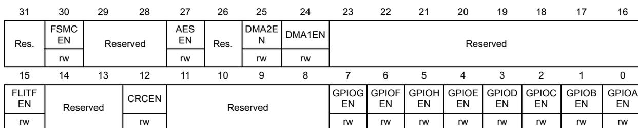
6.3.5 AHB peripheral reset register (RCC_AHBRSTR)
Address offset: 0x10
Reset value: 0x0000 0000
Access: no wait state, word, half-word and byte access.
| 31 | 30 | 29 | 28 | 27 | 26 | 25 | 24 | 23 | 22 | 21 | 20 | 19 | 18 | 17 | 16 |
|---|---|---|---|---|---|---|---|---|---|---|---|---|---|---|---|
| Res. | FSMC RST | Reserved | AES RST | Res. | DMA2RS T | DMA1 RST | Reserved | ||||||||
| rw | rw | rw | rw | ||||||||||||
| 15 | 14 | 13 | 12 | 11 | 10 | 9 | 8 | 7 | 6 | 5 | 4 | 3 | 2 | 1 | 0 |
| FLITF RST | Reserved | CRC RST | GPIOG RST | GPIOF RST | GPIOH RST | GPIOE RST | GPIO D RST | GPIOC RST | GPIOB RST | GPIOA RST | |||||
| rw | rw | rw | rw | rw | rw | rw | rw | rw | rw | ||||||
Bit 31 Reserved, must be kept at reset value.
Bit 30 FSMCRST : FSMC reset
This bit is set and cleared by software.
0: No effect
1: Reset FSMC
Note: This bit is available in Cat.4 devices only.
Bits 29:28 Reserved, must be kept at reset value.
Bit 27 AESRST : AES resetThis bit is set and cleared by software.
0: No effect
1: Reset AES
Note: This bit is available in STM32L16x devices only.
Bit 26 Reserved, must be kept at reset value.
Bit 25 DMA2RST : DMA2 resetThis bit is set and cleared by software.
0: No effect
1: Reset DMA2
Note: This bit is available in Cat.3, Cat.4, Cat.5 and Cat.6 devices only.
Bit 24 DMA1RST : DMA1 resetThis bit is set and cleared by software.
0: No effect
1: Reset DMA1
Bits 23:16 Reserved, must be kept at reset value.
Bit 15 FLITFRST : FLITF resetThis bit is set and cleared by software. The FLITF reset can be enabled only when the Flash memory is in power down mode.
0: No effect
1: Reset FLITF
Bits 14:13 Reserved, must be kept at reset value.
Bit 12 CRCRST : CRC resetThis bit is set and cleared by software.
0: No effect
1: Reset CRC
Bits 11:8 Reserved, must be kept at reset value.
Bit 7 GPIOGRST : IO port G resetThis bit is set and cleared by software.
0: No effect
1: Reset IO port G
Note: This bit is available in Cat.4, Cat.5 and Cat.6 devices only.
Bit 6 GPIOFRST : IO port F resetThis bit is set and cleared by software.
0: No effect
1: Reset IO port F
Note: This bit is available in Cat.4, Cat.5 and Cat.6 devices only.
Bit 5 GPIOHRST : IO port H resetThis bit is set and cleared by software.
0: No effect
1: Reset
Bit 4 GPIOERST : IO port E resetThis bit is set and cleared by software.
0: No effect
1: Reset IO port E
Bit 3 GPIODRST : IO port D reset
This bit is set and cleared by software.
0: No effect
1: Reset IO port D
Bit 2 GPIOCRST : IO port C reset
This bit is set and cleared by software.
0: No effect
1: Reset IO port C
Bit 1 GPIOBRST : IO port B reset
This bit is set and cleared by software.
0: No effect
1: Reset IO port B
Bit 0 GPIOARST : IO port A reset
This bit is set and cleared by software.
0: No effect
1: Reset IO port A
6.3.6 APB2 peripheral reset register (RCC_APB2RSTR)
Address offset: 0x14
Reset value: 0x00000 0000
Access: no wait state, word, half-word and byte access
| 31 | 30 | 29 | 28 | 27 | 26 | 25 | 24 | 23 | 22 | 21 | 20 | 19 | 18 | 17 | 16 |
|---|---|---|---|---|---|---|---|---|---|---|---|---|---|---|---|
| Reserved | |||||||||||||||
| 15 | 14 | 13 | 12 | 11 | 10 | 9 | 8 | 7 | 6 | 5 | 4 | 3 | 2 | 1 | 0 |
| Res. | USART1 RST | Res. | SPI1 RST | SDIO RST | Res. | ADC1 RST | Reserved | TIM11 RST | TIM10 RST | TIM9 RST | Res. | ||||
| rw | rw | rw | rw | rw | rw | rw | |||||||||
| SYSCF GRST | |||||||||||||||
| rw | |||||||||||||||
Bits 31:15 Reserved, must be kept at reset value.
Bit 14 USART1RST : USART1 reset
This bit is set and cleared by software.
0: No effect
1: Reset USART1
Bit 13 Reserved, must be kept at reset value.
Bit 12 SPI1RST : SPI 1 reset
This bit is set and cleared by software.
0: No effect
1: Reset SPI 1
Bit 11 SDIORST : SDIO reset
This bit is set and cleared by software.
0: No effect
1: Reset SDIO
Note: This bit is available in Cat.4 devices only.
Bit 10 Reserved, must be kept at reset value.
Bit 9 ADC1RST : ADC1 interface reset
This bit is set and cleared by software.
0: No effect
1: Reset ADC1 interface
Bits 8:5 Reserved, must be kept at reset value.
Bit 4 TIM11RST : TIM11 timer reset
Set and cleared by software.
0: No effect
1: Reset TIM11 timer
Bit 3 TIM10RST : TIM10 timer reset
This bit is set and cleared by software.
0: No effect
1: Reset TIM10 timer
Bit 2 TIM9RST : TIM9 timer reset
This bit is set and cleared by software.
0: No effect
1: Reset TIM9 timer
Bit 1 Reserved, must be kept at reset value.
Bit 0 SYSCFGRST : System configuration controller reset
This bit is set and cleared by software.
0: No effect
1: Reset System configuration controller
6.3.7 APB1 peripheral reset register (RCC_APB1RSTR)
Address offset: 0x18
Reset value: 0x0000 0000
Access: no wait state, word, half-word and byte access
| 31 | 30 | 29 | 28 | 27 | 26 | 25 | 24 | 23 | 22 | 21 | 20 | 19 | 18 | 17 | 16 |
|---|---|---|---|---|---|---|---|---|---|---|---|---|---|---|---|
| COMP RST | Res. | DAC RST | PWR RST | Reserved | USB RST | I2C2 RST | I2C1 RST | UART5 RST | UART4 RST | USART 3 RST | USART 2 RST | Res. | |||
| rw | rw | rw | rw | rw | rw | rw | rw | rw | rw | ||||||
| 15 | 14 | 13 | 12 | 11 | 10 | 9 | 8 | 7 | 6 | 5 | 4 | 3 | 2 | 1 | 0 |
| SPI3 RST | SPI2 RST | Reserved | WWDG RST | Res. | LCD RST | Reserved | TIM7 RST | TIM6 RST | TIM5 RST | TIM4 RST | TIM3 RST | TIM2 RST | |||
| rw | rw | rw | rw | rw | rw | rw | rw | rw | rw | ||||||
Bit 31 COMPRST : COMP interface reset
This bit is set and cleared by software.
0: No effect
1: Reset COMP interface
Bit 30 Reserved, must be kept at reset value.
Bit 29 DACRST : DAC interface reset
This bit is set and cleared by software.
0: No effect
1: Reset DAC interface
Bit 28 PWRRST : Power interface reset
This bit is set and cleared by software.
0: No effect
1: Reset power interface
Bits 27:24 Reserved, must be kept at reset value.
Bit 23 USBRST : USB reset
This bit is set and cleared by software.
0: No effect
1: Reset USB
Bit 22 I2C2RST : I 2 C 2 reset
This bit is set and cleared by software.
0: No effect
1: Reset I 2 C 2
Bit 21 I2C1RST : I 2 C 1 reset
This bit is set and cleared by software.
0: No effect
1: Reset I 2 C 1
Bit 20 UART5RST : UART 5 reset
This bit is set and cleared by software.
0: No effect
1: Reset UART 5
Note: This bit is available in Cat.4, Cat.5 and Cat.6 devices only.
Bit 19 UART4RST : UART 4 reset
This bit is set and cleared by software.
0: No effect
1: Reset UART 4
Note: This bit is available in Cat.4, Cat.5 and Cat.6 devices only.
Bit 18 USART3RST : USART 3 reset
This bit is set and cleared by software.
0: No effect
1: Reset USART 3
Bit 17 USART2RST : USART 2 reset
This bit is set and cleared by software.
0: No effect
1: Reset USART 2
Bit 16 Reserved, must be kept at reset value.
Bit 15 SPI3RST : SPI 3 resetThis bit is set and cleared by software.
0: No effect
1: Reset SPI 3
Note: This bit is available in Cat.3, Cat.4, Cat.5 and Cat.6 devices only.
Bit 14 SPI2RST : SPI 2 resetThis bit is set and cleared by software.
0: No effect
1: Reset SPI 2
Bits 13:12 Reserved, must be kept at reset value.
Bit 11 WWDGRST : Window watchdog resetThis bit is set and cleared by software.
0: No effect
1: Reset window watchdog
Bits 10 Reserved, must be kept at reset value.
Bit 9 LCDRST : LCD resetThis bit is set and cleared by software.
0: No effect
1: Reset LCD
Bits 8:6 Reserved, must be kept at reset value.
Bit 5 TIM7RST : Timer 7 resetThis bit is set and cleared by software.
0: No effect
1: Reset timer 7
Bit 4 TIM6RST : Timer 6 resetSet and cleared by software.
0: No effect
1: Reset timer 6
Bit 3 TIM5RST : Timer 5 resetSet and cleared by software.
0: No effect
1: Reset timer 5
Note: This bit is available in Cat.3, Cat.4, Cat.5 and Cat.6 devices only.
Bit 2 TIM4RST : Timer 4 resetSet and cleared by software.
0: No effect
1: Reset timer 4
Bit 1 TIM3RST : Timer 3 resetSet and cleared by software.
0: No effect
1: Reset timer 3
Bit 0 TIM2RST : Timer 2 resetSet and cleared by software.
0: No effect
1: Reset timer 2
6.3.8 AHB peripheral clock enable register (RCC_AHBENR)
Address offset: 0x1C
Reset value: 0x0000 8000
Access: no wait state, word, half-word and byte access
Note: When the peripheral clock is not active, the peripheral register values may not be readable by software and the returned value is always 0x0.
| 31 | 30 | 29 | 28 | 27 | 26 | 25 | 24 | 23 | 22 | 21 | 20 | 19 | 18 | 17 | 16 | |
| Res. | FSMC EN | Reserved | AES EN | Res. | DMA2EN | DMA1EN | Reserved | |||||||||
| rw | rw | rw | ||||||||||||||
| 15 | 14 | 13 | 12 | 11 | 10 | 9 | 8 | 7 | 6 | 5 | 4 | 3 | 2 | 1 | 0 | |
| FLITF EN | Reserved | CRCEN | Reserved | GPIOG EN | GPIOF EN | GPIOH EN | GPIOE EN | GPIO D EN | GPIOC EN | GPIOB EN | GPIOA EN | |||||
| rw | rw | rw | rw | rw | rw | rw | rw | rw | rw | rw | rw | |||||
Bit 31 Reserved, must be kept at reset value.
Bit 30 FSMCEN : FSMC clock enable
This bit is set and cleared by software.
0: FSMC clock disabled
1: FSMC clock enabled
Note: This bit is available in Cat.4 devices only.
Bits 29:28 Reserved, must be kept at reset value.
Bit 27 AESEN : AES clock enable
This bit is set and cleared by software.
0: AES clock disabled
1: AES clock enabled
Note: This bit is available in STM32L16x devices only.
Bit 26 Reserved, must be kept at reset value.
Bit 25 DMA2EN : DMA2 clock enable
This bit is set and cleared by software.
0: DMA2 clock disabled
1: DMA2 clock enabled
Note: This bit is available in Cat.3, Cat.4, Cat.5 and Cat.6 devices only.
Bit 24 DMA1EN : DMA1 clock enable
This bit is set and cleared by software.
0: DMA1 clock disabled
1: DMA1 clock enabled
Bits 23:16 Reserved, must be kept at reset value.
Bit 15 FLITFEN : FLITF clock enable
This bit can be written only when the Flash memory is in power down mode.
0: FLITF clock disabled
1: FLITF clock enabled
Bits 14:13 Reserved, must be kept at reset value.
Bit 12 CRCEN : CRC clock enable
This bit is set and cleared by software.
0: CRC clock disabled
1: CRC clock enabled
Bits 11:6 Reserved, must be kept at reset value.
Bit 7 GPIOKEN : IO port G clock enable
This bit is set and cleared by software.
0: IO port G clock disabled
1: IO port G clock enabled
Note: This bit is available in Cat.4, Cat.5 and Cat.6 devices only.
Bit 6 GPIOFEN : IO port F clock enable
This bit is set and cleared by software.
0: IO port F clock disabled
1: IO port F clock enabled
Note: This bit is available in Cat.4, Cat.5 and Cat.6 devices only.
Bit 5 GPIOHEN : IO port H clock enable
This bit is set and cleared by software.
0: IO port H clock disabled
1: IO port H clock enabled
Bit 4 GPIOEEN : IO port E clock enable
This bit is set and cleared by software.
0: IO port E clock disabled
1: IO port E clock enabled
Bit 3 GPIO DEN : IO port D clock enable
Set and cleared by software.
0: IO port D clock disabled
1: IO port D clock enabled
Bit 2 GPIOCEN : IO port C clock enable
This bit is set and cleared by software.
0: IO port C clock disabled
1: IO port C clock enabled
Bit 1 GPIOBEN : IO port B clock enable
This bit is set and cleared by software.
0: IO port B clock disabled
1: IO port B clock enabled
Bit 0 GPIOAEN : IO port A clock enable
This bit is set and cleared by software.
0: IO port A clock disabled
1: IO port A clock enabled
6.3.9 APB2 peripheral clock enable register (RCC_APB2ENR)
Address: 0x20
Reset value: 0x0000 0000
Access: word, half-word and byte access
No wait states, except if the access occurs while an access to a peripheral in the APB2 domain is on going. In this case, wait states are inserted until the access to APB2 peripheral is finished.
Note: When the peripheral clock is not active, the peripheral register values may not be readable by software and the returned value is always 0x0.
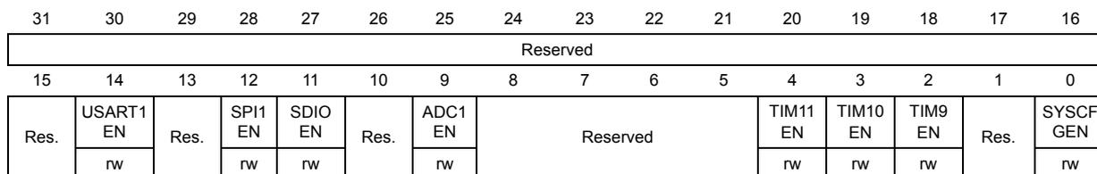
| 31 | 30 | 29 | 28 | 27 | 26 | 25 | 24 | 23 | 22 | 21 | 20 | 19 | 18 | 17 | 16 |
| Reserved | |||||||||||||||
| 15 | 14 | 13 | 12 | 11 | 10 | 9 | 8 | 7 | 6 | 5 | 4 | 3 | 2 | 1 | 0 |
| Res. | USART1 EN | Res. | SPI1 EN | SDIO EN | Res. | ADC1 EN | Reserved | TIM11 EN | TIM10 EN | TIM9 EN | Res. | SYSCF GEN | |||
| rw | rw | rw | rw | rw | rw | ||||||||||
Bits 31:15 Reserved, must be kept at reset value.
Bit 14 USART1EN : USART1 clock enable
This bit is set and cleared by software.
0: USART1 clock disabled
1: USART1 clock enabled
Bit 13 Reserved, must be kept at reset value.
Bit 12 SPI1EN : SPI 1 clock enable
This bit is set and cleared by software.
0: SPI 1 clock disabled
1: SPI 1 clock enabled
Bit 11 SDIOEN : SDIO clock enable
This bit is set and cleared by software.
0: SDIO clock disabled
1: SDIO clock enabled
Note: This bit is available in Cat.4 devices only.
Bit 10 Reserved, must be kept at reset value.
Bit 9 ADC1EN : ADC1 interface clock enable
This bit is set and cleared by software.
0: ADC1 interface disabled
1: ADC1 interface clock enabled
Bits 8:5 Reserved, must be kept at reset value.
Bit 4 TIM11EN : TIM11 timer clock enable
This bit is set and cleared by software.
0: TIM11 timer clock disabled
1: TIM11 timer clock enabled
Bit 3 TIM10EN : TIM10 timer clock enable
This bit is set and cleared by software.
0: TIM10 timer clock disabled
1: TIM10 timer clock enabled
Bit 2 TIM9EN : TIM9 timer clock enable
This bit is set and cleared by software.
0: TIM9 timer clock disabled
1: TIM9 timer clock enabled
Bit 1 Reserved, must be kept at reset value.
Bit 0 SYSCFGEN : System configuration controller clock enable
This bit is set and cleared by software.
0: System configuration controller clock disabled
1: System configuration controller clock enabled
6.3.10 APB1 peripheral clock enable register (RCC_APB1ENR)
Address: 0x24
Reset value: 0x0000 0000
Access: word, half-word and byte access
No wait state, except if the access occurs while an access to a peripheral on APB1 domain is on going. In this case, wait states are inserted until this access to APB1 peripheral is finished.
Note: When the peripheral clock is not active, the peripheral register values may not be readable by software and the returned value is always 0x0.
| 31 | 30 | 29 | 28 | 27 | 26 | 25 | 24 | 23 | 22 | 21 | 20 | 19 | 18 | 17 | 16 |
|---|---|---|---|---|---|---|---|---|---|---|---|---|---|---|---|
| COMP EN | Res. | DAC EN | PWR EN | Reserved | USB EN | I2C2 EN | I2C1 EN | UART5 EN | UART4 EN | USART3 EN | Res. | ||||
| rw | rw | rw | rw | rw | rw | rw | rw | rw | |||||||
| 15 | 14 | 13 | 12 | 11 | 10 | 9 | 8 | 7 | 6 | 5 | 4 | 3 | 2 | 1 | 0 |
|---|---|---|---|---|---|---|---|---|---|---|---|---|---|---|---|
| SPI3 EN | SPI2 EN | Reserved | WWD GEN | Res. | LCD EN | Reserved | TIM7 EN | TIM6 EN | TIM5 EN | TIM4 EN | TIM3 EN | TIM2 EN | |||
| rw | rw | rw | rw | rw | rw | rw | rw | rw | rw | ||||||
Bit 31 COMPEN : COMP interface clock enable
This bit is set and cleared by software.
0: COMP interface clock disabled
1: COMP interface clock enable
Bits 30 Reserved, must be kept at reset value.
Bit 29 DACEN : DAC interface clock enable
This bit is set and cleared by software.
0: DAC interface clock disabled
1: DAC interface clock enable
Bit 28 PWREN : Power interface clock enable
This bit is set and cleared by software.
0: Power interface clock disabled
1: Power interface clock enable
Bits 27:24 Reserved, must be kept at reset value.
Bit 23 USBEN : USB clock enable
This bit is set and cleared by software.
0: USB clock disabled
1: USB clock enabled
Bit 22 I2C2EN : I 2 C 2 clock enable
This bit is set and cleared by software.
0: I 2 C 2 clock disabled
1: I 2 C 2 clock enabled
Bit 21 I2C1EN : I 2 C 1 clock enable
This bit is set and cleared by software.
0: I 2 C 1 clock disabled
1: I 2 C 1 clock enabled
Bit 20 UART5EN : UART 5 clock enable
This bit is set and cleared by software.
0: UART 5 clock disabled
1: UART 5 clock enabled
Note: This bit is available in Cat.4, Cat.5 and Cat.6 devices only.
Bit 19 UART4EN : UART 4 clock enable
This bit is set and cleared by software.
Note: 0: UART 4 clock disabled
1: UART 4 clock enabled
This bit is available in Cat.4, Cat.5 and Cat.6 devices only.
Bit 18 USART3EN : USART 3 clock enable
This bit is set and cleared by software.
0: USART 3 clock disabled
1: USART 3 clock enabled
Bit 17 USART2EN : USART 2 clock enable
This bit is set and cleared by software.
0: USART 2 clock disabled
1: USART 2 clock enabled
Bit 16 Reserved, must be kept at reset value.
Bit 15 SPI3EN : SPI 3 clock enable
This bit is set and cleared by software.
0: SPI 3 clock disabled
1: SPI 3 clock enabled
Note: This bit is available in Cat.3, Cat.4, Cat.5 and Cat.6 devices only.
Bit 14 SPI2EN : SPI 2 clock enable
This bit is set and cleared by software.
0: SPI 2 clock disabled
1: SPI 2 clock enabled
Bits 13:12 Reserved, must be kept at reset value.
Bit 11 WWDGEN : Window watchdog clock enable
This bit is set and cleared by software.
0: Window watchdog clock disabled
1: Window watchdog clock enabled
Bit 10 Reserved, must be kept at reset value.
Bit 9 LCDEN : LCD clock enable
This bit is set and cleared by software.
0: LCD clock disabled
1: LCD clock enabled
Bits 8:6 Reserved, must be kept at reset value.
Bit 5 TIM7EN : Timer 7 clock enable
This bit is set and cleared by software.
0: Timer 7 clock disabled
1: Timer 7 clock enabled
Bit 4 TIM6EN : Timer 6 clock enable
This bit is set and cleared by software.
0: Timer 6 clock disabled
1: Timer 6 clock enabled
Bit 3 TIM5EN : Timer 5 clock enable
This bit is set and cleared by software.
0: Timer 5 clock disabled
1: Timer 5 clock enabled
Note: This bit is available in Cat.3, Cat.4, Cat.5 and Cat.6 devices only.
Bit 2 TIM4EN : Timer 4 clock enable
This bit is set and cleared by software.
0: Timer 4 clock disabled
1: Timer 4 clock enabled
Bit 1 TIM3EN : Timer 3 clock enable
This bit is set and cleared by software.
0: Timer 3 clock disabled
1: Timer 3 clock enabled
Bit 0 TIM2EN : Timer 2 clock enable
This bit is set and cleared by software.
0: Timer 2 clock disabled
1: Timer 2 clock enabled
6.3.11 AHB peripheral clock enable in low-power mode register (RCC_AHBLPENR)
Address offset: 0x28
Reset value: 0x0101 903F
Access: no wait state, word, half-word and byte access
Note: The peripheral clock is enabled in sleep mode only if it previously has been enabled in AHBENR register.
| 31 | 30 | 29 | 28 | 27 | 26 | 25 | 24 | 23 | 22 | 21 | 20 | 19 | 18 | 17 | 16 |
|---|---|---|---|---|---|---|---|---|---|---|---|---|---|---|---|
| Res. | FSMC LPEN | Reserved | AES LPEN | Res. | DMA2 LPEN | DMA1 LPEN | Reserved | SRAM LPEN | |||||||
| rw | rw | rw | rw | rw | |||||||||||
| 15 | 14 | 13 | 12 | 11 | 10 | 9 | 8 | 7 | 6 | 5 | 4 | 3 | 2 | 1 | 0 |
| FLITF LPEN | Reserved | CRC LPEN | Reserved | GPIOG LPEN | GPIOF LPEN | GPIOH LPEN | GPIOE LPEN | GPIOD LPEN | GPIOC LPEN | GPIOB LPEN | GPIOA LPEN | ||||
| rw | rw | rw | rw | rw | rw | rw | rw | rw | rw | ||||||
Bit 31 Reserved, must be kept at reset value.
Bit 30 FSMCLPEN : FSMC clock enable during Sleep mode
This bit is set and cleared by software.
0: FSMC clock disabled during Sleep mode
1: FSMC clock enabled during Sleep mode
Note: This bit is available in Cat.4 devices only.
Bits 29:28 Reserved, must be kept at reset value.
Bit 27 AESLPEN : AES clock enable during Sleep mode
This bit is set and cleared by software.
0: AES clock disabled during Sleep mode
1: AES clock enabled during Sleep mode
Note: This bit is available in STM32L16x devices only.
Bit 26 Reserved, must be kept at reset value.
Bit 25 DMA2LPEN : DMA2 clock enable during Sleep mode
This bit is set and cleared by software.
0: DMA2 clock disabled during Sleep mode
1: DMA2 clock enabled during Sleep mode
Note: This bit is available in Cat.3, Cat.4, Cat.5 and Cat.6 devices only.
Bit 24 DMA1LPEN : DMA1 clock enable during Sleep mode
This bit is set and cleared by software.
0: DMA1 clock disabled during Sleep mode
1: DMA1 clock enabled during Sleep mode
Bits 23:17 Reserved, must be kept at reset value.
Bit 16 SRAMLPEN : SRAM clock enable during Sleep mode
This bit is set and cleared by software.
0: SRAM clock disabled during Sleep mode
1: SRAM clock enabled during Sleep mode
Bit 15 FLITFLPEN : FLITF clock enable during Sleep mode
This bit can be written only when the Flash memory is in power down mode.
0: FLITF clock disabled during Sleep mode
1: FLITF clock enabled during Sleep mode
Bits 14:13 Reserved, must be kept at reset value.
Bit 12 CRCLPEN : CRC clock enable during Sleep mode
This bit is set and cleared by software.
0: CRC clock disabled during Sleep mode
1: CRC clock enabled during Sleep mode
Bits 11:8 Reserved, must be kept at reset value.
Bit 7 GPIOLPEN : IO port G clock enable during Sleep mode
This bit is set and cleared by software.
0: IO port G clock disabled during Sleep mode
1: IO port G clock enabled during Sleep mode
Note: This bit is available in Cat.4, Cat.5 and Cat.6 devices only.
Bit 6 GPIOFLPEN : IO port F clock enable during Sleep mode
This bit is set and cleared by software.
0: IO port F clock disabled during Sleep mode
1: IO port F clock enabled during Sleep mode
Note: This bit is available in Cat.4, Cat.5 and Cat.6 devices only.
Bit 5 GPIOHPEN : IO port H clock enable during Sleep mode
This bit is set and cleared by software.
0: IO port H clock disabled during Sleep mode
1: IO port H clock enabled during Sleep mode
- Bit 4
GPIOELPEN
: IO port E clock enable during Sleep mode
This bit is set and cleared by software.
0: IO port E clock disabled during Sleep mode
1: IO port E clock enabled during Sleep mode - Bit 3
GPIODLPEN
: IO port D clock enable during Sleep mode
This bit is set and cleared by software.
0: IO port D clock disabled during Sleep mode
1: IO port D clock enabled during Sleep mode - Bit 2
GPIOCLPEN
: IO port C clock enable during Sleep mode
This bit is set and cleared by software.
0: IO port C clock disabled during Sleep mode
1: IO port C clock enabled during Sleep mode - Bit 1
GPIOBLPEN
: IO port B clock enable during Sleep mode
This bit is set and cleared by software.
0: IO port B clock disabled during Sleep mode
1: IO port B clock enabled during Sleep mode - Bit 0
GPIOALPEN
: IO port A clock enable during Sleep mode
This bit is set and cleared by software.
0: IO port A clock disabled during Sleep mode
1: IO port A clock enabled during Sleep mode
6.3.12 APB2 peripheral clock enable in low-power mode register (RCC_APB2LPENR)
Address: 0x2C
Reset value: 0x0000 521D
Access: no wait states, word, half-word and byte access
Note: The peripheral clock is enabled in sleep mode only if it's previously has been enabled in APB2ENR register.
| 31 | 30 | 29 | 28 | 27 | 26 | 25 | 24 | 23 | 22 | 21 | 20 | 19 | 18 | 17 | 16 | |
|---|---|---|---|---|---|---|---|---|---|---|---|---|---|---|---|---|
| Reserved | ||||||||||||||||
| 15 | 14 | 13 | 12 | 11 | 10 | 9 | 8 | 7 | 6 | 5 | 4 | 3 | 2 | 1 | 0 | |
| Res. | USART1 LPEN | Res. | SPI1 LPEN | SDIO LPEN | Res. | ADC1 LPEN | Reserved | TIM11 LPEN | TIM10 LPEN | TIM9 LPEN | Res. | SYSCF GLPEN | ||||
| rw | rw | rw | rw | rw | rw | rw | rw | |||||||||
Bits 31:15 Reserved, must be kept at reset value.
- Bit 14
USART1LPEN
: USART1 clock enable during Sleep mode
This bit is set and cleared by software.
0: USART1 clock disabled during Sleep mode
1: USART1 clock enabled during Sleep mode
Bit 13 Reserved, must be kept at reset value.
Bit 12 SPI1LPEN : SPI 1 clock enable during Sleep mode
This bit is set and cleared by software.
0: SPI 1 clock disabled during Sleep mode
1: SPI 1 clock enabled during Sleep mode
Bit 11 SDIOLPEN : SDIO clock enable during Sleep mode
This bit is set and cleared by software.
0: SDIO clock disabled during Sleep mode
1: SDIO clock enabled during Sleep mode
Note: This bit is available in Cat.4 devices only.
Bit 10 Reserved, must be kept at reset value.
Bit 9 ADC1LPEN : ADC1 interface clock enable during Sleep mode
This bit is set and cleared by software.
0: ADC1 interface disabled during Sleep mode
1: ADC1 interface clock enabled during Sleep mode
Bits 8:5 Reserved, must be kept at reset value.
Bit 4 TIM11LPEN : TIM11 timer clock enable during Sleep mode
This bit is set and cleared by software.
0: TIM11 timer clock disabled during Sleep mode
1: TIM11 timer clock enabled during Sleep mode
Bit 3 TIM10LPEN : TIM10 timer clock enable during Sleep mode
This bit is set and cleared by software.
0: TIM10 timer clock disabled during Sleep mode
1: TIM10 timer clock enabled during Sleep mode
Bit 2 TIM9LPEN : TIM9 timer clock enable during Sleep mode
This bit is set and cleared by software.
0: TIM9 timer clock disabled during Sleep mode
1: TIM9 timer clock enabled during Sleep mode
Bit 1 Reserved, must be kept at reset value.
Bit 0 SYSCFGLPEN : System configuration controller clock enable during Sleep mode
This bit is set and cleared by software.
0: System configuration controller clock disabled during Sleep mode
1: System configuration controller clock enabled during Sleep mode
6.3.13 APB1 peripheral clock enable in low-power mode register (RCC_APB1LPENR)
Address: 0x30
Reset value: 0xB0E6 4A37
Access: no wait state, word, half-word and byte access
Note: The peripheral clock is enabled in sleep mode only if it's previously has been enabled in APB1ENR register.
| 31 | 30 | 29 | 28 | 27 | 26 | 25 | 24 | 23 | 22 | 21 | 20 | 19 | 18 | 17 | 16 |
|---|---|---|---|---|---|---|---|---|---|---|---|---|---|---|---|
| COMP LPEN | Res. | DAC LPEN | PWR LPEN | Reserved | USB LPEN | I2C2 LPEN | I2C1 LPEN | UART5 LPEN | UART4 LPEN | USART3 LPEN | USART2 LPEN | Res. | |||
| rw | rw | rw | rw | rw | rw | rw | rw | rw | rw | ||||||
| 15 | 14 | 13 | 12 | 11 | 10 | 9 | 8 | 7 | 6 | 5 | 4 | 3 | 2 | 1 | 0 |
| SPI3 LPEN | SPI2 LPEN | Reserved | WWD GLPE N | Res. | LCD LPEN | Reserved | TIM7 LPEN | TIM6 LPEN | TIM5 LPEN | TIM4 LPEN | TIM3 LPEN | TIM2 LPEN | |||
| rw | rw | rw | rw | rw | rw | rw | rw | rw | rw | ||||||
Bit 31 COMPLPEN : COMP interface clock enable during Sleep mode
This bit is set and cleared by software.
0: COMP interface clock disabled during Sleep mode
1: COMP interface clock enable during Sleep mode
Bit 30 Reserved, must be kept at reset value.
Bit 29 DACLPEN : DAC interface clock enable during Sleep mode
This bit is set and cleared by software.
0: DAC interface clock disabled during Sleep mode
1: DAC interface clock enable during Sleep mode
Bit 28 PWRLPEN : Power interface clock enable during Sleep mode
This bit is set and cleared by software.
0: Power interface clock disabled during Sleep mode
1: Power interface clock enable during Sleep mode
Bits 27:24 Reserved, must be kept at reset value.
Bit 23 USBLPEN : USB clock enable during Sleep mode
This bit is set and cleared by software.
0: USB clock disabled during Sleep mode
1: USB clock enabled during Sleep mode
Bit 22 I2C2LPEN : I 2 C 2 clock enable during Sleep mode
This bit is set and cleared by software.
0: I 2 C 2 clock disabled during Sleep mode
1: I 2 C 2 clock enabled during Sleep mode
Bit 21 I2C1LPEN : I 2 C 1 clock enable during Sleep mode
This bit is set and cleared by software.
0: I 2 C 1 clock disabled during Sleep mode
1: I 2 C 1 clock enabled during Sleep mode
Bit 20 UART5LPEN : USART 5 clock enable during Sleep mode
This bit is set and cleared by software.
0: USART 5 clock disabled during Sleep mode
1: USART 5 clock enabled during Sleep mode
Note: This bit is available in Cat.4, Cat.5 and Cat.6 devices only.
Bit 19 UART4LPEN : USART 4 clock enable during Sleep mode
This bit is set and cleared by software.
0: USART 4 clock disabled during Sleep mode
1: USART 4 clock enabled during Sleep mode
Note: This bit is available in Cat.4, Cat.5 and Cat.6 devices only.
Bit 18 USART3LPEN : USART 3 clock enable during Sleep mode
This bit is set and cleared by software.
0: USART 3 clock disabled during Sleep mode
1: USART 3 clock enabled during Sleep mode
Bit 17 USART2LPEN : USART 2 clock enable during Sleep mode
This bit is set and cleared by software.
0: USART 2 clock disabled during Sleep mode
1: USART 2 clock enabled during Sleep mode
Bit 16 Reserved, must be kept at reset value.
Bit 15 SPI3LPEN : SPI 3 clock enable during Sleep mode
This bit is set and cleared by software.
0: SPI 3 clock disabled during Sleep mode
1: SPI 3 clock enabled during Sleep mode
Note: This bit is available in Cat.3, Cat.4, Cat.5 and Cat.6 devices only.
Bit 14 SPI2LPEN : SPI 2 clock enable during Sleep mode
This bit is set and cleared by software.
0: SPI 2 clock disabled during Sleep mode
1: SPI 2 clock enabled during Sleep mode
Bits 13:12 Reserved, must be kept at reset value.
Bit 11 WWDGLPEN : Window watchdog clock enable during Sleep mode
This bit is set and cleared by software.
0: Window watchdog clock disabled during Sleep mode
1: Window watchdog clock enabled during Sleep mode
Bit 10 Reserved, must be kept at reset value.
Bit 9 LCDLPEN : LCD clock enable during Sleep mode
This bit is set and cleared by software.
0: LCD clock disabled during Sleep mode
1: LCD clock enabled during Sleep mode
Bits 8:6 Reserved, must be kept at reset value.
Bit 5 TIM7LPEN : Timer 7 clock enable during Sleep mode
This bit is set and cleared by software.
0: Timer 7 clock disabled during Sleep mode
1: Timer 7 clock enabled during Sleep mode
Bit 4 TIM6LPEN : Timer 6 clock enable during Sleep mode
This bit is set and cleared by software.
0: Timer 6 clock disabled during Sleep mode
1: Timer 6 clock enabled during Sleep mode
Bit 3 TIM5LPEN : Timer 5 clock enable during Sleep mode
This bit is set and cleared by software.
0: Timer 5 clock disabled during Sleep mode
1: Timer 5 clock enabled during Sleep mode
Note: This bit is available in Cat.3, Cat.4, Cat.5 and Cat.6 devices only.
Bit 2 TIM4LPEN : Timer 4 clock enable during Sleep mode
This bit is set and cleared by software.
0: Timer 4 clock disabled during Sleep mode
1: Timer 4 clock enabled during Sleep mode
Bit 1 TIM3LPEN : Timer 3 clock enable during Sleep mode
This bit is set and cleared by software.
0: Timer 3 clock disabled during Sleep mode
1: Timer 3 clock enabled during Sleep mode
Bit 0 TIM2LPEN : Timer 2 clock enable during Sleep mode
This bit is set and cleared by software.
0: Timer 2 clock disabled during Sleep mode
1: Timer 2 clock enabled during Sleep mode
6.3.14 Control/status register (RCC_CSR)
Address: 0x34
Power-on reset value: 0x0C00 0000,
Access: 0 ≤ wait state ≤ 3, word, half-word and byte access
Wait states are inserted in case of successive accesses to this register.
Note: The LSEON, LSEBYP, RTCSEL and RTCEN bits in the RCC control and status register (RCC_CSR) are in the RTC domain. As these bits are write protected after reset, the DBP bit in the Power control register (PWR_CR) has to be set to be able to modify them. Refer to Section RTC and RTC backup registers for further information. These bits are only reset after a RTC domain reset (see RTC and backup registers reset ). Any internal or external reset does not have any effect on them.
| 31 | 30 | 29 | 28 | 27 | 26 | 25 | 24 | 23 | 22 | 21 | 20 | 19 | 18 | 17 | 16 |
|---|---|---|---|---|---|---|---|---|---|---|---|---|---|---|---|
| LPWR RSTF | WWDG RSTF | IWDG RSTF | SFT RSTF | POR RSTF | PIN RSTF | OBLRS TF | RMVF | RTC RST | RTC EN | Reserved | RTCSEL[1:0] | ||||
| rw | rw | rw | rw | rw | rw | rw | rw | rw | rw | rw | |||||
| 15 | 14 | 13 | 12 | 11 | 10 | 9 | 8 | 7 | 6 | 5 | 4 | 3 | 2 | 1 | 0 |
| Reserved | LSECS SD | LSECS SON | LSE BYP | LSERDY | LSEON | Reserved | LSI RDY | LSION | |||||||
| r | rw | rw | r | rw | r | rw | |||||||||
This bit is set by hardware when a Low-power management reset occurs.
It is cleared by writing to the RMVF bit, or by a POR.
0: No Low-power management reset occurred
1: Low-power management reset occurred
For further information on Low-power management reset, refer to Low-power management reset .
Bit 30 WWDGRSTF: Window watchdog reset flagThis bit is set by hardware when a window watchdog reset occurs.
It is cleared by writing to the RMVF bit, or by a POR.
0: No window watchdog reset occurred
1: Window watchdog reset occurred
Bit 29 IWDGRSTF: Independent watchdog reset flagThis bit is set by hardware when an independent watchdog reset from V DD domain occurs.
It is cleared by writing to the RMVF bit, or by a POR.
0: No watchdog reset occurred
1: Watchdog reset occurred
Bit 28 SFTRSTF: Software reset flagThis bit is set by hardware when a software reset occurs.
It is cleared by writing to the RMVF bit, or by a POR.
0: No software reset occurred
1: Software reset occurred
Bit 27 PORRSTF: POR/PDR reset flagThis bit is set by hardware when a POR/PDR reset occurs.
It is cleared by writing to the RMVF bit.
0: No POR/PDR reset occurred
1: POR/PDR reset occurred
Bit 26 PINRSTF: PIN reset flagThis bit is set by hardware when a reset from the NRST pin occurs.
It is cleared by writing to the RMVF bit, or by a POR.
0: No reset from NRST pin occurred
1: Reset from NRST pin occurred
Bit 25 OBLRSTF Options bytes loading reset flagThis bit is set by hardware when an OBL reset occurs.
It is cleared by writing to the RMVF bit, or by a POR.
0: No OBL reset occurred
1: OBL reset occurred
Bit 24 RMVF: Remove reset flagThis bit is set by software to clear the reset flags.
0: No effect
1: Clear the reset flags
Bit 23 RTCRST: RTC software resetThis bit is set and cleared by software.
0: Reset not activated
1: Resets the RTC peripheral, its clock source selection and the backup registers.
Bit 22 RTCEN: RTC clock enableThis bit is set and cleared by software.
It is reset by setting the RTCRST bit or by a POR.
0: RTC clock disabled
1: RTC clock enabled
Bits 21:18 Reserved, must be kept at reset value.
Bits 17:16 RTCSEL[1:0]: RTC and LCD clock source selectionThese bits are set by software to select the clock source for the RTC.
Once the RTC and LCD clock source has been selected it cannot be switched until RTCRST is set or a Power On Reset occurred. The only exception is if the LSE oscillator clock was selected, if the LSE clock stops and it is detected by the CSS, in that case the clock can be switched.
00: No clock
01: LSE oscillator clock used as RTC/LCD clock
10: LSI oscillator clock used as RTC/LCD clock
11: HSE oscillator clock divided by a programmable prescaler (selection through the RTCPRE[1:0] bits in the RCC clock control register (RCC_CR)) used as the RTC/LCD clock
If the LSE or LSI is used as RTC clock source, the RTC continues to work in Stop and Standby low-power modes, and can be used as wake-up source. However, when the HSE clock is used as RTC clock source, the RTC cannot be used in Stop and Standby low-power modes.
Bits 15:13 Reserved, must be kept at reset value.
Bit 12 LSECSSD: CSS on LSE failure DetectionSet by hardware to indicate when a failure has been detected by the Clock Security System on the external 32 kHz oscillator (LSE).
Reset by power on reset and RTC software reset (RTCRST bit).
0: No failure detected on LSE (32 kHz oscillator)
1: Failure detected on LSE (32 kHz oscillator)
Note: This bit is available in Cat.2, Cat.3, Cat.4, Cat.5 and Cat.6 devices only.
Bit 11 LSECSSON CSS on LSE enableSet by software to enable the Clock Security System on LSE (32 kHz oscillator).
LSECSSON must be enabled after the LSE and LSI oscillators are enabled (LSEON and LSION bits enabled) and ready (LSERDY and LSIRDY flags set by hardware), and after the RTCSEL bit is selected.
Once enabled this bit cannot be disabled, except after an LSE failure detection (LSECSSD =1). In that case the software MUST disable the LSECSSON bit.
Reset by power on reset and RTC software reset (RTCRST bit).
0: CSS on LSE (32 kHz oscillator) OFF
1: CSS on LSE (32 kHz oscillator) ON
Note: This bit is available in Cat.2, Cat.3, Cat.4, Cat.5 and Cat.6 devices only.
Bit 10 LSEBYP: External low-speed oscillator bypassThis bit is set and cleared by software to bypass oscillator in debug mode. This bit can be written only when the LSE oscillator is disabled.
It is reset by setting the RTCRST bit or by a POR.
0: LSE oscillator not bypassed
1: LSE oscillator bypassed
Bit 9 LSERDY : External low-speed oscillator ready
This bit is set and cleared by hardware to indicate when the LSE oscillator is stable. After the LSEON bit is cleared, LSERDY goes low after 6 LSE oscillator clock cycles.
It is reset by setting the RTCRST bit or by a POR.
0: External 32 kHz oscillator not ready
1: External 32 kHz oscillator ready
Bit 8 LSEON : External low-speed oscillator enable
This bit is set and cleared by software.
It is reset by setting the RTCRST bit or by a POR.
0: LSE oscillator OFF
1: LSE oscillator ON
Bits 7:2 Reserved, must be kept at reset value.
Bit 1 LSIRDY : Internal low-speed oscillator ready
This bit is set and cleared by hardware to indicate when the LSI oscillator is stable. After the LSION bit is cleared, LSIRDY goes low after 3 LSI oscillator clock cycles. This bit is kept set if IWDG is activated.
This bit is reset by system reset.
0: LSI oscillator not ready
1: LSI oscillator ready
Bit 0 LSION : Internal low-speed oscillator enable
This bit is set and cleared by software.
It is reset by system reset.
0: LSI oscillator OFF
1: LSI oscillator ON
6.3.15 RCC register map
The following table gives the RCC register map and the reset values. The reserved memory areas are highlighted in gray in the table.
Table 36. RCC register map and reset values
| Off-set | Register | 31 | 30 | 29 | 28 | 27 | 26 | 25 | 24 | 23 | 22 | 21 | 20 | 19 | 18 | 17 | 16 | 15 | 14 | 13 | 12 | 11 | 10 | 9 | 8 | 7 | 6 | 5 | 4 | 3 | 2 | 1 | 0 | |
|---|---|---|---|---|---|---|---|---|---|---|---|---|---|---|---|---|---|---|---|---|---|---|---|---|---|---|---|---|---|---|---|---|---|---|
| 0x00 | RCC_CR | Reserved | RTCPRE1 | RTCPRE0 | CSSON | Reserved | PLL RDY | PLL ON | Reserved | HSEBYP | HSERDY | HSEON | Reserved | MSIRDY | MSION | Reserved | HSIRDY | HSION | ||||||||||||||||
| Reset value | 0 | 0 | 0 | 0 | 0 | x | 0 | 0 | 1 | 1 | 0 | 0 | ||||||||||||||||||||||
| 0x04 | RCC_ICSCR | MSITRIM[7:0] | MSICAL[7:0] | MSIRANGE[2:0] | HSITRIM[4:0] | HSICAL[7:0] | ||||||||||||||||||||||||||||
| Reset value | 0 | 0 | 0 | 0 | 0 | 0 | 0 | 0 | x | x | x | x | x | x | x | x | 1 | 0 | 1 | 1 | 0 | 0 | 0 | 0 | x | x | x | x | x | x | x | x | ||
| 0x08 | RCC_CFGR | Reserved | MCOPRE [2:0] | Reserved | MCOSEL [2:0] | PLL DIV [1:0] | PLLMUL[3:0] | Reserved | PLLSRC | Reserved | PPRE2 [2:0] | PPRE1 [2:0] | HPRE[3:0] | SWS [1:0] | SW [1:0] | |||||||||||||||||||
| Reset value | 0 | 0 | 0 | 0 | 0 | 0 | 0 | 0 | 0 | 0 | 0 | 0 | 0 | 0 | 0 | 0 | 0 | 0 | 0 | 0 | 0 | 0 | 0 | 0 | 0 | 0 | 0 | |||||||
| Off-set | Register | 31 | 30 | 29 | 28 | 27 | 26 | 25 | 24 | 23 | 22 | 21 | 20 | 19 | 18 | 17 | 16 | 15 | 14 | 13 | 12 | 11 | 10 | 9 | 8 | 7 | 6 | 5 | 4 | 3 | 2 | 1 | 0 | |
|---|---|---|---|---|---|---|---|---|---|---|---|---|---|---|---|---|---|---|---|---|---|---|---|---|---|---|---|---|---|---|---|---|---|---|
| 0x0C | RCC_CIR | Reserved | CSSC | LSECSSC | MSIRDYC | PLLRDYC | HSERDYC | HSIRDYC | LSERDYC | LSIRDYC | Reserved | LSECSSIE | MSIRDYIE | PLLRDYIE | HSERDYIE | HSIRDYIE | LSERDYIE | LSIRDYIE | CSSF | Reserved | MSIRDYF | PLLRDYF | HSERDYF | HSIRDYF | LSERDYF | LSIRDYF | ||||||||
| Reset value | 0 | 0 | 0 | 0 | 0 | 0 | 0 | 0 | 0 | 0 | 0 | 0 | 0 | 0 | 0 | 0 | 0 | 0 | 0 | 0 | 0 | 0 | ||||||||||||
| 0x10 | RCC_AHBRSTR | Reserved | FSMCRST | Reserved | AESRST | Reserved | DMA2RST | DMA1RST | Reserved | FLITFRST | Reserved | Reserved | CRCRST | Reserved | GPIOGRST | GPIOFRST | GPIOHRST | GPIOERST | GPIODRST | GPIOCRST | GPIOBRST | GPIOARST | ||||||||||||
| Reset value | 0 | 0 | 0 | 0 | 0 | 0 | 0 | 0 | 0 | 0 | 0 | 0 | 0 | 0 | ||||||||||||||||||||
| 0x14 | RCC_APB2RSTR | Reserved | USART1RST | Reserved | SPI1RST | SDIORST | Reserved | ADC1RST | Reserved | TIM11RST | TIM10RST | TIM9RST | Reserved | SYSCFGRST | ||||||||||||||||||||
| Reset value | 0 | 0 | 0 | 0 | 0 | 0 | 0 | 0 | ||||||||||||||||||||||||||
| 0x18 | RCC_APB1RSTR | COMPRST | Reserved | DACRST | PWRRST | Reserved | USBRST | I2C2RST | I2C1RST | UART5RST | UART4RST | USART3RST | USART2RST | Reserved | SPI3RST | SPI2RST | Reserved | WWDGRST | Reserved | LCDRST | Reserved | TIM7RST | TIM6RST | TIM5RST | TIM4RST | TIM3RST | TIM2RST | |||||||
| Reset value | 0 | 0 | 0 | 0 | 0 | 0 | 0 | 0 | 0 | 0 | 0 | 0 | 0 | 0 | 0 | 0 | 0 | 0 | 0 | 0 | ||||||||||||||
| 0x1C | RCC_AHBENR | Reserved | FSMCEN | Reserved | AESEN | Reserved | DMA2EN | DMA1EN | Reserved | FLITFEN | Reserved | Reserved | CRCEN | Reserved | GPIOPGEN | GPIOPFEN | GPIOPHEN | GPIOEPEN | GPIODPEN | GPIOCPEN | GPIOBPEN | GPIOPAEN | ||||||||||||
| Reset value | 0 | 0 | 0 | 0 | 1 | 0 | 0 | 0 | 0 | 0 | 0 | 0 | 0 | 0 | ||||||||||||||||||||
| 0x20 | RCC_APB2ENR | Reserved | USART1EN | Reserved | SPI1EN | SDIOEN | Reserved | ADC1EN | Reserved | TIM11EN | TIM10EN | TIM9EN | Reserved | SYSCFGEN | ||||||||||||||||||||
| Reset value | 0 | 0 | 0 | 0 | 0 | 0 | 0 | 0 | ||||||||||||||||||||||||||
| 0x24 | RCC_APB1ENR | COMPEN | Reserved | DACEN | PWREN | Reserved | USBEN | I2C2EN | I2C1EN | UART5EN | UART4EN | USART3EN | USART2EN | Reserved | SPI3EN | SPI2EN | Reserved | WWDGEN | Reserved | LCDEN | Res. | TIM7EN | TIM6EN | TIM5EN | TIM4EN | TIM3EN | TIM2EN | |||||||
| Reset value | 0 | 0 | 0 | 0 | 0 | 0 | 0 | 0 | 0 | 0 | 0 | 0 | 0 | 0 | 0 | 0 | 0 | 0 | 0 | 0 | ||||||||||||||
| 0x28 | RCC_AHBLPENR | Reserved | FSMCLPEN | Reserved | AESLPEN | Reserved | DMA2LPEN | DMA1LPEN | Reserved | SRAMLPEN | FLITFLPEN | Reserved | Reserved | CRCLPEN | Reserved | GPIOGLPEN | GPIOFLPEN | GPIOHLPEN | GPIOELPEN | GPIODLPEN | GPIOCLPEN | GPIOBLPEN | GPIOALPEN | |||||||||||
| Reset value | 1 | 1 | 1 | 1 | 1 | 1 | 1 | 1 | 1 | 1 | 1 | 1 | 1 | 1 | 1 | |||||||||||||||||||
Table 36. RCC register map and reset values (continued)
| Off-set | Register | 31 | 30 | 29 | 28 | 27 | 26 | 25 | 24 | 23 | 22 | 21 | 20 | 19 | 18 | 17 | 16 | 15 | 14 | 13 | 12 | 11 | 10 | 9 | 8 | 7 | 6 | 5 | 4 | 3 | 2 | 1 | 0 | |
|---|---|---|---|---|---|---|---|---|---|---|---|---|---|---|---|---|---|---|---|---|---|---|---|---|---|---|---|---|---|---|---|---|---|---|
| 0x2C | RCC_APB2L P ENR | Reserved | USART1LPEN | Reserved | SPI1LPEN | SDIOLPEN | Reserved | ADC1LPEN | Reserved | TIM11LPEN | TIM10LPEN | TIM9LPEN | Reserved | SYSCFGLPEN | ||||||||||||||||||||
| Reset value | 1 | 1 | 1 | 1 | 1 | 1 | 1 | 1 | ||||||||||||||||||||||||||
| 0x30 | RCC_APB1L P ENR | COMPLPEN | Reserved | DACLPEN | PWRLPEN | Reserved | USBLPEN | I2C2LPEN | I2C1LPEN | USART5LPEN | USART4LPEN | USART3LPEN | USART2LPEN | Reserved | SPI3LPEN | SPI2LPEN | Reserved | WWDGLPEN | Reserved | LCDLPEN | Res. | TIM7LPEN | TIM6LPEN | TIM5LPEN | TIM4LPEN | TIM3LPEN | TIM2LPEN | |||||||
| Reset value | 1 | 1 | 1 | 1 | 1 | 1 | 1 | 1 | 1 | 1 | 1 | 1 | 1 | 1 | 1 | 1 | 1 | 1 | 1 | 1 | ||||||||||||||
| 0x03 4 | RCC_CSR | LPWRSTF | WWDGRSTF | IWDGRSTF | SFTRSTF | PORRSTF | PINRSTF | OBLRSTF | RMVF | RTCRST | RTCEN | Reserved | RTC SEL [1:0] | Reserved | LSECSSD | LSECSSON | LSEBYP | LSERDY | LSEON | Reserved | LSIRDY | LSION | ||||||||||||
| Reset value | 0 | 0 | 0 | 0 | 1 | 1 | 0 | 0 | 0 | 0 | 0 | 0 | 0 | 0 | 0 | 0 | 0 | 0 | 0 | |||||||||||||||
Refer to Table 5 on page 47 for the register boundary addresses.