5. Power control (PWR)
5.1 Power supplies
The device requires a 1.8-to-3.6 V \( V_{DD} \) operating voltage supply (down to 1.65 V at power down) when the BOR is available. The device requires a 1.65-to-3.6 V \( V_{DD} \) operating voltage supply when the BOR is not available.
An embedded linear voltage regulator is used to supply the internal digital power, ranging from 1.2 to 1.8 V.
- • \( V_{DD} = 1.8 \) V (at power on) or 1.65 V (at power down) to 3.6 V when the BOR is available. \( V_{DD} = 1.65 \) V to 3.6 V, when BOR is not available
\( V_{DD} \) is the external power supply for I/Os and internal regulator. It is provided externally through \( V_{DD} \) pins.
- • \( V_{CORE} = 1.2 \) to 1.8 V
\( V_{CORE} \) is the power supply for digital peripherals, SRAM and Flash memory. It is generated by a internal voltage regulator. Three \( V_{CORE} \) ranges can be selected by software depending on \( V_{DD} \) (refer Figure 9 ).
- • \( V_{SSA} \) , \( V_{DDA} = 1.8 \) V (at power on) or 1.65 V (at power down) to 3.6 V, when BOR is available and \( V_{SSA} \) , \( V_{DDA} = 1.65 \) to 3.6 V, when BOR is not available.
\( V_{DDA} \) is the external analog power supply for ADC, DAC, reset blocks, RC oscillators and PLL. The minimum voltage to be applied to \( V_{DDA} \) is 1.8 V when the ADC is used.
- • \( V_{REF-} \) , \( V_{REF+} \)
\( V_{REF+} \) is the input reference voltage.
\( V_{REF-} \) and \( V_{REF+} \) are only available as external pins on LQFP144, UFBGA132, LQFP100, UFBGA100, and TFBGA64 packages, otherwise they are bonded to \( V_{SSA} \) and \( V_{DDA} \) , respectively.
- • \( V_{LCD} = 2.5 \) to 3.6 V
The LCD controller can be powered either externally through \( V_{LCD} \) pin, or internally from an internal voltage generated by the embedded step-up converter.
Figure 8. Power supply overview
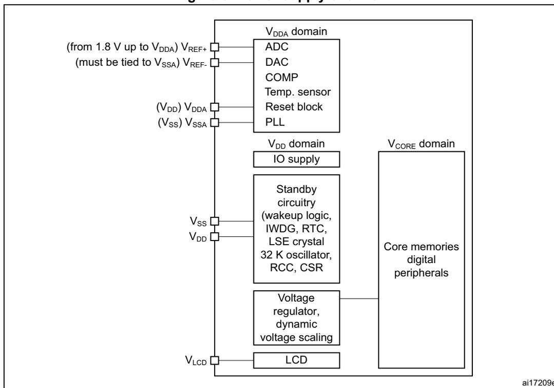
- 1. \( V_{DDA} \) and \( V_{SSA} \) must be connected to \( V_{DD} \) and \( V_{SS} \) , respectively.
- 2. When available (depending on packages), \( V_{REF-} \) must be tied to \( V_{SSA} \) .
- 3. Depending on the operating power supply range used, some peripherals may be used with limited functionalities or performance. For more details, refer to section "General operating conditions" in STM32L1xxxx datasheets.
5.1.1 Independent A/D and DAC converter supply and reference voltage
To improve conversion accuracy, the ADC and the DAC have an independent power supply that can be filtered separately, and shielded from noise on the PCB.
- • The ADC voltage supply input is available on a separate \( V_{DDA} \) pin
- • An isolated supply ground connection is provided on the \( V_{SSA} \) pin
On BGA 64-pin and all packages with 100 pins or more
To ensure a better accuracy on low-voltage inputs and outputs, the user can connect to \( V_{REF+} \) a separate external reference voltage lower than \( V_{DD} \) . \( V_{REF+} \) is the highest voltage, represented by the full scale value, for an analog input (ADC) or output (DAC) signal.
- • For ADC
- – \( 2.4 \text{ V} \leq V_{REF+} = V_{DDA} \) for full speed (ADCCLK = 16 MHz, 1 Msps)
- – \( 1.8 \text{ V} \leq V_{REF+} = V_{DDA} \) for medium speed (ADCCLK = 8 MHz, 500 Ksps)
- – \( 2.4 \text{ V} \leq V_{REF+} \neq V_{DDA} \) for medium speed (ADCCLK = 8 MHz, 500 Ksps)
- – \( 1.8 \text{ V} \leq V_{REF+} < V_{DDA} \) for low speed (ADCCLK = 4 MHz, 250 Ksps)
- – When Product voltage range 3 is selected ( \( V_{Core} = 1.2 \text{ V} \) ) the ADC is low speed (ADCCLK = 4 MHz, 250 Ksps)
- • For DAC
- – \( 1.8 \text{ V} \leq V_{REF+} < V_{DDA} \)
- • When \( V_{DDA} \) is higher than 2.4 V, the voltage on \( V_{REF+} \) may range from 2.4 V to \( V_{DDA} \) .
- • When \( V_{DDA} \) is below 2.4 V, \( V_{REF+} \) must be equal to \( V_{DDA} \) .
On packages with 64 pins or less (except BGA package)
\( V_{REF+} \) and \( V_{REF-} \) pins are not available. They are internally connected to the ADC voltage supply ( \( V_{DDA} \) ) and ground ( \( V_{SSA} \) ).
5.1.2 Independent LCD supply
The \( V_{LCD} \) pin is provided to control the contrast of the glass LCD. This pin can be used in two ways:
- • It can receive from an external circuitry the desired maximum voltage that is provided on segment and common lines to the glass LCD by the microcontroller.
- • It can also be used to connect an external capacitor that is used by the microcontroller for its voltage step-up converter. This step-up converter is controlled by software to provide the desired voltage to segment and common lines of the glass LCD.
The voltage provided to segment and common lines defines the contrast of the glass LCD pixels. This contrast can be reduced when you configure the dead time between frames.
- • When an external power supply is provided to the \( V_{LCD} \) pin, it should range from 2.5 V to 3.6 V. It does not depend on \( V_{DD} \) .
- • When the LCD is based on the internal step-up converter, the \( V_{LCD} \) pin should be connected to a capacitor (see the product datasheets for further information).
5.1.3 RTC and RTC backup registers
The real-time clock (RTC) is an independent BCD timer/counter. The RTC provides a time-of-day clock/calendar, two programmable alarm interrupts, and a periodic programmable wakeup flag with interrupt capability. The RTC contains 20 backup data registers (80 bytes) in Cat.1 and Cat.2 devices, 32 backup data registers (128 bytes) in Cat.3, Cat.4, Cat.5 and Cat.6 devices and 5 backup data registers (20 bytes) for value line devices. These backup registers are reset when a tamper detection event occurs. For more details refer to Real-time clock (RTC) section.
RTC registers access
After reset, the RTC Registers (RTC registers and RTC backup registers) are protected against possible stray write accesses. To enable access to the RTC Registers, proceed as follows:
- 1. Enable the power interface clock by setting the PWREN bits in the RCC_APB1ENR register.
- 2. Set the DBP bit in the PWR_CR register (see Section 5.4.1 ).
- 3. Select the RTC clock source through RTCSEL[1:0] bits in RCC_CSR register.
- 4. Enable the RTC clock by programming the RTCEN bit in the RCC_CSR register.
5.1.4 Voltage regulator
An embedded linear voltage regulator supplies all the digital circuitries except for the Standby circuitry. The regulator output voltage ( \( V_{CORE} \) ) can be programmed by software to three different ranges within 1.2 - 1.8 V (typical) (see Section 5.1.5 ).
The voltage regulator is always enabled after Reset. It works in three different modes: main (MR), low-power (LPR) and power down, depending on the application modes.
- • In Run mode, the regulator is main (MR) mode and supplies full power to the \( V_{CORE} \) domain (core, memories and digital peripherals).
- • In Low-power run mode, the regulator is in low-power (LPR) mode and supplies low-power to the \( V_{CORE} \) domain, preserving the contents of the registers and internal SRAM.
- • In Sleep mode, the regulator is main (MR) mode and supplies full power to the \( V_{CORE} \) domain, preserving the contents of the registers and internal SRAM.
- • In low-power sleep mode, the regulator is in low-power (LPR) mode and supplies low-power to the \( V_{CORE} \) domain, preserving the contents of the registers and internal SRAM.
- • In Stop mode the regulator supplies low-power to the \( V_{CORE} \) domain, preserving the content of registers and internal SRAM.
- • In Standby mode, the regulator is powered off. The content of the registers and SRAM are lost except for the Standby circuitry.
5.1.5 Dynamic voltage scaling management
The dynamic voltage scaling is a power management technique which consists in increasing or decreasing the voltage used for the digital peripherals ( \( V_{CORE} \) ), according to the circumstances.
Dynamic voltage scaling to increase \( V_{CORE} \) is known as overvolting. It can be used to improve the device performance. Refer to Figure 9 for a description of the STM32L1xxxx operating conditions versus performance.
Dynamic voltage scaling to decrease \( V_{CORE} \) is known as undervolting. It is performed to save power, particularly in laptops and other mobile devices where the energy comes from a battery and is thus limited.
Range 1
Range 1 is the “high performance” range.
The voltage regulator outputs a 1.8 V voltage (typical) as long as the \( V_{DD} \) input voltage is in the range 1.71 V 3.6 V (a) . Flash program and erase operations can be performed in this range.
Range 2 and 3
The regulator can also be programmed to output a regulated 1.5 V (typical, range 2) or a 1.2 V (typical, range 3) without any limitations on \( V_{DD} \) (1.65 to 3.6 V).
- • At 1.5 V, the Flash memory is still functional but with medium read access time. This is the “medium performance” range. Program and erase operations on the Flash memory are still possible.
- • At 1.2 V, the Flash memory is still functional but with slow read access time. This is the “low performance” range. Program and erase operations on the Flash memory are not possible under these conditions.
Refer to Table 26 for details on the performance for each range.
Table 26. Performance versus \( V_{CORE} \) ranges
| CPU performance | Power performance | \( V_{CORE} \) range | Typical Value (V) | Max frequency (MHz) | \( V_{DD} \) range | |
|---|---|---|---|---|---|---|
| 1 WS | 0 WS | |||||
| High | Low | 1 | 1.8 | 32 | 16 | 1.71 - 3.6 (1) |
| Medium | Medium | 2 | 1.5 | 16 | 8 | 1.65 - 3.6 |
| Low | High | 3 | 1.2 | 4.2 | 2.1 | |
1. Depending on the device, \( V_{DD} \) range 1 is either 1.71 to 3.6V or 2.0V to 3.6V. Refer to the specific product datasheet.
a. Depending on the device, \( V_{DD} \) range 1 is either 1.71 to 3.6V or 2.0V to 3.6V. Refer to the specific product datasheet.
Figure 9. STM32L1xxxx performance versus\( V_{DD} \) and \( V_{CORE} \) range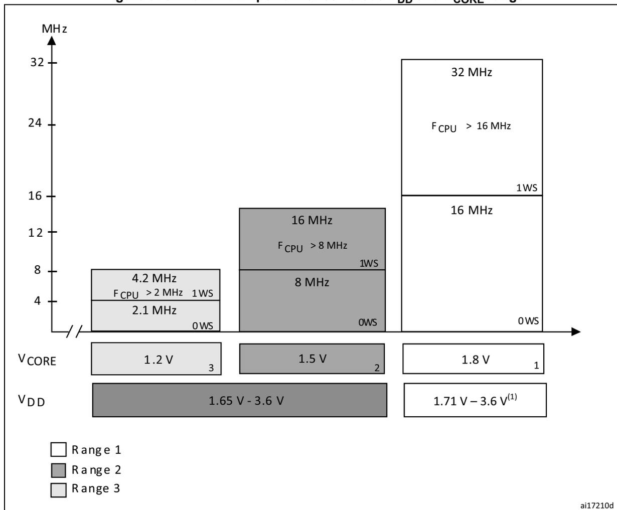
| Range | \( V_{CORE} \) (V) | \( V_{DD} \) (V) | Max Frequency (MHz) | Wait States (WS) | Condition |
|---|---|---|---|---|---|
| Range 1 | 1.8 | 1.71 – 3.6 (1) | 32 | 1WS | \( F_{CPU} > 16 \) MHz |
| Range 1 | 1.8 | 1.71 – 3.6 (1) | 16 | 0WS | |
| Range 2 | 1.5 | 1.65 – 3.6 | 16 | 1WS | \( F_{CPU} > 8 \) MHz |
| Range 2 | 1.5 | 1.65 – 3.6 | 8 | 0WS | |
| Range 3 | 1.2 | 1.65 – 3.6 | 4.2 | 1WS | \( F_{CPU} > 2 \) MHz |
| Range 3 | 1.2 | 1.65 – 3.6 | 2.1 | 0WS |
ai17210d
1. Depending on the device, \( V_{DD} \) range 1 is either 1.71 to 3.6V or 2.0V to 3.6V. Refer to the specific product datasheet.
5.1.6 Dynamic voltage scaling configuration
The following sequence is required to program the voltage regulator ranges:
- 1. Check \( V_{DD} \) to identify which ranges are allowed (see Figure 9: STM32L1xxxx performance versus \( V_{DD} \) and \( V_{CORE} \) range ).
- 2. Poll VOSF bit of in PWR_CSR. Wait until it is reset to 0.
- 3. Configure the voltage scaling range by setting the VOS[12:11] bits in the PWR_CR register.
- 4. Poll VOSF bit of in PWR_CSR register. Wait until it is reset to 0.
Note: During voltage scaling configuration, the system clock is stopped until the regulator is stabilized (VOSF=0). This must be taken into account during application development, in case a critical reaction time to interrupt is needed, and depending on peripheral used (timer, communication,...).
5.1.7 Voltage regulator and clock management when \( V_{DD} \) drops below 2.0 V
When \( V_{CORE} \) range 1 is selected and \( V_{DD} \) drops below 2.0 V, the application must reconfigure the system.
A three-step sequence is required to reconfigure the system:
- 1. Detect that
\(
V_{DD}
\)
drops below 2.0 V:
Use the PVD to monitor the \( V_{DD} \) voltage and to generate an interrupt when the voltage goes under the selected level. To detect the 2.0 V voltage limit, the application can select by software PVD threshold 2 (2.26 V typical). For more details on the PVD, refer to Section 5.2.3 . - 2. Adapt the clock frequency to the voltage range that is selected at next step:
Below 2.0 V, the system clock frequency is limited to 16 MHz for range 2 and 4.2 MHz for range 3. - 3. Select the required voltage range:
Note that when \( V_{DD} \) is below 1.71 V, only range 2 or range 3 can be selected.
Note: When \( V_{CORE} \) range 2 or range 3 is selected and \( V_{DD} \) drops below 2.0 V, no system reconfiguration is required.
5.1.8 Voltage regulator and clock management when modifying the \( V_{CORE} \) range
When \( V_{DD} \) is above 2.0 V, any of the 3 voltage ranges can be selected:
- • When the voltage range is above the targeted voltage range (e.g. from range 1 to 2):
- a) Adapt the clock frequency to the lower voltage range that is selected at next step.
- b) Select the required voltage range.
- • When the voltage range is below the targeted voltage range (e.g. from range 3 to 1):
- a) Select the required voltage range.
- b) Tune the clock frequency if needed.
When \( V_{DD} \) is below 2.0 V, only range 2 and 3 can be selected:
- • From range 2 to range 3
- a) Adapt the clock frequency to voltage range 3.
- b) Select voltage range 3.
- • From range 3 to range 2
- a) Select the voltage range 2.
- b) Tune the clock frequency if needed.
5.2 Power supply supervisor
The device has an integrated zeropower power on reset (POR)/power down reset (PDR), coupled with a brown out reset (BOR) circuitry. For devices operating between 1.8 and 3.6 V, the BOR is always active at power-on and ensures proper operation starting from 1.8 V. After the 1.8 V BOR threshold is reached, the option byte loading process starts, either to confirm or modify default thresholds, or to disable BOR permanently (in which case, the \( V_{DD} \) min value at power down is 1.65 V). For devices operating between 1.65 V and 3.6 V, the
BOR is permanently disabled. Consequently, the start-up time at power-on can be decreased down to 1 ms typically.
Five BOR thresholds can be configured by option bytes, starting from 1.65 to 3 V. To reduce the power consumption in Stop mode, the internal voltage reference, \( V_{REFINT} \) , can be automatically switch off. The device remains in reset mode when \( V_{DD} \) is below a specified threshold, \( V_{POR} \) , \( V_{PDR} \) or \( V_{BOR} \) , without the need for any external reset circuit.
The device features an embedded programmable voltage detector (PVD) that monitors the \( V_{DD}/V_{DDA} \) power supply and compares it to the \( V_{PVD} \) threshold. 7 different PVD levels can be selected by software between 1.85 and 3.05 V, with a 200 mV step. An interrupt can be generated when \( V_{DD}/V_{DDA} \) drops below the \( V_{PVD} \) threshold and/or when \( V_{DD}/V_{DDA} \) is higher than the \( V_{PVD} \) threshold. The interrupt service routine then generates a warning message and/or put the MCU into a safe state. The PVD is enabled by software.
The different power supply supervisor (POR, PDR, BOR, PVD) are illustrated in Figure 10 .
Figure 10. Power supply supervisors
- 1. The PVD is available on all STM32L devices and it is enabled or disabled by software.
- 2. The BOR is available only on devices operating from 1.8 to 3.6 V, and unless disabled by option byte it
masks the POR/PDR threshold.
- 3. When the BOR is disabled by option byte, the reset is asserted when \( V_{DD} \) goes below PDR level
- 4. For devices operating from 1.65 to 3.6 V, there is no BOR and the reset is released when \( V_{DD} \) goes above POR level and asserted when \( V_{DD} \) goes below PDR level
5.2.1 Power on reset (POR)/power down reset (PDR)
The device has an integrated POR/PDR circuitry that allows operation down to 1.5 V.
During power on, the device remains in Reset mode when \( V_{DD}/V_{DDA} \) is below a specified threshold, \( V_{POR} \) , without the need for an external reset circuit. The POR feature is always enabled and the POR threshold is 1.5 V.
During power down, the PDR keeps the device under reset when the supply voltage ( \( V_{DD} \) ) drops below the \( V_{PDR} \) threshold. The PDR feature is always enabled and the PDR threshold is 1.5 V.
The POR and PDR are used only when the BOR is disabled (see Section 5.2.2: Brown out reset ). To insure the minimum operating voltage (1.65 V), the BOR should be configured to BOR Level 0. When the BOR is disabled, a “grey zone” exist between the minimum operating voltage (1.65 V) and the \( V_{POR}/V_{PDR} \) threshold. This means that \( V_{DD} \) can be lower than 1.65 V without device reset until the \( V_{PDR} \) threshold is reached.
For more details concerning the power on/power down reset threshold, refer to the electrical characteristics of the datasheet.
Figure 11. Power on reset/power down reset waveform
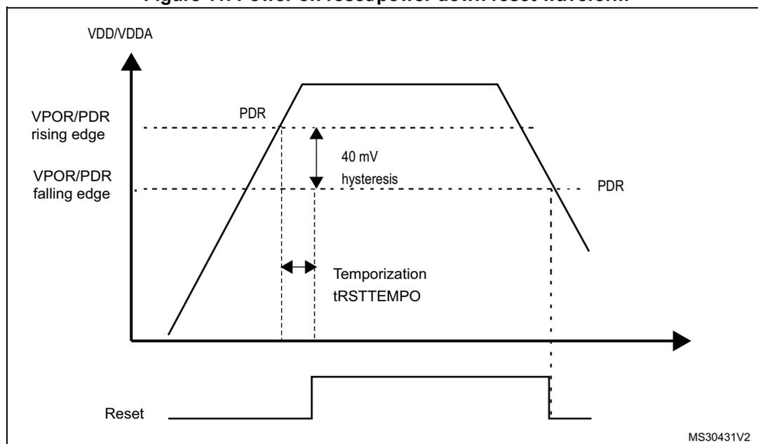
The figure is a timing diagram showing the relationship between the supply voltage ( \( V_{DD}/V_{DDA} \) ) and the Reset signal. The top graph shows \( V_{DD}/V_{DDA} \) rising from 0V to a maximum value and then falling. The Reset signal is shown below it. The Reset signal is initially low (active). As \( V_{DD}/V_{DDA} \) rises, the Reset signal goes high (inactive) after a delay labeled as Temporization \( t_{RSTTEMPO} \) once the voltage reaches the \( V_{POR}/V_{PDR} \) rising edge threshold. As \( V_{DD}/V_{DDA} \) falls, the Reset signal goes low (active) when the voltage reaches the \( V_{POR}/V_{PDR} \) falling edge threshold. The difference between the rising and falling thresholds is labeled as 40 mV hysteresis. The PDR threshold is indicated on the falling edge of the \( V_{DD}/V_{DDA} \) signal.
5.2.2 Brown out reset
The device exists in two versions:
- • The version with BOR activated at power-on operates between 1.8 V and 3.6 V.
- • The other version without BOR operates between 1.65 V and 3.6 V.
After the \( V_{DD} \) threshold is reached (1.65 V or 1.8 V depending on the BOR which is active or not at power-on), the option byte loading process starts, either to confirm or to modify default thresholds, or to disable the BOR permanently: in this case, the \( V_{DD} \) min value becomes 1.65 V (whatever the version, BOR active or not, at power-on).
When BOR is active at power-on, it ensures a proper operation starting from 1.8 V whatever the power ramp-up phase before it reaches 1.8 V.
When BOR is not active at power-up, the power ramp-up should guarantee that 1.65 V is reached on \( V_{DD} \) at least 1 ms after it exits the POR area. As the POR/PDR thresholds are at 1.5 V, a "grey zone" exists between the \( V_{POR}/V_{PDR} \) thresholds and the minimum product operating voltage 1.65 V.
Five BOR thresholds are available through option bytes, starting from 1.8 V to 3 V. To reduce the power consumption in Stop mode, it is possible to automatically switch off the internal reference voltage ( \( V_{REFINT} \) ) in Stop mode. The device remains in reset mode when \( V_{DD} \) is below a specified threshold, \( V_{POR}/V_{PDR} \) or \( V_{BOR} \) , without the need for any external reset circuit.
The five programmable \( V_{BOR} \) thresholds are:
- • BOR Level 1 ( \( V_{BOR1} \) ): reset threshold level for 1.69 to 1.80 V voltage range
- • BOR Level 2 ( \( V_{BOR2} \) ): reset threshold level for 1.94 to 2.1 V voltage range
- • BOR Level 3 ( \( V_{BOR3} \) ): reset threshold level for 2.3 to 2.49 V voltage range
- • BOR Level 4 ( \( V_{BOR4} \) ): reset threshold level for 2.54 to 2.74 V voltage range
- • BOR Level 5 ( \( V_{BOR5} \) ): reset threshold level for 2.77 to 3.0 V voltage range
When the supply voltage ( \( V_{DD} \) ) drops below the selected \( V_{BOR} \) threshold, a device reset is generated. When the \( V_{DD} \) is above the \( V_{BOR} \) upper limit the device reset is released and the system can start.
BOR can be disabled by programming the device option bytes. To disable the BOR function, \( V_{DD} \) must have been higher than \( V_{BOR0} \) to start the device option byte programming sequence. The power on and power down is then monitored by the POR and PDR (see Section 5.2.1: Power on reset (POR)/power down reset (PDR) )
The BOR threshold hysteresis is \( \sim 100 \) mV (between the rising and the falling edge of the supply voltage).
Figure 12. BOR thresholds
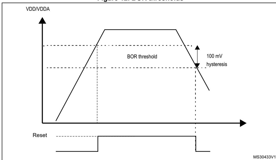
Figure 12 illustrates the BOR (Brownout Reset) thresholds. The top graph shows the VDD/VDDA supply voltage over time. The voltage rises to a plateau and then falls. A horizontal dashed line represents the BOR threshold. A vertical double-headed arrow indicates a 100 mV hysteresis between the rising and falling threshold levels. The bottom graph shows the Reset signal, which is a horizontal line that goes high when VDD/VDDA falls below the BOR threshold and returns low when it rises above it. The identifier MS30433V1 is in the bottom right corner.
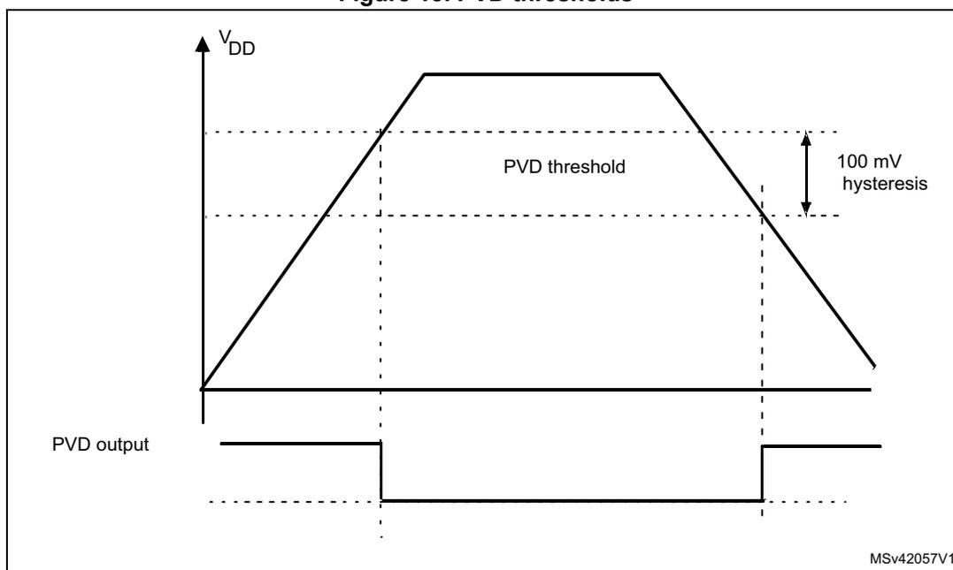
5.2.3 Programmable voltage detector (PVD)
You can use the PVD to monitor the \( V_{DD} \) power supply by comparing it to a threshold selected by the PLS[2:0] bits in the PWR_CR (see Section 5.4.1 ).
The PVD can use an external input analog voltage (PVD_IN) which is compared internally to VREFINT. The PVD_IN (PB7) has to be configured in Analog mode when PLS[2:0] = 111. The PVD is enabled by setting the PVDE bit.
A PVDO flag is available, in the PWR_CSR (see Section 5.4.2 ), to indicate if \( V_{DD} \) is higher or lower than the PVD threshold. This event is internally connected to the EXTI line16 and can generate an interrupt if enabled through the EXTI registers. The PVD output interrupt can be generated when \( V_{DD} \) drops below the PVD threshold and/or when \( V_{DD} \) rises above the PVD threshold depending on EXTI line16 rising/falling edge configuration. As an example the service routine could perform emergency shutdown tasks.
Figure 13. PVD thresholds
5.2.4 Internal voltage reference ( \( V_{REFINT} \) )
The internal reference ( \( V_{REFINT} \) ) provides stable voltage for analog peripherals. The functions managed through the internal voltage reference ( \( V_{REFINT} \) ) are BOR, PVD, ADC, LCD and comparators. Internal voltage reference ( \( V_{REFINT} \) ) is activated if one of the functions: BOR, PVD, ADC, LCD or comparators, is using it.
The internal voltage reference consumption is not negligible, in particular in Stop and Standby mode. To reduce power consumption, the ULP bit (Ultra-low-power) in the PWR_CR register can be set to disable the internal voltage reference. However, in this case, when exiting from the Stop/Standby mode, the functions managed through the internal voltage reference are not reliable during the internal voltage reference startup time (up to 3 ms).
To reduce the wakeup time, the device can exit from Stop/Standby mode without waiting for the internal voltage reference startup time. This is performed by setting the FWU bit (Fast wakeup) in the PWR_CR register before entering Stop/Standby mode.
If the ULP bit is set, the functions that were enabled before entering the Stop/Standby mode are disabled during these modes, and enabled again only after the end of the internal voltage reference startup time whatever FWU value. The VREFINTRDYF flag in the PWR_CSR register indicates that the internal voltage reference is ready.
5.3 Low-power modes
By default, the microcontroller is in Run mode after a system or a power on reset. In Run mode the CPU is clocked by HCLK and the program code is executed. Several low-power modes are available to save power when the CPU does not need to be kept running, for example when waiting for an external event. It is up to the user to select the mode that gives the best compromise between low-power consumption, performance, short startup time and available wakeup sources.
The devices feature five low-power modes:
- • Low-power run mode: regulator in low-power mode, limited clock frequency, limited number of peripherals running
- • Sleep mode: Cortex ® -M3 core stopped, peripherals kept running
- • Low-power sleep mode: Cortex ® -M3 core stopped, limited clock frequency, limited number of peripherals running, regulator in low-power mode, RAM in power down, Flash stopped.
- • Stop mode (all clocks are stopped, regulator running, regulator in low-power mode)
- • Standby mode: V CORE domain powered off
In addition, the power consumption in Run mode can be reduced by one of the following means:
- • Slowing down the system clocks
- • Gating the clocks to the APBx and AHBx peripherals when they are unused.
Table 27. Summary of low-power modes
| Mode name | Entry | Wakeup | Effect on V CORE domain clocks | Effect on V DD domain clocks | Voltage regulator |
|---|---|---|---|---|---|
| Low-power run | LPSDSR and LPRUN bits + Clock setting | The regulator is forced in Main regulator (1.8 V) | None | None | In low-power mode |
| Sleep (Sleep now or Sleep-on-exit) | WFI | Any interrupt | CPU CLK OFF no effect on other clocks or analog clock sources | None | ON |
| WFE | Wakeup event | ||||
| Low-power sleep (Sleep now or Sleep- on-exit) | LPSDSR bits + WFI | Any interrupt | CPU CLK OFF no effect on other clocks or analog clock sources, Flash CLK OFF | None | In low-power mode |
| LPSDSR bits + WFE | Wakeup event | ||||
| Stop | PDDS, LPSDSR bits + SLEEPDEEP bit + WFI or WFE | Any EXTI line (configured in the EXTI registers, internal and external lines) | All V
CORE domain clocks OFF | HSI and HSE and MSI oscillators OFF | In low-power mode |
| Standby | PDDS bit + SLEEPDEEP bit + WFI or WFE | WKUP pin rising edge, RTC alarm (Alarm A or Alarm B), RTC Wakeup event, RTC tamper event, RTC timestamp event, external reset in NRST pin, IWDG reset | OFF |
5.3.1 Behavior of clocks in low-power modes
APB peripheral and DMA clocks can be disabled by software.
Sleep and Low-power sleep modes
The CPU clock is stopped in Sleep and Low-power sleep mode. The memory interface clocks (FLITF and RAM interfaces) and all peripherals clocks can be stopped by software during Sleep. The memory interface (FLITF) clock is stopped and the RAM is in power-down when in Low-power sleep mode. The AHB to APB bridge clocks are disabled by hardware during Sleep/Low-power sleep mode when all the clocks of the peripherals connected to them are disabled.
Stop and Standby modes
The system clock and all high speed clocks are stopped in Stop and Standby modes:
- • PLL is disabled
- • Internal RC 16 MHz (HSI) oscillator is disabled
- • External 1-24 MHz (HSE) oscillator is disabled
- • Internal 65 kHz - 4.2 MHz (MSI) oscillator is disabled
When exiting this mode by interrupt (Stop mode) or by reset (Standby mode), the internal MSI oscillator is selected as system clock. When the device exits Stop mode, the previous MSI configuration (range and trimming value) is kept. When exiting Standby mode, the range and trimming value are reset to the default 2 MHz values.
If a Flash program operation or an access to APB domain is ongoing, the Stop/Standby mode entry is delayed until the Flash memory or the APB access has completed.
The internal regulator can be also kept in the main mode during the Stop mode but the consumption in the Stop mode is much higher and therefore in the Stop mode, it is always implicitly assumed that the regulator is in low-power mode. The only advantage by keeping the regulator in main mode during the Stop mode is a bit shorter wakeup time from the Stop mode.
5.3.2 Slowing down system clocks
In Run mode the speed of the system clocks (SYSCLK, HCLK, PCLK1, PCLK2) can be reduced by programming the prescaler registers. These prescalers can also be used to slow down peripherals before entering Sleep mode.
For more details refer to Section 6.3.3: Clock configuration register (RCC_CFGR) .
5.3.3 Peripheral clock gating
In Run mode, the HCLK and PCLKx for individual peripherals and memories can be stopped at any time to reduce power consumption.
To further reduce power consumption in Sleep mode the peripheral clocks can be disabled prior to executing the WFI or WFE instructions.
Peripheral clock gating is controlled by the AHB peripheral clock enable register (RCC_AHBenR), APB2 peripheral clock enable register (RCC_APB2ENR), APB1 peripheral clock enable register (RCC_APB1ENR) (see Section 6.3.8: AHB peripheral clock enable register (RCC_AHBenR) , Section 6.3.10: APB1 peripheral clock enable register (RCC_APB1ENR) and Section 6.3.9: APB2 peripheral clock enable register (RCC_APB2ENR) ).
Disabling the peripherals clocks in Sleep mode can be performed automatically by resetting the corresponding bit in RCC_AHBLPENR and RCC_APBxLPENR registers (x can 1 or 2).
5.3.4 Low-power run mode (LP run)
To further reduce the consumption when the system is in Run mode, the regulator can be configured in low-power mode. In this mode, the system frequency should not exceed \( f_{MSI} \) range1.
Refer to the product datasheet for more details on voltage regulator and peripherals operating conditions.
Note: To be able to read the RTC calendar register when the APB1 clock frequency is less than seven times the RTC clock frequency ( \( 7 \times RTCLCK \) ), the software must read the calendar time and date registers twice.
If the second read of the RTC_TR gives the same result as the first read, this ensures that the data is correct. Otherwise a third read access must be done.
The Low-power run mode can only be entered when \( V_{CORE} \) is in range 2. In addition, the dynamic voltage scaling must not be used when Low-power run mode is selected. Only Stop and Sleep modes with regulator configured in Low-power mode is allowed when Low-power run mode is selected.
Note: In Low-power run mode, all I/O pins keep the same state as in Run mode.
Entering Low-power run mode
To enter Low-power run mode proceed as follows:
- • Each digital IP clock must be enabled or disabled by using the RCC_APBxENR and RCC_AHBENR registers.
- • The frequency of the system clock must be decreased to not exceed the frequency of \( f_{MSI} \) range1.
- • The regulator is forced in low-power mode by software (LPRUN and LPSDSR bits set)
Exiting Low-power run mode
To exit Low-power run mode proceed as follows:
- • The regulator is forced in Main regulator mode by software.
- • The Flash memory is switched on, if needed.
- • The frequency of the clock system can be increased.
5.3.5 Sleep mode
Entering Sleep mode
The Sleep mode is entered by executing the WFI (Wait For Interrupt) or WFE (Wait for Event) instructions. Two options are available to select the Sleep mode entry mechanism, depending on the SLEEPONEXIT bit in the Cortex ® -M3 System Control register:
- • Sleep-now: if the SLEEPONEXIT bit is cleared, the MCU enters Sleep mode as soon as WFI or WFE instruction is executed.
- • Sleep-on-exit: if the SLEEPONEXIT bit is set, the MCU enters Sleep mode as soon as it exits the lowest priority ISR.
Note: In Sleep mode, all I/O pins keep the same state as in Run mode.
Refer to Table 28: Sleep-now and Table 29: Sleep-on-exit for details on how to enter Sleep mode.
Exiting Sleep mode
If the WFI instruction is used to enter Sleep mode, any peripheral interrupt acknowledged by the nested vectored interrupt controller (NVIC) can wake up the device from Sleep mode.
If the WFE instruction is used to enter Sleep mode, the MCU exits Sleep mode as soon as an event occurs. The wakeup event can be generated either by:
- • Enabling an interrupt in the peripheral control register but not in the NVIC, and enabling the SEVONPEND bit in the Cortex®-M3 System Control register. When the MCU resumes from WFE, the peripheral interrupt pending bit and the peripheral NVIC IRQ channel pending bit (in the NVIC interrupt clear pending register) have to be cleared.
- • Or configuring an external or internal EXTI line in event mode. When the CPU resumes from WFE, it is not necessary to clear the peripheral interrupt pending bit or the NVIC IRQ channel pending bit as the pending bit corresponding to the event line is not set.
This mode offers the lowest wakeup time as no time is wasted in interrupt entry/exit.
Refer to Table 28: Sleep-now and Table 29: Sleep-on-exit for more details on how to exit Sleep mode.
Table 28. Sleep-now
| Sleep-now mode | Description |
|---|---|
| Mode entry | – Clear all interrupt pending bits WFI (Wait for Interrupt) or WFE (Wait for Event) while: – SLEEPDEEP = 0 and – SLEEPONEXIT = 0 Refer to the Cortex®-M3 System Control register. |
| Mode exit | If WFI was used for entry: Interrupt: Refer to Table 49: Vector table (Cat.1 and Cat.2 devices) If WFE was used for entry Wakeup event: Refer to Section 10.2.3: Wakeup event management |
| Wakeup latency | None |
Table 29. Sleep-on-exit
| Sleep-on-exit | Description |
|---|---|
| Mode entry | – Clear all interrupt pending bits WFI (wait for interrupt) while: – SLEEPDEEP = 0 and – SLEEPONEXIT = 1 Refer to the Cortex®-M3 System Control register. |
| Mode exit | Interrupt: refer to
Table 49: Vector table (Cat.1 and Cat.2 devices)
, Table 50: Vector table (Cat.3 devices) and Table 51: Vector table (Cat.4, Cat.5 and Cat.6 devices) . |
| Wakeup latency | None |
5.3.6 Low-power sleep mode (LP sleep)
Entering Low-power sleep mode
The Low-power sleep mode is entered by configuring the voltage regulator in low-power mode, and by executing the WFI (wait for interrupt) or WFE (wait for event) instructions. In this mode, the Flash memory is not available but the RAM memory remains available.
In this mode, the system frequency should not exceed f_MSI range1.
Refer to product datasheet for more details on voltage regulator and peripherals operating conditions.
Low-power sleep mode can only be entered when V CORE is in range 2.
Note: To be able to read the RTC calendar register when the APB1 clock frequency is less than seven times the RTC clock frequency (7*RTCCLK), the software must read the calendar time and date registers twice.
If the second read of the RTC_TR gives the same result as the first read, this ensures that the data is correct. Otherwise a third read access must be done.
Two options are available to select the Sleep low-power mode entry mechanism, depending on the SLEEPONEXIT bit in the Cortex ® -M3 System Control register:
- • Sleep-now: if the SLEEPONEXIT bit is cleared, the MCU enters Sleep mode as soon as WFI or WFE instruction is executed.
- • Sleep-on-exit: if the SLEEPONEXIT bit is set, the MCU enters Sleep mode as soon as it exits the lowest priority ISR.
To enter Low-power sleep mode, proceed as follows:
- • The Flash memory can be switched off by using the control bits (SLEEP_PD in the FLASH_ACR register. For more details refer to Section 3: Flash program memory and data EEPROM (FLASH) ). This reduces power consumption but increases the wake-up time.
- • Each digital IP clock must be enabled or disabled by using the RCC_APBxENR and RCC_AHBENR registers. To keep it running in the Low-power sleep mode the digital IP clock have to be enabled in RCC_APBxLPENR and RCC_AHBLPENR.
- • The frequency of the system clock must be decreased.
- • The regulator is forced in low-power mode by software (LPSDSR bits set).
- • A WFI/WFE instruction must be executed to enter in Sleep mode.
Note: In Low-power sleep mode, all I/O pins keep the same state as in Run mode.
Refer to Table 30: Sleep-now and Table 31: Sleep-on-exit for details on how to enter Low-power sleep mode.
Exiting Low-power sleep mode
If the WFI instruction was used to enter Low-power sleep mode, any peripheral interrupt acknowledged by the nested vectored interrupt controller (NVIC) can wake up the device from Low-power sleep mode.
If the WFE instruction was used to enter Low-power sleep mode, the MCU exits Sleep mode as soon as an event occurs. The wakeup event can be generated:
- • By enabling an interrupt in the peripheral control register but not in the NVIC, and by enabling the SEVONPEND bit in the Cortex ® -M3 System Control register. When the
MCU resumes from WFE, the peripheral interrupt pending bit and the peripheral NVIC IRQ channel pending bit in the NVIC interrupt clear pending register must be cleared.
- Or by configuring an external or internal EXTI line in event mode. When the CPU resumes from WFE, it is not necessary to clear the peripheral interrupt pending bit or the NVIC IRQ channel pending bit as the pending bit corresponding to the event line is not set.
When exiting Low-power sleep mode by issuing an interrupt or a wakeup event, the regulator is configured in Main regulator mode, the Flash memory is switched on (if necessary), and the system clock can be increased.
When the voltage regulator operates in low-power mode, an additional startup delay is incurred when waking up from Low-power sleep mode.
Refer to Table 30: Sleep-now and Table 31: Sleep-on-exit for more details on how to exit Sleep low-power mode.
Table 30. Sleep-now
| Sleep-now mode | Description |
|---|---|
| Mode entry | Voltage regulator in low-power mode and the Flash memory switched off WFI (Wait for Interrupt) or WFE (wait for event) while: – SLEEPDEEP = 0 and – SLEEPONEXIT = 0 Refer to the Cortex®-M3 System Control register. |
| Mode exit | Voltage regulator in Main regulator mode and the Flash memory switched on If WFI was used for entry: Interrupt: Refer to Table 49: Vector table (Cat.1 and Cat.2 devices) If WFE was used for entry Wakeup event: Refer to Section 10.2.3: Wakeup event management |
| Wakeup latency | Regulator wakeup time from low-power mode |
Table 31. Sleep-on-exit
| Sleep-on-exit | Description |
|---|---|
| Mode entry | Voltage regulator in low-power mode and the Flash memory switched off WFI (wait for interrupt) while: – SLEEPDEEP = 0 and – SLEEPONEXIT = 1 Refer to the Cortex®-M3 System Control register. |
| Mode exit | Interrupt: refer to
Table 49: Vector table (Cat.1 and Cat.2 devices)
, Table 50: Vector table (Cat.3 devices) and Table 51: Vector table (Cat.4, Cat.5 and Cat.6 devices) . |
| Wakeup latency | regulator wakeup time from low-power mode |
5.3.7 Stop mode
The Stop mode is based on the Cortex®-M3 deepsleep mode combined with peripheral clock gating. The voltage regulator can be configured either in normal or low-power mode.
In Stop mode, all clocks in the V CORE domain are stopped, the PLL, the MSI, the HSI and the HSE RC oscillators are disabled. Internal SRAM and register contents are preserved.
To get the lowest consumption in Stop mode, the internal Flash memory also enters low-power mode. When the Flash memory is in power down mode, an additional startup delay is incurred when waking up from Stop mode.
To minimize the consumption In Stop mode, V REFINT , the BOR, PVD, and temperature sensor can be switched off before entering the Stop mode. They can be switched on again by software after exiting the Stop mode using the ULP bit in the PWR_CR register.
Note: In Stop mode, all I/O pins keep the same state as in Run mode.
Entering the Stop mode
Refer to Table 32 for details on how to enter the Stop mode.
Note: If the application needs to disable the external clock before entering the stop mode, the HSEON bit must be first disabled and the system clock switched to HSI.
Otherwise, if the HSEON bit is kept enabled while external clock (external oscillator) can be removed before entering stop mode, the clock security system (CSS) feature must be enabled to detect any external oscillator failure and avoid a malfunction behavior when entering stop mode.
To further reduce power consumption in Stop mode, the internal voltage regulator can be put in low-power mode. This is configured by the LPSDSR bit in the PWR_CR register (see Section 5.4.1 ).
If Flash memory programming or an access to the APB domain is ongoing, the Stop mode entry is delayed until the memory or APB access has completed.
In Stop mode, the following features can be selected by programming individual control bits:
- • Independent watchdog (IWDG): the IWDG is started by writing to its Key register or by hardware option. Once started it cannot be stopped except by a Reset. Refer to Section 21.3 in Section 21: Independent watchdog (IWDG) .
- • Real-time clock (RTC): this is configured by the RTCEN bit in the RCC_CSR register (see Section 6.3.14 ).
- • Internal RC oscillator (LSI RC): this is configured by the LSION bit in the RCC_CSR register.
- • External 32.768 kHz oscillator (LSE OSC): this is configured by the LSEON bit in the RCC_CSR register.
The ADC, DAC or LCD can also consume power in Stop mode, unless they are disabled before entering it. To disable them, the ADON bit in the ADC_CR2 register and the ENx bit in the DAC_CR register must both be written to 0.
Exiting the Stop mode
Refer to Table 32 for more details on how to exit Stop mode.
When exiting Stop mode by issuing an interrupt or a wakeup event, the MSI RC oscillator is selected as system clock.
When the voltage regulator operates in low-power mode, an additional startup delay is incurred when waking up from Stop mode. By keeping the internal regulator ON during Stop mode, the consumption is higher although the startup time is reduced.
Table 32. Stop mode
| Stop mode | Description |
|---|---|
| Mode entry | WFI (Wait for Interrupt) or WFE (Wait for Event) while:
Note: To enter the Stop mode, all EXTI Line pending bits (in EXTI pending register (EXTI_PR) ), all peripherals interrupt pending bits, the RTC Alarm (Alarm A and Alarm B), RTC wakeup, RTC tamper, and RTC time-stamp flags, must be reset. Otherwise, the Stop mode entry procedure is ignored and program execution continues. |
| Mode exit | If WFI was used for entry: Any EXTI Line configured in Interrupt mode (the corresponding EXTI Interrupt vector must be enabled in the NVIC). Refer to Table 49: Vector table (Cat.1 and Cat.2 devices) , Table 50: Vector table (Cat.3 devices) and Table 51: Vector table (Cat.4, Cat.5 and Cat.6 devices) . If WFE was used for entry: Any EXTI Line configured in event mode. Refer to Section 10.2.3: Wakeup event management on page 238 |
| Wakeup latency | MSI RC wakeup time + regulator wakeup time from Low-power mode + FLASH wakeup time |
5.3.8 Standby mode
The Standby mode allows the application to achieve the lowest power consumption. It is based on the Cortex®-M3 deepsleep mode, with the voltage regulator disabled. The V CORE domain is consequently powered off. The PLL, the MSI, the HSI oscillator and the HSE oscillator are also switched off. SRAM and register contents are lost except for the RTC registers, RTC backup registers and Standby circuitry (see Figure 8 ).
Entering the Standby mode
Refer to Table 33 for more details on how to enter Standby mode.
In Standby mode, the following features can be selected by programming individual control bits:
- • Independent watchdog (IWDG): the IWDG is started by writing to its Key register or by hardware option. Once started it cannot be stopped except by a reset. Refer to Section 21.3: IWDG functional description on page 549 .
- • Real-time clock (RTC): this is configured by the RTCEN bit in the RCC_CSR register (see Section 6.3.14 ).
- • Internal RC oscillator (LSI RC): this is configured by the LSION bit in the RCC_CSR register.
- • External 32.768 kHz oscillator (LSE OSC): this is configured by the LSEON bit in the RCC_CSR register.
Exiting the Standby mode
The microcontroller exits Standby mode when an external Reset (NRST pin), an IWDG Reset, a rising edge on WKUP pins (WKUP1, WKUP2 or WKUP3), an RTC alarm, a tamper event, or a time-stamp event is detected. All registers are reset after wakeup from Standby except for PWR power control/status register (PWR_CSR) .
After waking up from Standby mode, program execution restarts in the same way as after a Reset (boot pins sampling, vector reset is fetched, etc.). The SBF status flag in the PWR_CSR register (see Section 5.4.2 ) indicates that the MCU was in Standby mode.
Refer to Table 33 for more details on how to exit Standby mode.
Table 33. Standby mode
| Standby mode | Description |
|---|---|
| Mode entry | WFI (Wait for Interrupt) or WFE (Wait for Event) while:
|
| Mode exit | WKUP pin rising edge, RTC alarm (Alarm A and Alarm B), RTC wakeup, tamper event, time-stamp event, external reset in NRST pin, IWDG reset. |
| Wakeup latency | Reset phase |
I/O states in Standby mode
In Standby mode, all I/O pins are high impedance except for:
- • Reset pad (still available)
- • RTC_AF1 pin (PC13) if configured for Wakeup pin 2 (WKUP2), tamper, time-stamp, RTC Alarm out, or RTC clock calibration out.
- • WKUP pin 1 (PA0) and WKUP pin 3 (PE6), if enabled.
Debug mode
By default, the debug connection is lost if the application puts the MCU in Stop or Standby mode while the debug features are used. This is due to the fact that the Cortex®-M3 core is no longer clocked.
However, by setting some configuration bits in the DBGMCU_CR register, the software can be debugged even when using the low-power modes extensively. For more details, refer to Section 30.16.1: Debug support for low-power modes .
5.3.9 Waking up the device from Stop and Standby modes using the RTC and comparators
The MCU can be woken up from low-power mode by an RTC Alarm event, an RTC Wakeup event, a tamper event, a time-stamp event, or a comparator event, without depending on an external interrupt (Auto-wakeup mode).
These RTC alternate functions can wake up the system from Stop and Standby low-power modes while the comparator events can only wake up the system from Stop mode.
The system can also wake up from low-power modes without depending on an external interrupt (Auto-wakeup mode) by using the RTC alarm or the RTC wakeup events.
The RTC provides a programmable time base for waking up from Stop or Standby mode at regular intervals. For this purpose, two of the three alternative RTC clock sources can be selected by programming the RTCSEL[1:0] bits in the RCC_CSR register (see Section 6.3.14 ):
- • Low-power 32.768 kHz external crystal oscillator (LSE OSC).
This clock source provides a precise time base with very low-power consumption (less than 1 µA added consumption in typical conditions) - • Low-power internal RC oscillator (LSI RC)
This clock source has the advantage of saving the cost of the 32.768 kHz crystal. This internal RC Oscillator is designed to use minimum power consumption.
RTC auto-wakeup (AWU) from the Stop mode
- • To wake up from the Stop mode with an RTC alarm event, it is necessary to:
- a) Configure the EXTI Line 17 to be sensitive to rising edges (Interrupt or Event modes)
- b) Enable the RTC Alarm interrupt in the RTC_CR register
- c) Configure the RTC to generate the RTC alarm
- • To wake up from the Stop mode with an RTC Tamper or time stamp event, it is necessary to:
- a) Configure the EXTI Line 19 to be sensitive to rising edges (Interrupt or Event modes)
- b) Enable the RTC TimeStamp Interrupt in the RTC_CR register or the RTC Tamper Interrupt in the RTC_TCR register
- c) Configure the RTC to detect the tamper or time stamp event
- • To wake up from the Stop mode with an RTC Wakeup event, it is necessary to:
- a) Configure the EXTI Line 20 to be sensitive to rising edges (Interrupt or Event modes)
- b) Enable the RTC Wakeup Interrupt in the RTC_CR register
- c) Configure the RTC to generate the RTC Wakeup event
RTC auto-wakeup (AWU) from the Standby mode
- • To wake up from the Standby mode with an RTC alarm event, it is necessary to:
- a) Enable the RTC Alarm interrupt in the RTC_CR register
- b) Configure the RTC to generate the RTC alarm
- • To wake up from the Standby mode with an RTC Tamper or time stamp event, it is necessary to:
- a) Enable the RTC TimeStamp Interrupt in the RTC_CR register or the RTC Tamper Interrupt in the RTC_TCR register
- b) Configure the RTC to detect the tamper or time stamp event
- • To wake up from the Standby mode with an RTC Wakeup event, it is necessary to:
- a) Enable the RTC Wakeup Interrupt in the RTC_CR register
- b) Configure the RTC to generate the RTC Wakeup event
Comparator auto-wakeup (AWU) from the Stop mode
- • To wake up from the Stop mode with a comparator 1 or comparator 2 wakeup event, it is necessary to:
- a) Configure the EXTI Line 21 for comparator 1 or EXTI Line 22 for comparator 2 (Interrupt or Event mode) to be sensitive to the selected edges (falling, rising or falling and rising)
- b) Configure the comparator to generate the event
5.4 Power control registers
The peripheral registers have to be accessed by half-words (16-bit) or words (32-bit).
5.4.1 PWR power control register (PWR_CR)
Address offset: 0x00
Reset value: 0x0000 1000 (reset by wakeup from Standby mode)
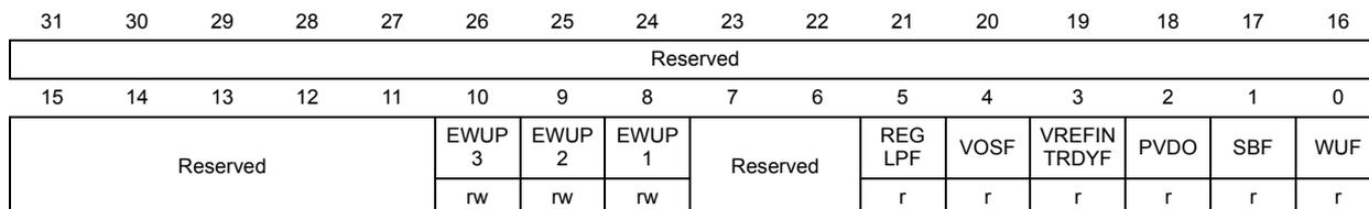
| 31 | 30 | 29 | 28 | 27 | 26 | 25 | 24 | 23 | 22 | 21 | 20 | 19 | 18 | 17 | 16 |
|---|---|---|---|---|---|---|---|---|---|---|---|---|---|---|---|
| Reserved | |||||||||||||||
| 15 | 14 | 13 | 12 | 11 | 10 | 9 | 8 | 7 | 6 | 5 | 4 | 3 | 2 | 1 | 0 |
| Res. | LPRUN | Res. | VOS[1:0] | FWU | ULP | DBP | PLS[2:0] | PVDE | CSBF | CWUF | PDDS | LPSDSR | |||
| rw | rw | rw | rw | rw | rw | rw | rw | rw | rw | rc_w1 | rc_w1 | rw | rw | ||
Bits 31:15 Reserved, always read as 0.
Bit 14 LPRUN : Low-power run mode
When LPRUN bit is set together with the LPSDSR bit, the regulator is switched from main mode to low-power mode. Otherwise, it remains in main mode. The regulator goes back to operate in main mode when LPRUN is reset.
It is forbidden to reset LPSDSR when the MCU is in Low-power run mode. LPSDSR is used as a prepositioning for the entry into low-power mode, indicating to the system which configuration of the regulator is selected when entering Low-power mode. The LPSDSR bit must be set before the LPRUN bit is set. LPSDSR can be reset only when LPRUN bit=0.
0: Voltage regulator in main mode in Low-power run mode
1: Voltage regulator in low-power mode in Low-power run mode
Bits 13 Reserved, must be kept at reset value.
Bits 12:11 VOS[1:0] : Voltage scaling range selection
These bits are used to select the internal regulator voltage range.
Before resetting the power interface by resetting the PWRRST bit in the RCC_APB1RSTR register, these bits have to be set to "10" and the frequency of the system has to be configured accordingly.
00: forbidden (bits are unchanged and keep the previous value, no voltage scaling range changed)
01: 1.8 V (range 1)
10: 1.5 V (range 2)
11: 1.2 V (range 3)
Bit 10 FWU : Fast wakeup
This bit works in conjunction with ULP bit.
If ULP = 0, FWU is ignored
If ULP = 1 and FWU = 1: V REFINT startup time is ignored when exiting from low-power mode.
The VREFINTRDYF flag in the PWR_CSR register indicates when the V REFINT is ready again.
If ULP=1 and FWU = 0: Exiting from low-power mode occurs only when the V REFINT is ready (after its startup time). This bit is not reset by resetting the PWRRST bit in the RCC_APB1RSTR register.
0: Low-power modes exit occurs only when V REFINT is ready
1: V REFINT start up time is ignored when exiting low-power modes
Bit 9 ULP: Ultra-low-power modeWhen set, the \( V_{REFINT} \) is switched off in low-power mode. This bit is not reset by resetting the PWRRST bit in the RCC_APB1RSTR register.
0: \( V_{REFINT} \) is on in low-power mode
1: \( V_{REFINT} \) is off in low-power mode
Bit 8 DBP: Disable backup write protectionIn reset state, the RTC, RTC backup registers and RCC CSR register are protected against parasitic write access. This bit must be set to enable write access to these registers.
0: Access to RTC, RTC Backup and RCC CSR registers disabled
1: Access to RTC, RTC Backup and RCC CSR registers enabled
Note: If the HSE divided by 2, 4, 8 or 16 is used as the RTC clock, this bit must remain set to 1.
Bits 7:5 PLS[2:0]: PVD level selectionThese bits are written by software to select the voltage threshold detected by the power voltage detector:
000: 1.9 V
001: 2.1 V
010: 2.3 V
011: 2.5 V
100: 2.7 V
101: 2.9 V
110: 3.1 V
111: External input analog voltage (Compare internally to \( V_{REFINT} \) )
PVD_IN input (PB7) has to be configured as analog input when PLS[2:0] = 111.
Note: Refer to the electrical characteristics of the datasheet for more details.
Bit 4 PVDE: Power voltage detector enableThis bit is set and cleared by software.
0: PVD disabled
1: PVD enabled
Bit 3 CSBF: Clear standby flagThis bit is always read as 0.
0: No effect
1: Clear the SBF Standby flag (write).
Bit 2 CWUF : Clear wakeup flagThis bit is always read as 0.
0: No effect
1: Clear the WUF Wakeup flag after 2 system clock cycles
Bit 1 PDDS : Power down deepsleepThis bit is set and cleared by software.
0: Enter Stop mode when the CPU enters deepsleep.
1: Enter Standby mode when the CPU enters deepsleep.
Bit 0 LPDSR : Low-power deepsleep/sleep/low-power run– DeepSleep/Sleep modes
When this bit is set, the regulator switches in low-power mode when the CPU enters sleep or deepsleep mode. The regulator goes back to main mode when the CPU exits from these modes.
– Low-power run mode
When this bit is set, the regulator switches in low-power mode when the bit LPRUN is set. The regulator goes back to main mode when the bit LPRUN is reset.
This bit is set and cleared by software.
0: Voltage regulator on during deepsleep/Sleep/Low-power run mode
1: Voltage regulator in low-power mode during deepsleep/Sleep/Low-power run mode
5.4.2 PWR power control/status register (PWR_CSR)
Address offset: 0x04
Reset value: 0x0000 0008 (not reset by wakeup from Standby mode)
Additional APB cycles are needed to read this register versus a standard APB read.
| 31 | 30 | 29 | 28 | 27 | 26 | 25 | 24 | 23 | 22 | 21 | 20 | 19 | 18 | 17 | 16 |
| Reserved | |||||||||||||||
| 15 | 14 | 13 | 12 | 11 | 10 | 9 | 8 | 7 | 6 | 5 | 4 | 3 | 2 | 1 | 0 |
| Reserved | EWUP 3 | EWUP 2 | EWUP 1 | Reserved | REG LPF | VOSF | VREFIN TRDYF | PVDO | SBF | WUF | |||||
| rw | rw | rw | r | r | r | r | r | r | |||||||
Bits 31:11 Reserved, must be kept at reset value.
Bit 10 EWUP3 : Enable WKUP pin 3
This bit is set and cleared by software.
0: WKUP pin 3 is used for general purpose I/Os. An event on the WKUP pin 3 does not wakeup the device from Standby mode.
1: WKUP pin 3 is used for wakeup from Standby mode and forced in input pull down configuration (rising edge on WKUP pin 3 wakes-up the system from Standby mode).
Note: This bit is reset by a system reset.
Bit 9 EWUP2 : Enable WKUP pin 2
This bit is set and cleared by software.
0: WKUP pin 2 is used for general purpose I/Os. An event on the WKUP pin 2 does not wakeup the device from Standby mode.
1: WKUP pin 2 is used for wakeup from Standby mode and forced in input pull down configuration (rising edge on WKUP pin 2 wakes-up the system from Standby mode).
Note: This bit is reset by a system reset.
Bit 8 EWUP1 : Enable WKUP pin 1
This bit is set and cleared by software.
0: WKUP pin 1 is used for general purpose I/Os. An event on the WKUP pin 1 does not wakeup the device from Standby mode.
1: WKUP pin 1 is used for wakeup from Standby mode and forced in input pull down configuration (rising edge on WKUP pin 1 wakes-up the system from Standby mode).
Note: This bit is reset by a system reset.
Bits 7:6 Reserved, must be kept at reset value.
Bit 5 REGLPF : Regulator LP flag
This bit is set by hardware when the MCU is in Low-power run mode.
When the MCU exits from Low-power run mode, this bit stays at 1 until the regulator is ready in main mode. A polling on this bit is recommended to wait for the regulator main mode. This bit is reset by hardware when the regulator is ready.
0: Regulator is ready in main mode
1: Regulator voltage is in low-power mode
Bit 4 VOSF : Voltage Scaling select flagA delay is required for the internal regulator to be ready after the voltage range is changed. The VOSF bit indicates that the regulator has reached the voltage level defined with bits VOS of PWR_CR register.
This bit is set when VOS[1:0] in PWR_CR register change.
It is reset once the regulator is ready.
0: Regulator is ready in the selected voltage range
1: Regulator voltage output is changing to the required VOS level.
Bit 3 VREFINTRDYF : Internal voltage reference (V REFINT ) ready flagThis bit indicates the state of the internal voltage reference, V REFINT .
0: V REFINT is OFF
1: V REFINT is ready
Bit 2 PVDO : PVD outputThis bit is set and cleared by hardware. It is valid only if PVD is enabled by the PVDE bit.
0: V DD is higher than the PVD threshold selected with the PLS[2:0] bits.
1: V DD is lower than the PVD threshold selected with the PLS[2:0] bits.
Note: The PVD is stopped by Standby mode. For this reason, this bit is equal to 0 after Standby or reset until the PVDE bit is set.
Bit 1 SBF : Standby flagThis bit is set by hardware and cleared only by a POR/PDR (power on reset/power down reset) or by setting the CSBF bit in the PWR power control register (PWR_CR)
0: Device has not been in Standby mode
1: Device has been in Standby mode
Bit 0 WUF : Wakeup flagThis bit is set by hardware and cleared by a system reset or by setting the CWUF bit in the PWR power control register (PWR_CR)
0: No wakeup event occurred
1: A wakeup event was received from the WKUP pin or from the RTC alarm (Alarm A or Alarm B), RTC Tamper event, RTC TimeStamp event or RTC Wakeup).
Note: An additional wakeup event is detected if the WKUP pins are enabled (by setting the EWUPx (x=1, 2, 3) bits) when the WKUP pin levels are already high.
5.4.3 PWR register map
The following table summarizes the PWR registers. The reserved memory areas are highlighted in gray in the table.
Table 34. PWR - register map and reset values
| Offset | Register | 31 | 30 | 29 | 28 | 27 | 26 | 25 | 24 | 23 | 22 | 21 | 20 | 19 | 18 | 17 | 16 | 15 | 14 | 13 | 12 | 11 | 10 | 9 | 8 | 7 | 6 | 5 | 4 | 3 | 2 | 1 | 0 |
|---|---|---|---|---|---|---|---|---|---|---|---|---|---|---|---|---|---|---|---|---|---|---|---|---|---|---|---|---|---|---|---|---|---|
| 0x000 | PWR_CR | Reserved | LPRUN | Reserved | VOS [1:0] | FWU | ULP | DBP | PLS[2:0] | PVDE | CSBF | CWUF | PDDS | LPSDSR | |||||||||||||||||||
| Reset value | 0 | 1 | 0 | 0 | 0 | 0 | 0 | 0 | 0 | 0 | 0 | 0 | 0 | 0 | |||||||||||||||||||
Table 34. PWR - register map and reset values (continued)
| Offset | Register | 31 | 30 | 29 | 28 | 27 | 26 | 25 | 24 | 23 | 22 | 21 | 20 | 19 | 18 | 17 | 16 | 15 | 14 | 13 | 12 | 11 | 10 | 9 | 8 | 7 | 6 | 5 | 4 | 3 | 2 | 1 | 0 |
|---|---|---|---|---|---|---|---|---|---|---|---|---|---|---|---|---|---|---|---|---|---|---|---|---|---|---|---|---|---|---|---|---|---|
| 0x004 | PWR_CSR | Reserved | EWUP3 | EWUP2 | EWUP1 | Reserved | REGLPF | VOSF | VREFINTRDYF | PVDO | SBF | WUF | |||||||||||||||||||||
| Reset value | 0 | 0 | 0 | 0 | 0 | 1 | 0 | 0 | 0 | ||||||||||||||||||||||||
Refer to Table 5 on page 47 for the register boundary addresses.