3. Flash program memory and data EEPROM (FLASH)
3.1 NVM introduction
- • Up to 512 Kbytes of Flash program memory
- • Memory organization (dual bank; for Cat.4, Cat.5 and Cat.6 devices only):
- – Up to 512 Kbytes of Flash program memory and up to 16 Kbytes of data EEPROM
- – Up to 8 Kbytes of system memory and up to 64 bytes of option bytes
Each bank in dual bank devices is organized as follows:
- – 192/256 Kbytes of program memory and 6/8 Kbytes of data (for Cat.4, Cat.5 and Cat.6 devices only)
- – 4 Kbytes of system memory, 32 bytes of option bytes
Flash memory interface (FLITF) features:
- • Flash memory read operations: read access is performed by 64 or 32 bits
- • Flash memory program/erase operations
- • Read while write (RWW) from one bank to the other
- • Read/write protection
- • Write access is performed by 32 bits
- • Option byte loader reset
- • Low power mode:
- – Flash memory in Power down mode when the STM32L1xxxx is in the Standby mode or the Stop mode
- – Flash memory can be placed in Power down or Idle mode when the STM32L1xxxx is in the Sleep mode
- – Flash memory can be placed in Power down or Idle mode when the STM32L1xxxx is in the Run mode
Note: The DMA can only access Flash memory module with read operations.
Note: Code execution is not possible from Data EEPROM.
3.2 NVM organization
The memory is organized as Program memory blocks, data EEPROM blocks and information blocks. Table 8 , Table 9 , Table 10 and Table 11 show the memory organization (the maximum configuration for given product category). See device datasheet for Flash program memory size and data EEPROM memory size availability.
The Flash program memory block is divided into sectors of 4 Kbytes each, and each sector is further split up into 16 pages of 256 bytes each. The sector is the write protection granularity. The pages are the erase granularity for the program memory block.
The Flash program memory pages can be written using a half page programming or a fast word programming operation.
Data EEPROM can be erased and written by:
- • Double word
- • Word/ Fast word
- • Half word / Fast half word
- • Byte / Fast byte
During a write/erase operation to the NVM (except Half Page programming or Double-word erase/write), any attempt to read the same bank of NVM stalls the bus. The read operation is executed correctly once the programming operation is completed. This means that code or data fetches cannot be performed while a write/erase operation is ongoing in the same bank.
For more details, refer to Section 3.4.2: Erasing memory on page 64 and Section 3.4.3: Programming memory on page 65 .
Table 8. NVM module organization (Cat.1 and Cat.2 devices)
| Block | Name | Memory addresses | Size | |
|---|---|---|---|---|
| Program memory | Sector 0 | Page 0 | 0x0800 0000 - 0x0800 00FF | 256 bytes |
| Page 1 | 0x0800 0100 - 0x0800 01FF | 256 bytes | ||
| Page 2 | 0x0800 0200 - 0x0800 02FF | 256 bytes | ||
| Page 3 | 0x0800 0300 - 0x0800 03FF | 256 bytes | ||
| Page 4 to 7 | 0x0800 0400 - 0x0800 07FF | 1 Kbyte | ||
| Page 8 to 11 | 0x0800 0800 - 0x0800 0BFF | 1 Kbyte | ||
| Page 12 to 15 | 0x0800 0C00 - 0x0800 0FFF | 1 Kbyte | ||
| Sector 1 | 0x0800 1000 - 0x0800 1FFF | 4 Kbytes | ||
| Sector 2 | 0x0800 2000 - 0x0800 2FFF | 4 Kbytes | ||
| Sector 3 | 0x0800 3000 - 0x0800 3FFF | 4 Kbytes | ||
| . | . | . | ||
| . | . | . | ||
| . | . | . | ||
| Sector 30 | 0x0801 E000 - 0x0801 EFFF | 4 Kbytes | ||
| Sector 31 | 0x0801 F000 - 0x0801 FFFF | 4 Kbytes | ||
| Data EEPROM | 0x0808 0000 - 0x0808 0FFF | 4096 bytes | ||
Table 8. NVM module organization (Cat.1 and Cat.2 devices) (continued)
| Block | Name | Memory addresses | Size | |
|---|---|---|---|---|
| Information block | System memory | Page 0 | 0x1FF0 0000 - 0x1FF0 00FF | 256 bytes |
| Page 1 | 0x1FF0 0100 - 0x1FF0 01FF | 256 bytes | ||
| Page 2 | 0x1FF0 0200 - 0x1FF0 02FF | 256 bytes | ||
| Page 3 | 0x1FF0 0300 - 0x1FF0 03FF | 256 bytes | ||
| . | . | . | ||
| . | . | . | ||
| Page 15 | 0x1FF0 0F00 - 0x1FF0 0FFF | 256 bytes | ||
| Option bytes | 0x1FF8 0000 - 0x1FF8 001F | 32 bytes | ||
| Factory information | 0x1FF8 0020 - 0x1FF8 00FF | 224 bytes | ||
Table 9. NVM module organization (Cat.3 devices)
| Block | Name | Memory addresses | Size | |
|---|---|---|---|---|
| Program memory | Sector 0 | Page 0 | 0x0800 0000 - 0x0800 00FF | 256 bytes |
| Page 1 | 0x0800 0100 - 0x0800 01FF | 256 bytes | ||
| Page 2 | 0x0800 0200 - 0x0800 02FF | 256 bytes | ||
| Page 3 | 0x0800 0300 - 0x0800 03FF | 256 bytes | ||
| Page 4 to 7 | 0x0800 0400 - 0x0800 07FF | 1 Kbyte | ||
| Page 8 to 11 | 0x0800 0800 - 0x0800 0BFF | 1 Kbyte | ||
| Page 12 to 15 | 0x0800 0C00 - 0x0800 0FFF | 1 Kbyte | ||
| Sector 1 | Page 16 to 31 | 0x0800 1000 - 0x0800 1FFF | 4 Kbytes | |
| Sector 2 | Page 32 to 47 | 0x0800 2000 - 0x0800 2FFF | 4 Kbytes | |
| Sector 3 | Page 48 to 63 | 0x0800 3000 - 0x0800 3FFF | 4 Kbytes | |
| . | . | . | . | |
| . | . | . | . | |
| . | . | . | . | |
| Sector 30 | Page 478 to 495 | 0x0801 E000 - 0x0801 EFFF | 4 Kbytes | |
| Sector 31 | Page 496 to 511 | 0x0801 F000 - 0x0801 FFFF | 4 Kbytes | |
| Sector 32 to Sector 47 | Page 512 to 767 | 0x0802 0000 - 0x0802 FFFF | 64 Kbytes | |
| Sector 48 to Sector 63 | Page 768 to 1023 | 0x0803 0000 - 0x0803 FFFF | 64 Kbytes | |
| Data EEPROM | 0x0808 0000 - 0x0808 1FFF | 8 Kbytes | ||
Table 9. NVM module organization (Cat.3 devices) (continued)
| Block | Name | Memory addresses | Size | |
|---|---|---|---|---|
| Information Block | System memory | Page 0 | 0x1FF0 0000 - 0x1FF0 00FF | 256 bytes |
| Page 1 | 0x1FF0 0100 - 0x1FF0 01FF | 256 bytes | ||
| Page 2 | 0x1FF0 0200 - 0x1FF0 02FF | 256 bytes | ||
| Page 3 | 0x1FF0 0300 - 0x1FF0 03FF | 256 bytes | ||
| . | . | . | ||
| . | . | . | ||
| . | . | . | ||
| Page 15 | 0x1FF0 0F00 - 0x1FF0 0FFF | 256 bytes | ||
| Page 16 to 31 | 0x1FF0 1000 - 0x1FF0 1FFF | 4 Kbytes | ||
| Option bytes | 0x1FF8 0000 - 0x1FF8 001F | 32 bytes | ||
| Factory information | 0x1FF8 0020 - 0x1FF8 00FF | 224 bytes | ||
Table 10. NVM module organization (Cat.4 devices)
| Block | Name | Memory addresses | Size | |
|---|---|---|---|---|
| Program memory bank 1 | Sector 0 | Page 0 | 0x0800 0000 - 0x0800 00FF | 256 bytes |
| Page 1 | 0x0800 0100 - 0x0800 01FF | 256 bytes | ||
| Page 2 | 0x0800 0200 - 0x0800 02FF | 256 bytes | ||
| Page 3 | 0x0800 0300 - 0x0800 03FF | 256 bytes | ||
| Page 4 to 7 | 0x0800 0400 - 0x0800 07FF | 1 Kbyte | ||
| Page 8 to 11 | 0x0800 0800 - 0x0800 0BFF | 1 Kbyte | ||
| Page 12 to 15 | 0x0800 0C00 - 0x0800 0FFF | 1 Kbyte | ||
| Sector 1 | Page 16 to 31 | 0x0800 1000 - 0x0800 1FFF | 4 Kbytes | |
| Sector 2 | Page 32 to 47 | 0x0800 2000 - 0x0800 2FFF | 4 Kbytes | |
| Sector 3 | Page 48 to 63 | 0x0800 3000 - 0x0800 3FFF | 4 Kbytes | |
| . | . | . | . | |
| . | . | . | . | |
| . | . | . | . | |
| Sector 30 | Page 478 to 495 | 0x0801 E000 - 0x0801 EFFF | 4 Kbytes | |
| Program memory bank 2 | Sector 31 | Page 496 to 511 | 0x0801 F000 - 0x0801 FFFF | 4 Kbytes |
| Sector 32 to Sector 47 | Page 512 to 767 | 0x0802 0000 - 0x0802 FFFF | 64 Kbytes | |
| Sector 48 to Sector 79 | Page 768 to 1279 | 0x0803 0000 - 0x0804 FFFF | 128 Kbytes | |
| Sector 80 to Sector 95 | Page 1280 to 1535 | 0x0805 0000 - 0x0805 FFFF | 64 Kbytes | |
| Data EEPROM bank 1 | 0x0808 0000 - 0x0808 17FF | 6 Kbytes | ||
Table 10. NVM module organization (Cat.4 devices) (continued)
| Block | Name | Memory addresses | Size |
|---|---|---|---|
| Data EEPROM bank 2 | 0x0808 1800 - 0x0808 2FFF | 6 Kbytes | |
| System memory bank 1 | Page 0 | 0x1FF0 0000 - 0x1FF0 00FF | 256 bytes |
| Page 1 | 0x1FF0 0100 - 0x1FF0 01FF | 256 bytes | |
| Page 2 | 0x1FF0 0200 - 0x1FF0 02FF | 256 bytes | |
| Page 3 | 0x1FF0 0300 - 0x1FF0 03FF | 256 bytes | |
| . | . | . | |
| . | . | . | |
| Page 15 | 0x1FF0 0F00 - 0x1FF0 0FFF | 256 bytes | |
| System memory bank 2 | Page 16 to 31 | 0x1FF0 1000 - 0x1FF0 1FFF | 4 Kbytes |
| Option bytes bank 1 | 0x1FF8 0000 - 0x1FF8 001F | 32 bytes | |
| Factory information bank 1 | 0x1FF8 0020 - 0x1FF8 007F | 96 bytes | |
| Option bytes bank 2 | 0x1FF8 0080 - 0x1FF8 009F | 32 bytes | |
| Factory information bank 2 | 0x1FF8 00A0 - 0x1FF8 00FF | 96 bytes |
Table 11. NVM module organization (Cat.5 devices)
| Block | Name | Memory addresses | Size |
|---|---|---|---|
| Program memory bank 1 | Page 0 | 0x0800 0000 - 0x0800 00FF | 256 bytes |
| Page 1 | 0x0800 0100 - 0x0800 01FF | 256 bytes | |
| Page 2 | 0x0800 0200 - 0x0800 02FF | 256 bytes | |
| Page 3 | 0x0800 0300 - 0x0800 03FF | 256 bytes | |
| Page 4 to 7 | 0x0800 0400 - 0x0800 07FF | 1 Kbyte | |
| Page 8 to 11 | 0x0800 0800 - 0x0800 0BFF | 1 Kbyte | |
| Page 12 to 15 | 0x0800 0C00 - 0x0800 0FFF | 1 Kbyte | |
| Sector 1 | Page 16 to 31 | 4 Kbytes | |
| Sector 2 | Page 32 to 47 | 4 Kbytes | |
| Sector 3 | Page 48 to 63 | 4 Kbytes | |
| . | . | . | |
| . | . | . | |
| . | . | . | |
| Sector 30 | Page 478 to 495 | 4 Kbytes | |
| Sector 31 | Page 496 to 511 | 4 Kbytes | |
| Sector 32 to Sector 63 | Page 512 to 1023 | 128 Kbytes |
Table 11. NVM module organization (Cat.5 devices) (continued)
| Block | Name | Memory addresses | Size | |
|---|---|---|---|---|
| Program memory bank 2 | Sector 64 to Sector 95 | Page 1024 to 1535 | 0x0804 0000 - 0x0805 FFFF | 128 Kbytes |
| Sector 96 to Sector 127 | Page 1536 to 2047 | 0x0806 0000 - 0x0807 FFFF | 128 Kbytes | |
| Data EEPROM bank 1 | 0x0808 0000 - 0x0808 1FFF | 8 Kbytes | ||
| Data EEPROM bank 2 | 0x0808 2000 - 0x0808 3FFF | 8 Kbytes | ||
| System memory bank 1 | Page 0 | 0x1FF0 0000 - 0x1FF0 00FF | 256 bytes | |
| Page 1 | 0x1FF0 0100 - 0x1FF0 01FF | 256 bytes | ||
| Page 2 | 0x1FF0 0200 - 0x1FF0 02FF | 256 bytes | ||
| Page 3 | 0x1FF0 0300 - 0x1FF0 03FF | 256 bytes | ||
| . | . | . | ||
| Page 15 | 0x1FF0 0F00 - 0x1FF0 0FFF | 256 bytes | ||
| System memory bank 2 | Page 16 to 31 | 0x1FF0 1000 - 0x1FF0 1FFF | 4 Kbytes | |
| Option bytes bank 1 | 0x1FF8 0000 - 0x1FF8 001F | 32 bytes | ||
| Factory information bank 1 | 0x1FF8 0020 - 0x1FF8 007F | 96 bytes | ||
| Option bytes bank 2 | 0x1FF8 0080 - 0x1FF8 009F | 32 bytes | ||
| Factory information bank 2 | 0x1FF8 00A0 - 0x1FF8 00FF | 96 bytes | ||
Table 12. NVM module organization (Cat.6 devices)
| Block | Name | Memory addresses | Size | |
|---|---|---|---|---|
| Program memory bank 1 | Sector 0 | Page 0 | 0x0800 0000 - 0x0800 00FF | 256 bytes |
| Page 1 | 0x0800 0100 - 0x0800 01FF | 256 bytes | ||
| Page 2 | 0x0800 0200 - 0x0800 02FF | 256 bytes | ||
| Page 3 | 0x0800 0300 - 0x0800 03FF | 256 bytes | ||
| Page 4 to 7 | 0x0800 0400 - 0x0800 07FF | 1 Kbyte | ||
| Page 8 to 11 | 0x0800 0800 - 0x0800 0BFF | 1 Kbyte | ||
| Page 12 to 15 | 0x0800 0C00 - 0x0800 0FFF | 1 Kbyte | ||
| Sector 1 | Page 16 to 31 | 0x0800 1000 - 0x0800 1FFF | 4 Kbytes | |
| Sector 2 | Page 32 to 47 | 0x0800 2000 - 0x0800 2FFF | 4 Kbytes | |
| Sector 3 | Page 48 to 63 | 0x0800 3000 - 0x0800 3FFF | 4 Kbytes | |
| . | . | . | . | |
| . | . | . | . | |
| . | . | . | . | |
| Sector 30 | Page 478 to 495 | 0x0801 E000 - 0x0801 EFFF | 4 Kbytes | |
| Program memory bank 2 | Sector 31 | Page 496 to 511 | 0x0801 F000 - 0x0801 FFFF | 4 Kbytes |
| Sector 32 to Sector 47 | Page 512 to 767 | 0x0802 0000 - 0x0802 FFFF | 64 Kbytes | |
| Program memory bank 2 | Sector 48 to Sector 79 | Page 768 to 1279 | 0x0804 0000 - 0x0805 FFFF | 128 Kbytes |
| Sector 80 to Sector 95 | Page 1280 to 1535 | 0x0806 0000 - 0x0806 FFFF | 64 Kbytes | |
| Data EEPROM bank 1 | 0x0808 0000 - 0x0808 1FFF | 8 Kbytes | ||
| Data EEPROM bank 2 | 0x0808 2000 - 0x0808 3FFF | 8 Kbytes | ||
| System memory bank 1 | Page 0 | 0x1FF0 0000 - 0x1FF0 00FF | 256 bytes | |
| Page 1 | 0x1FF0 0100 - 0x1FF0 01FF | 256 bytes | ||
| Page 2 | 0x1FF0 0200 - 0x1FF0 02FF | 256 bytes | ||
| Page 3 | 0x1FF0 0300 - 0x1FF0 03FF | 256 bytes | ||
| . | . | . | ||
| Page 15 | 0x1FF0 0F00 - 0x1FF0 0FFF | 256 bytes | ||
| System memory bank 2 | Page 16 to 31 | 0x1FF0 1000 - 0x1FF0 1FFF | 4 Kbytes | |
| Option bytes bank 1 | 0x1FF8 0000 - 0x1FF8 001F | 32 bytes | ||
| Factory information bank 1 | 0x1FF8 0020 - 0x1FF8 007F | 96 bytes | ||
| Option bytes bank 2 | 0x1FF8 0080 - 0x1FF8 009F | 32 bytes | ||
| Factory information bank 2 | 0x1FF8 00A0 - 0x1FF8 00FF | 96 bytes | ||
3.3 Read interface
3.3.1 Relation between CPU clock frequency and Flash memory read time
The Flash memory is read by 64 bits or 32 bits.
64-bit access is configured by setting the ACC64 bit in the Flash access control register (FLASH_ACR). This access mode accelerates the execution of program operations. Prefetch is useful when the Flash memory cannot be accessed for a CPU cycle. In this case, the number of wait states (LATENCY) must be correctly programmed in the Flash access control register (FLASH_ACR) according to the frequency of the CPU clock (HCLK) and the supply voltage of the device. Table 13 shows the correspondence between wait states and CPU clock frequency.
Table 13. Number of wait states (WS) according to CPU clock (HCLK) frequency
| HCLK frequency (MHz) | Wait states (LATENCY) | ||
|---|---|---|---|
| V
DD
range 1.65 V to 3.6 V | V
DD
range 1.71 V to 3.6 V | ||
| Range 3 | Range 2 | Range 1 | |
| \(
f_{HCLK} \leq 2.1
\)
MHz (in Cat.1 devices) \( f_{CPU} \leq 4.2 \) MHz (in Cat.2, Cat.3, Cat.4, Cat.5 and Cat.6 devices) | \( f_{HCLK} \leq 8 \) MHz | \( f_{HCLK} \leq 16 \) MHz | 0 WS (1 HCLK cycle) |
| \(
f_{HCLK} \leq 4.2
\)
MHz (in Cat.1 devices) \( f_{HCLK} \leq 8 \) (in Cat.2, Cat.3, Cat.4, Cat.5 and Cat.6 devices) | \( f_{HCLK} \leq 16 \) MHz | \( f_{HCLK} \leq 32 \) MHz | 1 WS (2 HCLK cycles) |
It is also possible to access the Flash memory by 32 bits. This is done by clearing the ACC64 bit in FLASH_ACR. In this case, prefetch has to be disabled. 32-bit access reduces the consumption, so it is used when the CPU frequency is low. In this case, the number of wait states must be 0.
After reset, the used clock is the MSI (2 MHz) with 0 WS configured in the FLASH_ACR register. 32-bit access is enabled and prefetch is disabled.
ST strongly recommends to use the following software sequences to tune the number of wait states needed to access the Flash memory with the CPU frequency.
Increasing the CPU frequency (in the same voltage range).- • Program the 64-bit access by setting the ACC64 bit in FLASH_ACR
- • Check that 64-bit access is taken into account by reading FLASH_ACR
- • Program 1 WS to the LATENCY bit in FLASH_ACR
- • Check that the new number of WS is taken into account by reading FLASH_ACR
- • Modify the CPU clock source by writing to the SW bits in the RCC_CFGR register
- • If needed, modify the CPU clock prescaler by writing to the HPRE bits in RCC_CFGR
- • Check that the new CPU clock source or/and the new CPU clock prescaler value is/are taken into account by reading the clock source status (SWS bits) or/and the AHB prescaler value (HPRE bits), respectively, in the RCC_CFGR register
- • Program the new number of WS to the LATENCY bit in FLASH_ACR
- • Check that the new number of WS is taken into account by reading FLASH_ACR
- • Program the 32-bit access by clearing ACC64 in FLASH_ACR
- • Check that 32-bit access is taken into account by reading FLASH_ACR
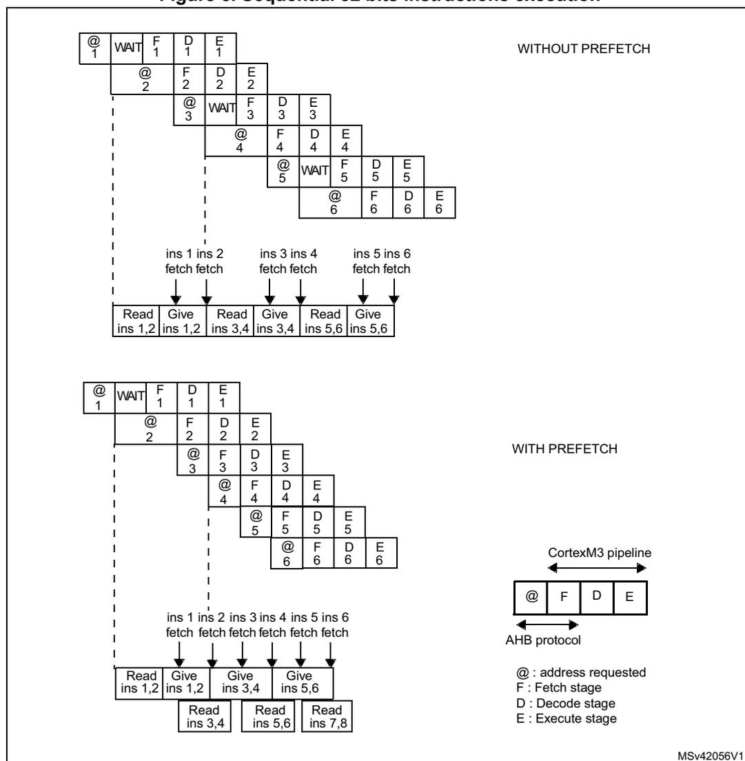
Each Flash memory read operation provides 64 bits from either 2 instructions of 32 bits or 4 instructions of 16 bits depending on the program launched. So, in case of sequential code, at least 2 CPU cycles are needed to execute the previous read instruction line. Prefetch on the I-Code bus can be used to read the next sequential instruction line from the Flash memory while the current instruction line is being requested by the CPU. Prefetch is enabled by setting the PRFTEN bit in the FLASH_ACR register. This feature is useful if at least one wait state is needed to access the Flash memory.
Figure 5 shows the execution of sequential 32-bit instructions with and without prefetch when 1 WS is needed to access the Flash memory.
Figure 5. Sequential 32 bits instructions execution
WITHOUT PREFETCH
WITH PREFETCH
MSv42056V1
Note: When the code is not sequential (branch), the instruction may not be present neither in the current instruction line used nor in the prefetched instruction line. In this case, the penalty in terms of number of cycles is at least equal to the number of Wait States.
Table 14 shows the supported ACC64, LATENCY and PRFTEN configurations.
Table 14. Allowed configuration in FLASH_ACR
| LATENCY | ACC64 = 0 | ACC64 = 1 | ||
|---|---|---|---|---|
| PRFTEN = 0 | PRFTEN = 1 | PRFTEN = 0 | PRFTEN = 1 | |
| 0 | Yes | No | Yes | Yes |
| 1 | No | No | Yes | Yes |
3.3.3 Data management
The literal pools are fetched from the Flash memory through the D-Code bus during the execution stage of the CPU pipeline. The CPU pipeline is consequently stalled until a requested literal pool is provided. To limit the time lost due to literal pools, accesses through the D-Code AHB data bus have the priority over accesses through the I-Code AHB instruction bus.
3.4 Memory operations
3.4.1 Unlocking/locking memory
The following blocks can be separately locked or unlocked:
- • Data EEPROM with the PECR register
- • Program memory
- • Option bytes
The steps required for each operation are described in the sections below:
Unlocking the Data EEPROM block and the FLASH_PECR register
After reset, Data EEPROM block and the Program/erase control register (FLASH_PECR) are not accessible in write mode and the PELOCK bit in FLASH_PECR is set. The same unlocking sequence unprotects them both at the same time.
The following sequence is used to unlock the Data EEPROM block and FLASH_PECR register:
- • Write PEKEY1= 0x89ABCDEF to the Program/erase key register (FLASH_PEKEYR)
- • Write PEKEY2= 0x02030405 to the Program/erase key register (FLASH_PEKEYR)
Any wrong key sequence locks up the Data EEPROM block and the FLASH_PECR register until the next reset, and return a bus error (Cortex ® -M3 hardfault or busfault). So a bus error is returned in any of the three cases below:
- • after the first write access if the entered PEKEY1 value is erroneous
- • during the second write access if PEKEY1 is correctly entered but the PEKEY2 value does not match
- • if there is any attempt to write a third value to PEKEYR
When properly executed, the unlocking sequence clears the PELOCK bit in the FLASH_PECR register.
To lock the FLASH_PECR and the data EEPROM again, the software only needs to set the PELOCK bit in FLASH_PECR.
Unlocking the program memory
An additional protection is implemented to write to the program memory (in pages not write-protected (WRP)).
After reset, the program memory is not accessible in write mode: the PRGLOCK bit is set in FLASH_PECR. Write access to the program memory is granted again by clearing the PRGLOCK bit.
The following sequence is used to unlock the program memory:
- • Unlock the FLASH_PECR register
- • Write PRGKEY1= 0x8C9DAEBF to the Program memory key register (FLASH_PRGKEYR)
- • Write PRGKEY2= 0x13141516 to the Program memory key register (FLASH_PRGKEYR)
Any wrong key sequence locks up PRGLOCK in FLASH_PECR until the next reset, and return a bus error (Cortex ® -M3 hardfault or busfault). So a bus error is returned in any of the three cases below:
- • after the first write access if the entered PRGKEY1 value is erroneous
- • during the second write access if PRGKEY1 is correctly entered but the PRGKEY2 value does not match
- • if there is any attempt to write a third value to PRGKEYR
When properly executed, the unlocking sequence clears the PRGLOCK bit and the program memory is write accessible.
To lock the program memory again, the software only needs to set the PRGLOCK bit in FLASH_PECR.
Unlocking the option byte block
An additional write protection is implemented on the option byte block.
After reset, the option bytes are not accessible in write mode: the OPTLOCK bit in FLASH_PECR is set. Write access to the option bytes is granted again by clearing OPTLOCK.
The following sequence is used to unlock the option byte block:
- • Unlock the FLASH_PECR register
- • Write OPTKEY1= 0xFBEAD9C8 to the Option key register (FLASH_OPTKEYR)
- • Write OPTKEY2= 0x24252627 to the Option key register (FLASH_OPTKEYR)
Any wrong key sequence locks up OPTLOCK in FLASH_PECR until the next reset, and return a bus error (Cortex ® -M3 hardfault or busfault). So a bus error is returned in any of the three cases below:
- • after the first write access if the entered OPTKEY1 value is erroneous
- • during the second write access if OPTKEY1 is correctly entered but the OPTKEY2 value does not match
- • if there is any attempt to write a third value to OPTKEYR
When properly executed, the unlocking sequence clears the OPTLOCK bit and the option bytes are write accessible.
To lock the option byte block again, the software only needs to set the OPTLOCK bit in FLASH_PECR.
3.4.2 Erasing memory
Different erase operations are available for Program memory and Data EEPROM because they have different granularity. These operations are:
- • Word and double word erase: for Data EEPROM
- • Page erase (and parallel page erase for Cat.4, Cat.5 and Cat.6 devices): for Program memory
- • Mass erase: this erases the Program memory, Data EEPROM and Option bytes (in both banks for Cat.4, Cat.5 and Cat.6 devices)
Data EEPROM word erase
This operation is used to erase a word in Data EEPROM. To do so:
- • Unlock the Data EEPROM and the FLASH_PECR register
- • Write a word to a valid address in data EEPROM with the value 0x0000 0000
- • This activates an erase phase
Note: This function can be executed from both banks, RAM or external memory. If it is from the same bank, the program is stalled for one Tprog.
Data EEPROM double word erase
This operation is used to erase a double word in Data EEPROM.
To do so:
- • Unlock the Data EEPROM and the FLASH_PECR register
- • Set the ERASE bit in the FLASH_PECR register
- • Set the DATA bit in the FLASH_PECR register to erase a data double word
- • Write 0x0000 0000 to each of the two data words to be erased
- • Wait for the BSY bit to be cleared
Note: This function can be executed from one bank to the other one, or from RAM. In case of a read access in the same bank during this feature, a Bus error is generated.
Warning: Data EEPROM double word erase is possible only from SRAM, from external memory or from bank 1 to bank 2 and vice versa.
Program memory page erase
This operation is used to erase a page in program memory (64 words). To do so:
- • Unlock the FLASH_PECR register
- • Unlock the Program memory
- • Set the ERASE bit in the FLASH_PECR register
- • Set the PROG bit in the FLASH_PECR register to choose program page
- • Write 0x0000 0000 to the first word of the program page to erase
- • Wait for the BSY bit to be cleared
Note: This function can be executed from both banks, RAM or external memory. If it is from the same bank, the program is stalled for one Tprog.
Program memory parallel page erase
This operation is available for Cat.4, Cat.5 and Cat.6 devices only. It is used to erase two parallel pages in program memory (64 words in each bank). To do so:
- • Unlock the FLASH_PECR register
- • Unlock the Program memory
- • Set the PARALLBANK bit in the FLASH_PECR register
- • Set the ERASE bit in the FLASH_PECR register
- • Set the PROG bit in the FLASH_PECR register to choose program page
- • Write 0x0000 0000 to the first word of the program page to erase in the first bank and 0x0000 0000 to the first word of the program page to erase in the second bank.
- • Wait for the BSY bit to be cleared
Note: This function can be executed only from RAM or external memory.
3.4.3 Programming memory
Program memory Fast Word Write
This operation is used to write a word to the program memory, assuming that it was previously erased. To do so:
- • Unlock the FLASH_PECR register
- • Unlock the Program memory
- • Write a word to a valid address in the program memory. This activates a programming phase
Note: This function can be executed from both Banks, Ram or external memory. If it is from the same bank the program is stalled for one Tprog.
Program memory Half Page Write
This operation is used to write half a page to the program memory (32 words). To do so:
- • Unlock the FLASH_PECR register
- • Unlock the program memory
- • Set the FPRG bit in the FLASH_PECR register (this configures FLASH_PECR to perform a data buffer loading sequence)
- • Set the PROG bit in the FLASH_PECR register to access the required program memory page
- • Wait for the BSY bit to be cleared
- • Directly write half a page with 32 different words to the program memory address space. The words must be written sequentially starting from word 0 and ending with word 31
Warning: Half Page Write is possible only from SRAM, from external memory or from bank 1 to bank 2 and vice versa.
- Note:
- 1 If there are more than 32 words to write, after 32 words another Half Page programming operation starts and has to be finished before any other access to NVM occurs.
- 2 In case of a read access in the same bank during this feature, a bus error is generated.
Program memory Parallel Half Page Write
This operation is used to write two half pages to the program memory (32 words in each bank). This operation is available for Cat.4, Cat.5 and Cat.6 devices only.
- • Unlock the FLASH_PECR register
- • Unlock the program memory
- • Set the PARALL_BANK bit in the FLASH_PECR register to configure FLASH_PECR to perform parallel loading of 2 sequences of 32 words, one in each bank
- • Set the FPRG bit in the FLASH_PECR register (this configures FLASH_PECR to perform the data buffer loading sequences)
- • Set the PROG bit in the FLASH_PECR register to access the required program memory page
- • Wait for the BSY bit to be cleared
- • Write two half pages directly with 64 different words to the program memory address space, 32 words in each bank. 32 words must be written sequentially starting with word 0 and ending with word 31 in bank 1. Then, in bank 2, 32 words must be written sequentially starting with word 32 and ending with word 63.
Note: This function can be executed only from RAM or external memory. Read access to EEprom during this function is forbidden.
Data EEPROM double Word Write
This operation is used to write a double word to the data EEPROM. To do so:
- • Unlock the Data EEPROM and the FLASH_PECR register
- • Set the FPRG bit in the FLASH_PECR register (this configures FLASH_PECR to perform a data buffer loading sequence)
- • Set the DATA bit in the FLASH_PECR register to access the required data EEPROM page
- • Wait for the BSY bit to be cleared
- • Directly write a double word by writing 2 words to the data EEPROM address space. The words must be written sequentially starting from word 0 and ending with word 1.
Warning: Data EEPROM double word write is possible only from SRAM, from external memory or from bank 1 to bank 2 and vice versa.
- Note:
- 1 A data EEPROM double word is written to the data EEPROM only if the first address to load is the start address of a double word (multiple of double word).
- 2 In case of a read access in the same bank during this feature, a bus error is generated.
Data EEPROM Fast Word Write
This operation is used to write a word to the data EEPROM assuming that it was previously erased. The time taken for this operation is 1 tprog (see Table 20 on page 77 for more details).
- • Unlock the Data EEPROM and the FLASH_PECR register
- • Clear the FTDW bit (FLASH_PECR[8]) assuming that the word is already erased (0x00000000).
- • Write a word to a valid address in the data EEPROM
- • The following operations are then performed automatically by the Flash memory interface:
- – The Flash memory interface addresses and reads the word to be written to
- – A ECC is calculated for the new word to write to the memory
- – A write operation is immediately executed (the word read by the interface must be 0x00000000 and the FTDW bit must be cleared)
Note: This function can be executed from any memory. If it is from the same bank the program is stalled for one Tprog.
Data EEPROM Word Write
This operation is used to write a word to the data EEPROM whatever the previous value of the word to be written to. The time taken for this is 1 or 2 tprog, depending on the FTDW bit (see Table 20 on page 77 for more details).
- • Unlock the Data EEPROM and the FLASH_PECR register
- • Configure (Set/Clear) the FTDW bit (FLASH_PECR[8]) to execute Word Write, whatever the previous value of the word be written to
- • Write a word to a valid address in the data EEPROM
- • The following operations are then performed automatically by the Flash memory interface:
- – The Flash memory interface addresses and reads the word to be written to
- – A new ECC is calculated for the new word to write to the memory
- – Case 1: FTDW bit = 0:
If the word read by the interface was not 0x00000000, an erase operation is done automatically followed with a write operation. The time taken for this is 2 tprog.
If the word read by the interface was 0x00000000, a write operation is immediately executed (it takes the same time as Fast Word Write, 1 tprog). - – Case 2: FTDW bit = 1:
If the FTDW bit is set, an erase operation is always done automatically followed by a write operation. The time taken for this is 2 tprog.
Note: This function can be executed from any memory. If it is from the same bank the program is stalled for one Tprog.
Data EEPROM Fast Half Word Write
This operation is used to write a NON NULL (a) half word to the data EEPROM assuming that the complete word was previously erased. The time taken for this is 1 tprog (see Table 20 on page 77 for more details).
- • Unlock the Data EEPROM and the FLASH_PECR register
- • Clear the FTDW bit (FLASH_PECR[8]) assuming that the word is already erased (0x00000000)
- • Write a half word to a valid address in the data EEPROM
- • The following operations are then performed automatically by the Flash memory interface:
- – The Flash memory interface addresses and reads the word to be written to
- – A ECC is calculated for the new half word to write to the memory
- – A write operation is immediately executed (the word read by the interface must be 0x00000000 and the FTDW bit must be cleared)
Note: This function can be executed from any memory. If it is from the same bank the program is stalled for one Tprog.
Data EEPROM Half Word Write
This operation is used to write a NON NULL (a) half word to the data EEPROM whatever the previous value of the word to be written to. The time taken for this is 1 or 2 tprog, depending on the FTDW bit (see Table 20 on page 77 for more details).
- • Unlock the Data EEPROM and the FLASH_PECR register
- • Configure (Set/Clear) the FTDW bit (FLASH_PECR[8]) to execute half Word Write, whatever the previous value of the half word to be written to
- • Write a half word to a valid address in the data EEPROM
- • The following operations are then performed automatically by the Flash memory interface:
- – The Flash memory interface addresses and reads the word to be written to
- – A new ECC is calculated for the new half word to write to the memory
- – Case 1: FTDW bit = 0:
If the word read by the interface was not 0x00000000, an erase operation is done automatically followed by a write operation. The time taken for this is 2 tprog.
If the word read by the interface was 0x00000000, a write operation is immediately executed (it takes the same time as Fast half word Write, 1 tprog). - – Case 2: FTDW bit = 1:
An erase operation is always done automatically followed by a write operation. The time taken for this is 2 tprog.
Note: This function can be executed from any memory. If it is from the same bank the program is stalled for one Tprog.
a. This restriction applies only for Cat.1 devices.
Data EEPROM Fast Byte Write
This operation is used to write a NON NULL (a) Byte to the data EEPROM assuming that the complete word was previously erased. The time taken for this is 1 tprog (see Table 20 on page 77 for more details).
- • Unlock the Data EEPROM and the FLASH_PECR register
- • Clear the FTDW bit (FLASH_PECR[8]) assuming that the word is already erased (0x00000000).
- • Write a byte to a valid address in the data EEPROM
- • The following operations are then performed automatically by the Flash memory interface:
- – The Flash memory interface addresses and reads the word to be written to
- – A new ECC is calculated for the new byte to write to the memory
- – A write operation is immediately executed (the word read by the interface must be 0x00000000 and the FTDW bit must be cleared)
Note: This function can be executed from any memory. If it is from the same bank, the program is stalled for one Tprog.
Data EEPROM Byte Write
This operation is used to write a NON NULL (1) byte to the data EEPROM whatever the previous value of the word to be written to. The time taken for this is 1 or 2 tprog, depending on the FTDW bit (see Table 20 on page 77 for more details).
- • Unlock the Data EEPROM and the FLASH_PECR register
- • Configure (Set/Clear) the FTDW bit (FLASH_PECR[8]) to execute byte Write, whatever the previous value of the word to write to
- • Write a NON NULL byte to a valid address in the data EEPROM
- • The following operations are then performed automatically by the Flash memory interface:
- – The Flash memory interface addresses and reads the word to be written to
- – A new ECC is calculated for the new byte to write to the memory
- – Case 1: FTDW bit = 0:
If the word read by the interface was not 0x00000000, an erase operation is done automatically followed by a write operation. The time taken for this is 2 tprog.
If the word read by the interface was 0x00000000, a write operation is immediately executed (it takes the same time as Fast byte Write, 1 tprog). - – Case 2: FTDW bit = 1:
An erase operation is always done automatically followed by a write operation. The time taken for this is 2 tprog.
Note: This function can be executed from any memory. If it is from the same bank, the program is stalled for one Tprog.
a. This restriction applies only for Cat.1 devices.
Table 15. Data EEPROM programming times
| - | FTDW bit | Word erase state | Programming time | Comments |
|---|---|---|---|---|
| Data EEPROM Fast Word/Half Word/Byte Write | 0 | Word previously erased | 1 Tprog | User software has already erased the selected word using the Data EEPROM double word/word erase |
| Data EEPROM Word/Half Word/Byte Write | 0 | Word previously erased | 1 Tprog | The word read by the interface is 0x0 ==> no need for erase, this case is equal to Fast Word/Half Word/Byte write |
| 0 | Word not erased | 2 Tprog | The word read by the interface is not 0x0 ==> an erase is done automatically | |
| 1 | Word previously erased or word not erased | 2 Tprog | An erase is done automatically whatever the word read by the interface (ECC module) |
- Note:
- 1 When programming a Data Word, Data Half-word or Data byte from Program memory, the DCode and ICode are locked for a duration of 1 to 3 tprog. After the end of programming, the code execution resumes. To avoid this behavior, the write operation has to be executed from SRAM, the other bank, or external memory.
- 2 When programming Data Word or Data Half-word at non-aligned addresses, the write operation may take more than 1 tprog time.
- 3 During the Program memory half page write, Data EEPROM double word erase and Data EEPROM double word write, all read operations on the written bank are forbidden (this includes DMA read operations and debugger read operations such as breakpoints, periodic updates, etc.)
- 4 If a PGAERR is set during a Program memory half page write or Data EEPROM double word write, the complete write operation is aborted. Software should then reset the FPRG and PROG/DATA bits and restart the write operation from the beginning.
3.4.4 Read while write (RWW)
In Cat.4, Cat.5 and Cat.6 devices, the Flash module is composed of 2 banks. These 2 banks are identical. They each contain:
- • Program memory (up to 256 Kbytes)
- • Data EEPROM memory (up to 8 Kbytes)
- • Information block (System memory (4 Kbytes), and option bytes)
This architecture makes it possible to:
- • Read bank 1 and write bank 2 (program or data matrix)
- • Read bank 2 and write bank 1 (program or data matrix)
- • Read bank 1 and read bank 2
- • Write bank 1 and write bank 2 with some restrictions:
- – during Mass Erase
- – during Parallel Half Page Write
- – during Parallel Page Erase
All other Write while write features can't occur exactly in same time but they are managed by memory interface:
- • when a write access in one bank occurs when the other bank is being written, the bus is stalled until the end of the first programming and the second one can be executed.
- • when a write access in one bank occurs when the other bank is performing a multiple write access, a WRPERR is set and the new write request is aborted.
In the same way, read access and a write access can't occur exactly in same time, but they are managed by memory interface:
- • when a read access in one bank occurs when this bank is being written, the bus is stalled until the end of the programming and then the read can be executed.
- • when a read access in one bank occurs when this bank is being written during a multiple write access, a BUS ERROR is returned.
Caution: It is prohibited to perform multiple programming in one bank (HalfPage, DoubleWord from one bank to the same bank).
Table 16. Read While Write Summary
| Execution from | Operation | Destination | Comment |
|---|---|---|---|
| PROG 1 (BANK 1) | WordErase FastByteWrite FastHalfWordWrite ByteWrite HalfWordWrite | DATA2 (RWW) DATA1(with Tprog penalty) | - |
| FastWordWrite WordWrite | DATA2 (RWW) PROG 2 (RWW) DATA1 (with Tprog penalty) PROG 1 (with Tprog penalty) | ||
| PageErase | PROG 2 (RWW) PROG 1 (with Tprog penalty) | ||
| DoubleWordErase DoubleWordWrite | DATA2 (RWW) DATA 1( prohibited ) | a new write access to DATA1 or PROG 1 => WRPERR a read access to BANK 2 => HARD FAULT (bus error) | |
| HalfPageWrite | PROG2 (RWW) PROG1 ( prohibited ) |
Table 16. Read While Write Summary (continued)
| Execution from | Operation | Destination | Comment |
|---|---|---|---|
| PROG 2 (BANK 2) | WordErase FastByteWrite FastHalfWordWrite ByteWrite HalfWordWrite | DATA1 (RWW) DATA2(with Tprog penalty) | - |
| FastWordWrite WordWrite | DATA1 (RWW) PROG 1(RWW) DATA 2 (with Tprog penalty) PROG 2 (with Tprog penalty) | ||
| PageErase | PROG 1 (RWW) PROG 2 (with Tprog penalty) | ||
| DoubleWordErase DoubleWordWrite | DATA 1 (RWW) DATA 2 ( prohibited ) | ||
| HalfPageWrite | PROG 1 (RWW) PROG 2 ( prohibited ) | ||
| RAM and external memory | all operations including: ParallPageErase ParallHalfPageWrite MassErase | PROG 1 DATA 1 PROG 2 DATA 2 | - |
Alignment error flag
The Flash memory interface checks three kinds of alignment:
- • A half page is written to the program memory only if the first address to load is the start address of a half page (multiple of 128 bytes) and the 31 remaining words to load are in the same half page.
- • A double word is written to the data EEPROM only if the first address to load is the start address of a double word (multiple of 8 bytes)
- • Change of page is not possible during half page programming
If the alignment check is not correct, the PGAERR flag (FLASH_SR[8]) is set and an interrupt can be generated. The programming operation aborts.
Size error flag
During the write and erase procedures, the Flash memory interface checks the data size to verify the coherence between the size of the data to write and the allowed operations.
Table 17. Prohibited operations
| Memory block | Data size |
|---|---|
| Program memory | Byte/Half-Word Write prohibited Byte/Half-Word/Word Erase prohibited |
| Option byte block | Byte/Half Word prohibited |
If the check is not correct, a flag SIZERR (FLASH_SR[9]) is set and a interrupt can be generated.
Bus error (Cortex ® -M3 hardfault or Busfault)
A bus error (Cortex ® -M3 hardfault or Busfault) is returned in three cases:
- • When read access through D bus or I bus is performed when memory is read protected and while the debug features are connected or boot is executing from SRAM.
- • Wrong DATA EEPROM/FLASH_PECR register/Program memory Bytes unlock sequence. Refer to Section 3.4.1: Unlocking/locking memory for more details.
- • For Cat.4, Cat.5 and Cat.6 devices, when a read access on bank 1 or bank 2 is performed while a DoubleWordErase, DoubleWordWrite or a HalfPageWrite is operating in the same bank.
3.5 Option byte description
Part of the Flash memory module is reserved for the storage of a set of option bytes. These option bytes contain information on the configuration of the product and they are configured according to the end application requirements. As a configuration example, you can select the watchdog in hardware or software mode.
In the option byte block, a 32-bit word is mapped as shown in the table below.
| 31 | 30 | 29 | 28 | 27 | 26 | 25 | 24 | 23 | 22 | 21 | 20 | 19 | 18 | 17 | 16 | 15 | 14 | 13 | 12 | 11 | 10 | 9 | 8 | 7 | 6 | 5 | 4 | 3 | 2 | 1 | 0 |
|---|---|---|---|---|---|---|---|---|---|---|---|---|---|---|---|---|---|---|---|---|---|---|---|---|---|---|---|---|---|---|---|
| Complemented option byte1 | Complemented option byte0 | Option byte 1 | Option byte 0 | ||||||||||||||||||||||||||||
The organization of the bytes inside the option block is as shown in Table 18 .
Table 18. Option byte organization
| Address | [31:24] | [23:16] | [15:8] | [7:0] |
|---|---|---|---|---|
| 0x1FF80000 | nSPRMOD[0:0] | nRDP | SPRMOD[0:0] | RDP |
| 0x1FF80004 | 0xFF | nUSER | 0x00 | USER |
| 0x1FF80008 | nWRP1[15:8] | nWRP1[7:0] | WRP1[15:8] | WRP1[7:0] |
| 0x1FF8000C | nWRP1[31:24] | nWRP1[23:16] | WRP1[31:24] | WRP1[23:16] |
| 0x1FF80010 | nWRP2[15:8] | nWRP2[7:0] | WRP2[15:8] | WRP2[7:0] |
| 0x1FF80014 | nWRP2[31:24] | nWRP2[23:16] | WRP2[31:24] | WRP2[23:16] |
| 0x1FF80018 | nWRP3[15:8] | nWRP3[7:0] | WRP3[15:8] | WRP3[7:0] |
| 0x1FF8001C | nWRP3[31:24] | nWRP3[23:16] | WRP3[31:24] | WRP3[23:16] |
| 0x1FF80080 | nWRP4[15:8] | nWRP4[7:0] | WRP4[15:8] | WRP4[7:0] |
| 0x1FF80084 | nWRP4[31:24] | nWRP4[23:16] | WRP4[31:24] | WRP4[23:16] |
Option byte loading is performed in two cases:
- • When OBL_LAUNCH is set (in this case, a reset is generated)
- • After every power-up of the V 18 domain (that is after POR or after Standby)
The option byte loader (OBL) reads the information block and stores the data into the option byte register (FLASH_OBR).
During the option byte loading process, it is possible to check that the loading operation was successful by verifying an option byte and its complement.
If the verification fails, the OPTVERR status bit is set and an interrupt is generated if ERRIE is set. OPTVERRUSR bit is also set in case of a verification error is in USER/nUSER byte.
The option byte registers are accessible in read mode by the CPU.
Table 19. Description of the option bytes
| Memory address | Option bytes |
|---|---|
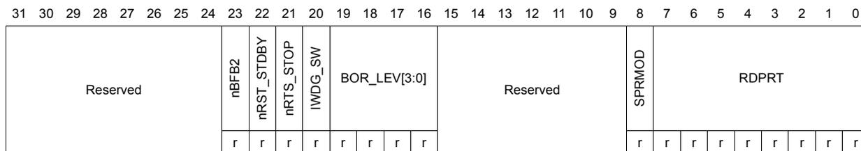
| 0x1FF8 0000 | Bits [31:25]: reserved must be set to 1 Bit 24: nSPRMOD Bits [23:16]: nRDP Bits [15:9]: reserved must be reset to 0 Bit 8: SPRMOD : sector protection mode selection
See Section 3.7.4: PCROP for details. Bits [7:0]: RDP : Read protection option byte (stored in FLASH_OBR[22:16]) The read protection is used to protect the software code stored in Flash memory. 0xAA: Level 0, no protection 0xCC: Level 2, chip protection (debug and boot in SRAM features disabled) Others: Level 1, read protection of memories (debug features limited) |
| 0x1FF8 0004 | Bits [23:16] nUSER Bits [7:0] USER : User option byte (stored in FLASH_OBR[23:16]) This byte is used to configure the following features:
Bits 3:0: BOR_LEV[3:0] : Brownout reset threshold level Bit 4: IWDG_SW
Bit 5: nRST_STOP
Bit 6: nRST_STDBY
Bit 7: nBFB2 This bit is available for Cat.4, Cat.5 and Cat.6 devices only. This bit is used to select the boot space between Flash Bank2/Bank1 and another boot sources. 0: If pins BOOT1 = 0 and BOOT0 = x, the system bootloader is started after reset (boot from system memory), and checks in the following order:
1: Boot space is selected by BOOT0 and BOOT1 pins (see Table 6: Boot modes ). |
Table 19. Description of the option bytes (continued)
| Memory address | Option bytes |
|---|---|
| 0x1FF8 0008 | WRP1
: Memory write protection option bytes Bits [31:16]: nWRP1[15:0] Bits [15:0]: WRP1[15:0] are stored in FLASH_WRPR1[15:0]) 0: Write protection not active on selected sector 1: Write protection active on selected sector |
| 0x1FF8 000C | WRP1
: Memory write protection option bytes Bits [31:16]: nWRP1[31:16] Bits [15:0]: WRP1[31:16] are stored in FLASH_WRPR1[31:16]) 0: Write protection not active on selected sector 1: Write protection active on selected sector |
| 0x1FF8 0010 | WRP2
(1)
: Memory write protection option bytes Bits [31:16]: nWRP2[15:0] Bits [15:0]: WRP2[15:0] are stored in FLASH_WRPR2[15:0]) 0: Write protection not active on selected sector 1: Write protection active on selected sector |
| 0x1FF8 0014 | WRP2
(1)
: Memory write protection option bytes Bits [31:16]: nWRP2[31:16] Bits [15:0]: WRP2[31:16] are stored in FLASH_WRPR2[31:16]) 0: Write protection not active on selected sector 1: Write protection active on selected sector |
| 0x1FF8 0018 | WRP3
(2)
: Memory write protection option bytes Bits [31:16]: nWRP3[15:0] Bits [15:0]: WRP3[15:0] are stored in FLASH_WRPR3[15:0]) 0: Write protection not active on selected sector 1: Write protection active on selected sector |
| 0x1FF8 001C | WRP3
(2)
: Memory write protection option bytes Bits [31:16]: nWRP3[31:16] Bits [15:0]: WRP3[31:16] are stored in FLASH_WRPR3[31:16]) 0: Write protection not active on selected sector 1: Write protection active on selected sector |
| 0x1FF8 0080 | WRP4
(3)
: Memory write protection option bytes Bits [31:16]: nWRP4[15:0] Bits [15:0]: WRP4[15:0] are stored in FLASH_WRPR4[15:0]) 0: Write protection not active on selected sector 1: Write protection active on selected sector |
| 0x1FF8 0084 | WRP4
(3)
: Memory write protection option bytes Bits [31:16]: nWRP4[31:16] Bits [15:0]: WRP4[31:16] are stored in FLASH_WRPR4[31:16]) 0: Write protection not active on selected sector 1: Write protection active on selected sector |
1. WRP2 is available in Cat.3, Cat.4, Cat.5 and Cat.6 devices.
2. WRP3 is available in Cat.4, Cat.5 and Cat.6 devices only.
3. WRP4 is available in Cat.5 devices only.
3.5.1 Option byte block programming
Only Fast Word Write, Word Write and Word Erase are possible in the option byte block.
The option bytes are not programmed in the same way as program/data EEPROM addresses.
Two unlock sequences are required:
- • Unlock the FLASH_PECR register
- • Unlock the option byte block
To modify the option bytes, the following steps are mandatory:
- • The two option bytes of a given word must be written at the same time.
- • The two complementary option bytes of a given word must be calculated and written at the same time (see Section 3.5: Option byte description on page 73 for details on the mapping of the option bytes in a 32-bit word).
- • The user can write to the option bytes to configure them depending on his requirements.
- • To automatically update them in the option byte registers by option byte loading, the OBL_LAUNCH in the FLASH_PECR register should be set and a system reset is generated.
- • Option byte error flags should be cleared to be able to program a new option byte.
The following table summarizes the program and erase functions.
Note: The Option bytes are only loaded when they are already programmed correctly with the corresponding complementary bytes.
3.6 Quick reference to programming/erase functions
Table 20. Programming/erase functions (Cat.1, Cat.2 and Cat.3 devices)
| Operation | Block | Bit/procedure | Time | |
|---|---|---|---|---|
| Erase operation | Word erase (1) | Data EEPROM Option bytes | Write directly the value 0x0000 0000 into the address | 1 tprog |
| Page Erase (2) | Program memory | ERASE = 1 PROG = 1 | 1 tprog | |
| Double Word Erase (3) (4) | Data EEPROM | FPRG = 1 DATA = 1 | 1 tprog | |
| Mass Erase | Program memory + Data EEPROM + Option bytes + backup registers (in RTC) | RDP: level1 -> level0 | 2 tprog for erase + 1 tprog for program |
Table 20. Programming/erase functions (Cat.1, Cat.2 and Cat.3 devices) (continued)
| Operation | Block | Bit/procedure | Time | |
|---|---|---|---|---|
| Write operation | Fast Word Write | Program memory Data EEPROM Option bytes | FTDW = 0 | 1 tprog |
| Word Write (5) | Data EEPROM Option bytes | FTDW = 1 or 0 | 1 or 2 tprog | |
| Half Page Write (3) (6) | Program memory | FPRG = 1 PROG = 1 | 1 tprog | |
| Double Word Write (3)(4) | Data EEPROM | FPRG = 1 DATA = 1 | 1 tprog | |
| Fast Byte Write
(7) Fast Half Word Write (7)(5) | Data EEPROM | FTDW = 0 | 1 tprog | |
| Byte Write
(7) Half Word Write (7)(5) | Data EEPROM | FTDW = 1 or 0 | 1 or 2 tprog |
- 1. A data EEPROM word is erased in the data EEPROM only if the address to load is the start address of a word (multiple of a word).
- 2. A Page is erased in the Program memory only if the address to load is the start address of a page (multiple of 256 bytes).
- 3. The Half Page Write, Double Word Erase and Double Word Write are possible only from SRAM, alternate bank or external memory.
- 4. A data EEPROM double word is written or erased to the data EEPROM only if the first address to load is the start address of a double word (multiple of double word).
- 5. When programming Data Word or Data Half-word at non-aligned addresses, the write operation may take more than 1 tprog time.
- 6. A half page is written to the program memory only if the first address to load is the start address of a half page (multiple of 128 bytes).
- 7. The Fast Byte Write, Fast Half Word Write, Byte Write and Half Word Write can be used only to write a NON NULL byte/half word.
Note: Programming/erasing of NVM memories is possible only if the internal voltage regulator is in Range1 and Range2).
Table 21. Programming/erase functions (Cat.4, Cat.5 and Cat.6 devices)
| Operation | Block | Bit/procedure | Time | |
|---|---|---|---|---|
| Erase operation | Word erase (1) | Data EEPROM Option bytes | Write directly the value 0x0000 0000 into the address | 1 tprog |
| Page Erase (2) | Program memory | ERASE = 1 PROG = 1 | 1 tprog | |
| ParallPageErase | Program memory | ERASE = 1 PROG = 1 PARALLBANK = 1 | 1 tprog | |
| Double Word Erase (3) (4) | Data EEPROM | FPRG = 1 DATA = 1 | 1 tprog | |
| Mass Erase | Program memory +Data EEPROM + Option bytes + backup registers (in RTC) | RDP: level1 -> level0 | 2 tprog for erase + 1 tprog for program | |
| Write operation | Fast Word Write | Program memory Data EEPROM Option bytes | FTDW = 0 | 1 tprog |
| Word Write (5) | Data EEPROM Option bytes | FTDW = 1 or 0 | 1 or 2 tprog | |
| Half Page Write (3) (6) | Program memory | FPRG = 1 PROG = 1 | 1 tprog | |
| ParallHalfPageWrite | Program memory | FPRG = 1 PARALLBANK = 1 PROG = 1 | 1 tprog | |
| Double Word Write (3)(4) | Data EEPROM | FPRG = 1 DATA = 1 | 1 tprog | |
| Fast Byte Write
(7) Fast Half Word Write (7)(5) | Data EEPROM | FTDW = 0 | 1 tprog | |
| Byte Write
(7) Half Word Write (7)(5) | Data EEPROM | FTDW = 1 or 0 | 1 or 2 tprog |
1. A data EEPROM word is erased in the data EEPROM only if the address to load is the start address of a word (multiple of a word).
2. A Page is erased in the Program memory only if the address to load is the start address of a page (multiple of 256 bytes).
3. The Half Page Write, Double Word Erase and Double Word Write are possible only from SRAM or external memory.
4. A data EEPROM double word is written or erased to the data EEPROM only if the first address to load is the start address of a double word (multiple of double word).
5. When programming Data Word or Data Half-word at non-aligned addresses, the write operation may take more than 1 tprog time.
6. A half page is written to the program memory only if the first address to load is the start address of a half page (multiple of 128 bytes).
- 7. In contrast to Cat.1 devices, in Cat.2, Cat.3, Cat.4, Cat.5 and Cat.6 devices the Fast Byte Write, Fast Half Word Write, Byte Write and Half Word Write can be used to write a NULL byte/half word.
Note: Programming/erasing of NVM memories is possible only if the internal voltage regulator is in Range1 and Range2).
3.7 Memory protection
The Flash memory module can be protected against read accesses.
The memory sectors can also be individually protected against unwanted write accesses caused by loss of program counter contexts.
3.7.1 Readout protection (RDP) of the program and data EEPROMs
The user area of the Flash memory module (data and program) can be protected against read operations. Three read protection levels are defined:
- • Level 0: no read protection
When the read protection level is set to Level 0 by writing 0xAA to the read protection option byte, RDP, all read/write operations (if no write protection is set) from/to the Flash memory module or the backup SRAM are possible in all boot configurations (debug, boot from ram or system memory selected).
Level 1: memory read protection enabled
This is the default read protection level after option byte erase. Read protection Level 1 is activated by writing any value (except for 0xAA and 0xCC used to set Level 0 and level 2, respectively) to the RDP option byte. When read protection Level 1 is set:
- – No Flash memory module access (read, erase, program) is performed while the debug features are connected or boot from RAM or system memory is selected. A bus error (Cortex®-M3 hardfault or Busfault) is generated in case of a Flash memory read request. All operations are possible when Flash user boot is used.
- – Programming the protection option byte to lower protection causes the Flash memory module and the backup registers (in RTC) to be mass-erased. That is, the user code contents are cleared before the read protection is removed.
Note: When Level 1 is active and Level 0 is requested, the following steps are executed:
- – Mass Erase is generated (RDP byte is erased (0x0) and Level 1 is still active and no more code could be executed)".
- – If the OBL Launch is set or Power On Reset (POR) is generated the new RDP byte is loaded (0xAA) and Level 0 is active.
Note: Mass Erase is performed only when Level 1 is active and Level 0 is requested. When the protection level is increased (0->1, 1->2, 0->2) there is no Mass Erase.
- – The Flash memory module is also write-protected if the CPU debug features (JTAG or single-wire) are connected or if boot from RAM or system memory is selected.
Level 2: memory read protection enabled and all debug features disabled
Note: Memory read protection Level 2 is an irreversible operation. The level of protection in this case cannot be decreased to level 0 or level 1.
When read protection Level 2 is activated by writing 0xCC to the RDP option byte, all protections provided by Level 1 are active, system memory and all debug features (CPU JTAG and single-wire) are disabled when booting from SRAM or from system memory and user options can no longer be changed.
Note: The JTAG port is permanently disabled in level 2 (acting as a JTAG fuse). Consequently, boundary scan cannot be performed. STMicroelectronics is not able to perform analysis on defective parts on which the level 2 protection has been set.
Figure 6: RDP levels shows how to go from one RDP level to another.
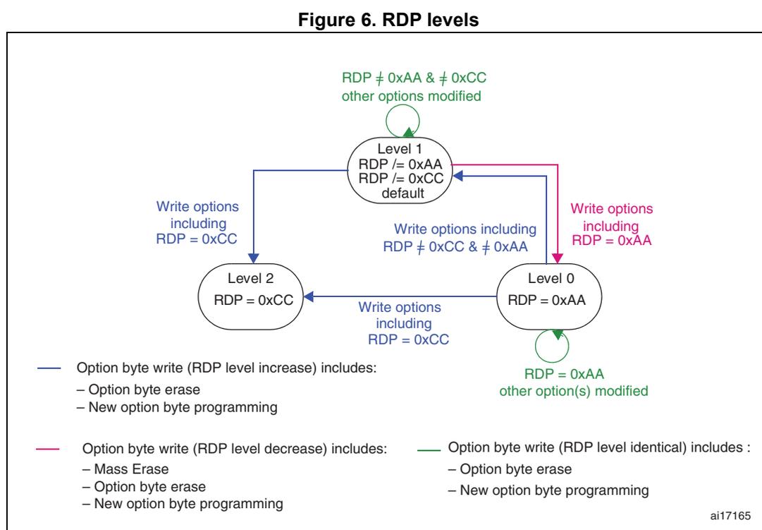
Figure 6. RDP levels
—
Option byte write (RDP level increase) includes:
– Option byte erase
– New option byte programming
—
Option byte write (RDP level decrease) includes:
– Mass Erase
– Option byte erase
– New option byte programming
—
Option byte write (RDP level identical) includes :
– Option byte erase
– New option byte programming
ai17165
The Flash memory module is protected when the RDP option byte and its complement contain the following pair of values:
Table 22. Flash memory module protection according to RDP and its complement
| RDP byte value | RDP's complementary value | Read protection status |
|---|---|---|
| 0xAA | 0x55 | Level 0 |
| Any value except 0xAA or 0xCC | Complement of RDP byte | Level 1 |
| Any value | Not the complement value of RDP | Level 1 |
| 0xCC | 0x33 | Level 2 |
3.7.2 Write protection (WRP) of the program memory
The write protection granularity is the sector (16 pages). This means that 32 option bits are needed to protect 128 Kbyte program memory.
The protection is activated by configuring the WRPx option bytes which are loaded at power-up or reloaded by setting the OBL_LAUNCH bit in the FLASH_PECR register. A copy of these option bits are in the FLASH_WRPRx registers.
Note: When the memory read protection level is selected (RDP level = 1), it is not possible to program or erase the program and data EEPROMs if the CPU debug features are connected (JTAG or Single Wire) or boot from RAM or system memory is selected, even if nWRPx = 0.
The data EEPROM is not protected by WRP bits.
3.7.3 Write protection error flag
If an erase/program operation to a write-protected memory page is launched, the write protection error flag (WRPERR) is set in the FLASH_SR register. This flag is set whenever the software attempts to write to any protected address.
Consequently, the WRPERR flag is set when the software tries to write to:
- • a write protected page
- • a System memory page
- • the Program memory, Data EEPROM or option byte block if they are not unlocked by PEKEY, PRGKEY or OPTKEY
- • the Data EEPROM and Program memory when the RDP option byte is set and the device is in debug mode or is booting from SRAM
- • one bank while a DoubleWordErase, DoubleWordWrite or a HalfPageWrite is performed on the other bank (for Cat.4, Cat.5 and Cat.6 devices)
3.7.4 PCROP
This section is only applicable for Cat.2 and Cat.3 devices (except STM32L100xx product categories - see Table 2 ). See device datasheet for PCROP availability.
The user area of the Flash memory can be protected against Dbus read access. This assuming the native code is compiled accordingly with PcROP option.
A protected sector is accessible for code execution (on ICODE bus only), but cannot be read/written on Dbus (CPU data read or debugger access).
This mode is activated by SPRMOD option bit and WRPx option bytes.
- • SPRMOD = 0 : WRPx control the write protection of respective user sectors.
- • SPRMOD = 1 : WRPx control the read protection (PcROP) of respective user sectors.
Any read access performed through the Dbus triggers RDERR flag error when the target sector is read protected.
Any read protected sector is also write protected and any write access to one of these sectors triggers WRPERR (in same way then WRP protection).
Deactivation of SPRMOD and/or unprotection of user sectors can only occurs when the RDP is changing from level-1 to level-0. When SPRMOD is active, if the user options
modification tries to reset SPRMOD or to deactivate WRPx, the programming is launch but SPRMOD or protected sectors stay unchanged.
Note: Active value of WRPx bits is inverted when PCROP mode is active (SPRMOD =1). if WRPx = '0' then user sector i is Read Protected (PcROP).
3.8 Interrupts
Setting the end of programming interrupt enable bit (EOPIE) in the FLASH_PECR register enables an interrupt generation when an erase or program operation successfully ends. In this case, the end of programming (EOP) bit in the FLASH_SR register is set.
Setting the error interrupt enable bit (ERRIE) in the FLASH_PECR register enables an interrupt generation if an error occurs during a program or erase operation, or during option byte loading. In this case, one of the error flags is set in the FLASH_SR register:
- • RDERR (PCROP read protection error flag)
- • WRPERR (write protection error flag)
- • PGAERR (programming alignment error flag)
- • OPTVERR (option validity error flag)
- • OPTVERRUSR (user option validity error flag)
- • SIZERR (size error flag)
Table 23. Interrupts
| Interrupt event | Event flag | Enable control bit |
|---|---|---|
| End of programming | EOP | EOPIE |
| Error | RDERR WRPERR PGAERR OPTVERR OPTVERRUSR SIZERR | ERRIE |
3.9 Register description
3.9.1 Access control register (FLASH_ACR)
Address offset: 0x00
Reset value: 0x0000 0000
| 31 | 30 | 29 | 28 | 27 | 26 | 25 | 24 | 23 | 22 | 21 | 20 | 19 | 18 | 17 | 16 | 15 | 14 | 13 | 12 | 11 | 10 | 9 | 8 | 7 | 6 | 5 | 4 | 3 | 2 | 1 | 0 |
|---|---|---|---|---|---|---|---|---|---|---|---|---|---|---|---|---|---|---|---|---|---|---|---|---|---|---|---|---|---|---|---|
| Reserved | RUN_PD | SLEEP_PD | ACC64 | PRFTEN | LATENCY | ||||||||||||||||||||||||||
| nw | nw | nw | nw | nw | |||||||||||||||||||||||||||
Bits 31:5 Reserved, must be kept cleared.
Bit 4 RUN_PD : Power saving mode during Run
This bit can be written only when it is unlocked by writing to FLASH_PDKEYR.
This bit determines whether the Flash memory module is in Power down mode or Idle mode when the STM32L1xxxx is in Run mode.
The Flash memory module can be placed in Power down mode only when the code is executed from SRAM).
0: Flash module in Idle mode
1: Flash module in Power down mode
Bit 3 SLEEP_PD : Power saving mode during Sleep
This bit is used to put the Flash memory module in Power down mode or Idle mode when the STM32L1xxxx is in Sleep mode.
0: Flash module in Idle mode
1: Flash module in Power down mode
Bit 2 ACC64 : 64-bit access
This bit is used to read data from the memory 64 bits or 32 bits at a time. 32-bit access is used to decreases the memory consumption. On the contrary, 64-bit access is used to improve the performance. In this case it is useful to enable prefetch.
0: 32-bit access
1: 64-bit access
Note: 32-bit access is a low-power mode. It is used only at low frequencies, that is with 0 wait state of latency and prefetch off.
Note: This bit cannot be written at the same time as the LATENCY and PRFTEN bits.
Bit 1 PRFTEN : Prefetch enable
0: prefetch disabled
1: prefetch enabled
Note: Prefetch can be enabled only when ACC64 is set.
This bit can be set or cleared only if ACC64 is set.
Bit 0 LATENCY : Latency
This bit represents the ratio of the CPU clock period to the memory access time.
0: zero wait state
1: one wait state
Note: Latency can be set only when ACC64 is set.
This bit can be set or cleared only if ACC64 is set.
3.9.2 Program/erase control register (FLASH_PECR)
This register is used to perform all erase and program operations. It is write-accessible only after the good write sequence has been executed in FLASH_PEKEYR.
Address offset: 0x04
Reset value: 0x0000 0007
| 31 | 30 | 29 | 28 | 27 | 26 | 25 | 24 | 23 | 22 | 21 | 20 | 19 | 18 | 17 | 16 | 15 | 14 | 13 | 12 | 11 | 10 | 9 | 8 | 7 | 6 | 5 | 4 | 3 | 2 | 1 | 0 |
|---|---|---|---|---|---|---|---|---|---|---|---|---|---|---|---|---|---|---|---|---|---|---|---|---|---|---|---|---|---|---|---|
| Reserved | OBL_LAUNCH | ERRIE | EOPIE | PARALLELBANK | Reserved | FPRG | ERASE | FTDW | DATA | PROG | OPTLOCK | PRGLOCK | PELOCK | ||||||||||||||||||
| rw 1 | rw | rw | rw | rw | rw | rw | rw | rw | rs | rs | rs | ||||||||||||||||||||
Bits 31:19 Reserved, must be kept cleared.
Bit 18 OBL_LAUNCH : Launch the option byte loading
This bit is set by software to launch the option byte loading. This bit is cleared only when the option byte loading has completed. It cannot be written if OPTLOCK is set.
When this bit is set, a reset is generated.
0: Option byte loading complete
1: Option byte has to be loaded
Bit 17 ERRIE : Error interrupt enable
0: interrupt disabled
1: interrupt enabled
Bit 16 EOPIE : End of programming interrupt enable
0: interrupt disabled
1: interrupt enabled
Bit 15 PARALLBANK : Parallel bank mode.
This bit can be set and cleared by software when no program or erase process is on-going.
When this bit is set, 2 half pages can be programmed or 2 pages can be erased in parallel (the first one in the first bank and the second one in the second bank).
0: Parallel bank mode disabled
1: Parallel bank mode enabled
Note: This bit is available in Cat.4, Cat.5 and Cat.6 devices only.
Bits 14:11 Reserved, must be kept cleared.
Bit 10 FPRG : Half Page/Double Word programming mode
This bit can be written by software when no program or erase process is ongoing.
It is used to enable/disable Half Page Programming to the program memory or Double Word Programming to the data EEPROM.
32 loadings are required to program half a page to the program memory.
2 loadings are required to program a double word to the data EEPROM.
This bit is cleared when PELOCK is set.
0: Half Page/Double Word programming disabled
1: Half Page/Double Word programming enabled
Bit 9 ERASE : Page or Double Word erase mode
This bit can be written by software when no program or erase process is on going.
It is used to enable/disable Page Erase on the program memory or Double Word Erase on the data EEPROM and the option byte block.
This bit is cleared when PELOCK is set.
0: Page or Double Word Erase disabled
1: Page or Double Word Erase enabled
Bit 8 FTDW: Fixed time data write for Byte, Half Word and Word programmingThis bit is writable by software when no program or erase process is ongoing.
This bit is used for the data EEPROM only.
It is cleared when PELOCK is set.
0: Programming of a Byte, Half Word or word is performed without any previous erase operation. This is possible if the word being written to is 0x0000 0000.
1: Before the programming of a Byte, Half Word and word an erase phase is automatically performed. So the time of programming is fixed and lasts two \( t_{prog} \)
Bits 7:5 Reserved, must be kept cleared Bit 4 DATA: Data EEPROM selectionThis bit is writable by software when no program or erase process is ongoing.
This bit has to be set prior to data EEPROM double word erase/programming.
This bit is cleared when PELOCK is set.
0: Data EEPROM not selected
1: Data EEPROM selected
Bit 3 PROG: Program memory selectionThis bit is writable by software when no program or erase process is ongoing.
This bit has to be set to gain write access to the program memory, except in the case of word programming.
This bit is cleared when PELOCK is set.
0: Program memory not selected
1: Program memory selected
Bit 2 OPTLOCK: Option bytes block lockThis bit can only be written to 1. When it is set, it indicates that the option byte block is locked.
It is cleared by hardware after detecting the unlock sequence. In the event of an unsuccessful unlock operation or a third access to OPTKEYR, a bus error (Cortex
®
-M3 hardfault or Busfault) is generated and this bit remains set until the next reset.
This bit is set when PELOCK is set.
0: option unlocked
1: option locked
Bit 1 PRGLOCK: Program memory lockThis bit can only be written to 1. When it is set, it indicates that the program memory cannot be written. It is cleared by hardware after detecting the unlock sequence. In the event of an unsuccessful unlock operation or a third access to PRGKEYR, a bus error (Cortex
®
-M3 hardfault or Busfault) is generated and this bit remains set until the next reset.
This bit is set when PELOCK is set.
0: program memory unlocked
1: program memory locked
Bit 0 PELOCK: FLASH_PECR and data EEPROM lockThis bit can only be written to 1. When it is set, it indicates that the FLASH_PECR register and data EEPROM are locked. It is cleared by hardware after detecting the unlock sequence. In the event of unsuccessful unlock operation or a third access to PEKEYR, a bus error (Cortex ® -M3 hardfault or Busfault) is generated and this bit remains set until the next reset.
When this bit is cleared, write access to the data EEPROM is allowed.
0: FLASH_PECR is unlocked
1: FLASH_PECR is locked
3.9.3 Power down key register (FLASH_PDKEYR)
The Power down key register is used to unlock the RUN_PD bit in FLASH_ACR.
Address offset: 0x08
Reset value: 0x0000 0000

| 31 | 30 | 29 | 28 | 27 | 26 | 25 | 24 | 23 | 22 | 21 | 20 | 19 | 18 | 17 | 16 | 15 | 14 | 13 | 12 | 11 | 10 | 9 | 8 | 7 | 6 | 5 | 4 | 3 | 2 | 1 | 0 |
| PDKEYR[31:0] | |||||||||||||||||||||||||||||||
| w | w | w | w | w | w | w | w | w | w | w | w | w | w | w | w | w | w | w | w | w | w | w | w | w | w | w | w | w | w | w | w |
Bits 31:0 PDKEYR[31:0] : RUN_PD in FLASH_ACR key
These bits represent the keys used to set the RUN_PD bit in the FLASH_ACR register.
PDKEY1: 0x04152637
PDKEY2: 0xFAFBFCFD
3.9.4 Program/erase key register (FLASH_PEKEYR)
The Program/erase key register is used to allow access to FLASH_PECR and so, to allow program and erase operations in the data EEPROM.
Address offset: 0x0C
Reset value: 0x0000 0000

| 31 | 30 | 29 | 28 | 27 | 26 | 25 | 24 | 23 | 22 | 21 | 20 | 19 | 18 | 17 | 16 | 15 | 14 | 13 | 12 | 11 | 10 | 9 | 8 | 7 | 6 | 5 | 4 | 3 | 2 | 1 | 0 |
| PEKEYR[31:0] | |||||||||||||||||||||||||||||||
| w | w | w | w | w | w | w | w | w | w | w | w | w | w | w | w | w | w | w | w | w | w | w | w | w | w | w | w | w | w | w | w |
Bits 31:0 PEKEYR[31:0] : FLASH_PEC and data EEPROM key
These bits represent the keys to unlock the write access to the FLASH_PECR register and data EEPROM.
PEKEY1: 0x89ABCDEF
PEKEY2: 0x02030405
3.9.5 Program memory key register (FLASH_PRGKEYR)
The Program memory key register is used to allow program and erase operations in the Program memory. It is write accessible only after a correct write sequence has been executed in FLASH_PEKEYR.
Address offset: 0x10
Reset value: 0x0000 0000

| 31 | 30 | 29 | 28 | 27 | 26 | 25 | 24 | 23 | 22 | 21 | 20 | 19 | 18 | 17 | 16 | 15 | 14 | 13 | 12 | 11 | 10 | 9 | 8 | 7 | 6 | 5 | 4 | 3 | 2 | 1 | 0 |
| PRGKEYR[31:0] | |||||||||||||||||||||||||||||||
| w | w | w | w | w | w | w | w | w | w | w | w | w | w | w | w | w | w | w | w | w | w | w | w | w | w | w | w | w | w | w | w |
Bits 31:0 PRGKEYR[31:0] : Program memory key
These bits represent the keys to unlock the program memory.
PRGKEY1: 0x8C9DAEBF
PRGKEY2: 0x13141516
3.9.6 Option byte key register (FLASH_OPTKEYR)
The Option key register is used to allow program and erase operations in the option byte block. It is write accessible only after the good write sequence has been executed in FLASH_PEKEYR.
Address offset: 0x14
Reset value: 0x0000 0000
| 31 | 30 | 29 | 28 | 27 | 26 | 25 | 24 | 23 | 22 | 21 | 20 | 19 | 18 | 17 | 16 | 15 | 14 | 13 | 12 | 11 | 10 | 9 | 8 | 7 | 6 | 5 | 4 | 3 | 2 | 1 | 0 |
|---|---|---|---|---|---|---|---|---|---|---|---|---|---|---|---|---|---|---|---|---|---|---|---|---|---|---|---|---|---|---|---|
| OPTKEYR[31:0] | |||||||||||||||||||||||||||||||
| w | w | w | w | w | w | w | w | w | w | w | w | w | w | w | w | w | w | w | w | w | w | w | w | w | w | w | w | w | w | w | w |
Bits 31:0 OPTKEYR : Option byte key
These bits represent the keys to unlock the write access to the option byte block.
OPTKEY1: 0xFBEAD9C8
OPTKEY2: 0x24252627
3.9.7 Status register (FLASH_SR)
Address offset: 0x18
system reset value: 0b0000 0000 0000 0000 000x x000 0000 0100
| 31 | 30 | 29 | 28 | 27 | 26 | 25 | 24 | 23 | 22 | 21 | 20 | 19 | 18 | 17 | 16 | 15 | 14 | 13 | 12 | 11 | 10 | 9 | 8 | 7 | 6 | 5 | 4 | 3 | 2 | 1 | 0 |
|---|---|---|---|---|---|---|---|---|---|---|---|---|---|---|---|---|---|---|---|---|---|---|---|---|---|---|---|---|---|---|---|
| Reserved | RDERR | OPTVERRUSR | OPTVERR | SIZERR | PGAERR | WRPERR | Reserved | READY | ENDHV | EOP | BSY | ||||||||||||||||||||
| rc_w1 | rc_w1 | rc_w1 | rc_w1 | rc_w1 | rc_w1 | r | r | r | r | ||||||||||||||||||||||
Bits 31:14 Reserved, must be kept cleared.
Bit 13 RDERR : Read protected error
Set by hardware when an address to be read through the Dbus belongs to a read-protected (PCROP) part of the memory.
Cleared by writing 1.
Bit 12 OPTVERRUSR : Option UserValidity Error.
Set by hardware when the option byte USER has an incorrect complement nUSER when loading option bytes into FLASH_OBR register (see Section 3.5: Option byte description ).
Cleared by writing 1.
If user option byte USER/nUSER has not been properly loaded
OPTVERRUSR is set again. Consequently, an interrupt is generated as soon as ERRIE is set.
Note: This bit is available in Cat.3, Cat.4, Cat.5 and Cat.6 devices only.
Bit 11 OPTVERR : Option validity error
Set by hardware when some option byte has an incorrect complement when loading option bytes into FLASH_OBR register (see Section 3.5: Option byte description ).
Cleared by writing 1.
If some option byte has not been properly loaded
OPTVERR is set again. Consequently, an interrupt is generated as soon as ERRIE is set.
Bit 10 SIZERR : Size error
Set by hardware when the size of the data to program is prohibited.
Cleared by writing it to 1.
Bit 9 PGAERR : Programming alignment error
Set by hardware when the data to program cannot be contained in a given half page or double word.
Cleared by writing it to 1.
Bit 8 WRPERR : Write protected error
Set by hardware when an address to be erased/programmed belongs to a write-protected part of the memory.
Cleared by writing it to 1.
Bits 7:4 Reserved, must be kept cleared.
Bit 3 READY : Flash memory module ready after low-power mode
This bit is set and cleared by hardware.
0: Flash memory module is not ready
1: Flash memory module is ready
Bit 2 ENDHV : End of high voltage
This bit is set and cleared by hardware.
0: High voltage still applied during write/erase operations
1: End of high voltage
Bit 1 EOP : End of operation
This bit is set by hardware if the high voltage stops being applied and programming has not been aborted. It is cleared by software (by writing it to 1).
0: No EOP event occurred
1: An EOP event occurred. An interrupt is generated if EOPIE is set
Bit 0 BSY : Write/erase operations in progress
0: Write/erase operation not in progress
1: Write/erase operation in progress
3.9.8 Option byte register (FLASH_OBR)
Address offset: 0x1C
Reset value: depends on RDP and USER option byte, on virgin part initial value is 0x00F800AA.
| 31 | 30 | 29 | 28 | 27 | 26 | 25 | 24 | 23 | 22 | 21 | 20 | 19 | 18 | 17 | 16 | 15 | 14 | 13 | 12 | 11 | 10 | 9 | 8 | 7 | 6 | 5 | 4 | 3 | 2 | 1 | 0 |
|---|---|---|---|---|---|---|---|---|---|---|---|---|---|---|---|---|---|---|---|---|---|---|---|---|---|---|---|---|---|---|---|
| Reserved | nBFB2 | nRST_STDBY | nRTS_STOP | IWDG_SW | BOR_LEV[3:0] | Reserved | SPRMOD | RDPRT | |||||||||||||||||||||||
| r | r | r | r | r | r | r | r | r | r | r | r | r | r | r | r | r | |||||||||||||||
Bits 31:24 Reserved, must be kept cleared.
Bit 23
nBFB2
: Boot from Bank2. This bit contains the user option byte loaded by the OBL. This bit is used to select the boot space between Flash Bank2/Bank1 and another boot sources.
0: System bootloader is started after reset (boot from system memory). Bootloader in next executes checks in following order:
- If content of first word of Bank2 is valid SRAM address then is jumped to Bank2 (boot from Bank2).
- If content of first word of Bank1 is valid SRAM address then is jumped to Bank1 (boot from Bank1).
- Otherwise system bootloader is executed.
1: Boot space is selected by BOOT0 and BOOT1 pins (see
Table 6: Boot modes
).
This bit is read only.
Note: This bit is available in Cat.4, Cat.5 and Cat.6 devices only.
Bits 22:16 User option byte
These bits contain the user option byte loaded by the OBL.
Bit 22: nRST_STDBY
Bit 21: nRST_STOP
Bit 20: IWDG_SW
Bits 19:16: BOR_LEV[3:0] : Brownout reset threshold level
0xxx: BOR OFF : Reset threshold level for the 1.45 V-1.55 V voltage range (power down only)
In this particular case, V DD33 must have been above BOR LEVEL 1 to start the device OBL sequence in order to disable the BOR. The power-down is then monitored by the PDR.
Note: If the BOR is disabled, a ‘grey zone’ exists between 1.65 V and the V PDR threshold (this means that V DD33 may be below the minimum operating voltage (1.65 V) without causing a reset until it crosses the V PDR threshold)
1000: BOR LEVEL 1 : Reset threshold level for 1.69 V-1.8 V voltage range (power on)
1001: BOR LEVEL 2 : Reset threshold level for 1.94 V-2.1 V voltage range (power on)
1010: BOR LEVEL 3 : Reset threshold level for 2.3 V-2.49 V voltage range (power on)
1011: BOR LEVEL 4 : Reset threshold level for 2.54 V-2.74 V voltage range (power on)
1100: BOR LEVEL 5 : Reset threshold level for 2.77 V-3.0 V voltage range (power on)
These bits are read only.
Bits 15:9 Reserved, must be kept cleared.
Bit 8 SPRMOD : Sector protection mode selection
0: WRP[i]=1 bit in FLASH_WRPRx registers defines sector write protection
1: WRP[i]=0 bit in FLASH_WRPRx registers defines sector write and read (PCROP) protection.
See
Section 3.7.4: PCROP
for details.
Bits 7:0 RDPRT[7:0] : Read protection
These bits contain the read protection option level loaded by the OBL.
0xAA: Level 0, read protection not active
0xCC: Level 2, read protection active
Others: Level 1, read protection of memories active. Default configuration after option byte erase.
3.9.9 Write protection register (FLASH_WRPRx)
Address offset: 0x20, 0x80, 0x84, 0x88
Reset value: Depends on content of Option bytes WRPx, on virgin part initial value is 0x0000 0000
| 31 | 30 | 29 | 28 | 27 | 26 | 25 | 24 | 23 | 22 | 21 | 20 | 19 | 18 | 17 | 16 | 15 | 14 | 13 | 12 | 11 | 10 | 9 | 8 | 7 | 6 | 5 | 4 | 3 | 2 | 1 | 0 |
|---|---|---|---|---|---|---|---|---|---|---|---|---|---|---|---|---|---|---|---|---|---|---|---|---|---|---|---|---|---|---|---|
| WRPx[31:0] | |||||||||||||||||||||||||||||||
| x | x | x | x | x | x | x | x | x | x | x | x | x | x | x | x | x | x | x | x | x | x | x | x | x | x | x | x | x | x | x | x |
Bits 31:0 WRPx[n] : Write protection, where n is the number of the concerned memory sector
These bits contain the write protection option loaded by the OBL.
0: sector n not write protected
1: sector n write protected
Note: FLASH_WRPR2 is available in Cat.3, Cat.4, Cat.5 and Cat.6 devices
FLASH_WRPR3 is available in Cat.4, Cat.5 and Cat.6 devices only.
FLASH_WRPR4 is available in Cat.5 devices only.
3.9.10 Register map
Table 24 summarizes the register map and reset values. The reserved memory areas are highlighted in gray in the table.
Table 24. Register map and reset values
| Offset | Register | 31 | 30 | 29 | 28 | 27 | 26 | 25 | 24 | 23 | 22 | 21 | 20 | 19 | 18 | 17 | 16 | 15 | 14 | 13 | 12 | 11 | 10 | 9 | 8 | 7 | 6 | 5 | 4 | 3 | 2 | 1 | 0 |
|---|---|---|---|---|---|---|---|---|---|---|---|---|---|---|---|---|---|---|---|---|---|---|---|---|---|---|---|---|---|---|---|---|---|
| 0x00 | FLASH_ACR | Reserved | RUN_PD | SLEEP_PD | Acc64 | PRFTEN | LATENCY | ||||||||||||||||||||||||||
| Reset value: 0x0000 0000 | 0 | 0 | 0 | 0 | 0 | ||||||||||||||||||||||||||||
Table 24. Register map and reset values (continued)
| Offset | Register | 31 | 30 | 29 | 28 | 27 | 26 | 25 | 24 | 23 | 22 | 21 | 20 | 19 | 18 | 17 | 16 | 15 | 14 | 13 | 12 | 11 | 10 | 9 | 8 | 7 | 6 | 5 | 4 | 3 | 2 | 1 | 0 |
|---|---|---|---|---|---|---|---|---|---|---|---|---|---|---|---|---|---|---|---|---|---|---|---|---|---|---|---|---|---|---|---|---|---|
| 0x04 | FLASH_PECR | Reserved | OBL_launch | ERRIE | EOPIE | PARALLELBANK | Reserved | FPRG | ERASE | FTDW | Reserved | DATA | PRG | OPTLOCK | PRGLOCK | PELOCK | |||||||||||||||||
| Reset value: 0x0000 0007 | 0 | 0 | 0 | 0 | 0 | 0 | 0 | 0 | 0 | 1 | 1 | 1 | |||||||||||||||||||||
| 0x08 | FLASH_PDKEYR | PDKEYR[31:0] | |||||||||||||||||||||||||||||||
| Reset value: 0x0000 0000 | 0 | 0 | 0 | 0 | 0 | 0 | 0 | 0 | 0 | 0 | 0 | 0 | 0 | 0 | 0 | 0 | 0 | 0 | 0 | 0 | 0 | 0 | 0 | 0 | 0 | 0 | 0 | 0 | 0 | 0 | 0 | 0 | |
| 0x0C | FLASH_PEKEYR | PEKEYR[31:0] | |||||||||||||||||||||||||||||||
| Reset value: 0x0000 0000 | 0 | 0 | 0 | 0 | 0 | 0 | 0 | 0 | 0 | 0 | 0 | 0 | 0 | 0 | 0 | 0 | 0 | 0 | 0 | 0 | 0 | 0 | 0 | 0 | 0 | 0 | 0 | 0 | 0 | 0 | 0 | 0 | |
| 0x10 | FLASH_PRGKEYR | PRGKEYR[31:0] | |||||||||||||||||||||||||||||||
| Reset value: 0x0000 0000 | 0 | 0 | 0 | 0 | 0 | 0 | 0 | 0 | 0 | 0 | 0 | 0 | 0 | 0 | 0 | 0 | 0 | 0 | 0 | 0 | 0 | 0 | 0 | 0 | 0 | 0 | 0 | 0 | 0 | 0 | 0 | 0 | |
| 0x14 | FLASH_OPTKEYR | OPTKEYR[31:0] | |||||||||||||||||||||||||||||||
| Reset value: 0x0000 0000 | 0 | 0 | 0 | 0 | 0 | 0 | 0 | 0 | 0 | 0 | 0 | 0 | 0 | 0 | 0 | 0 | 0 | 0 | 0 | 0 | 0 | 0 | 0 | 0 | 0 | 0 | 0 | 0 | 0 | 0 | 0 | 0 | |
| 0x18 | FLASH_SR | Reserved | RDERR | OPTVERRUSR | OPTVERR | SIZVERR | PGAERR | WRPERR | Reserved | READY | ENDHV | EOP | BSY | ||||||||||||||||||||
| Reset value: 0x0000 0004 | 0 | 0 | 0 | 0 | 0 | 0 | 0 | 1 | 0 | 0 | |||||||||||||||||||||||
| 0x1C | FLASH_OBR | Reserved | nBFB2 | nRST_STDBY | nRST_STOP | IWDG_SW | BOR_LEV [3:0] | Reserved | RDPRT[7:0] | ||||||||||||||||||||||||
| Reset value: 0x xxxx xxxx | x | x | x | x | x | x | x | x | x | x | x | x | x | x | x | x | |||||||||||||||||
| 0x20 | FLASH_WRPR1 | WRP1[31:0] | |||||||||||||||||||||||||||||||
| Reset value: 0x xxxx xxxx | x | x | x | x | x | x | x | x | x | x | x | x | x | x | x | x | x | x | x | x | x | x | x | x | x | x | x | x | x | x | x | x | |
| 0x80 | FLASH_WRPR2 | WRP2[31:0] | |||||||||||||||||||||||||||||||
| Reset value: 0x xxxx xxxx | x | x | x | x | x | x | x | x | x | x | x | x | x | x | x | x | x | x | x | x | x | x | x | x | x | x | x | x | x | x | x | x | |
| 0x84 | FLASH_WRPR3 | WRP3[31:0] | |||||||||||||||||||||||||||||||
| Reset value: 0x xxxx xxxx | x | x | x | x | x | x | x | x | x | x | x | x | x | x | x | x | x | x | x | x | x | x | x | x | x | x | x | x | x | x | x | x | |
Table 24. Register map and reset values (continued)
| Offs et | Register | 31 | 30 | 29 | 28 | 27 | 26 | 25 | 24 | 23 | 22 | 21 | 20 | 19 | 18 | 17 | 16 | 15 | 14 | 13 | 12 | 11 | 10 | 9 | 8 | 7 | 6 | 5 | 4 | 3 | 2 | 1 | 0 |
|---|---|---|---|---|---|---|---|---|---|---|---|---|---|---|---|---|---|---|---|---|---|---|---|---|---|---|---|---|---|---|---|---|---|
| 0x88 | FLASH_WRPR4 | WRP4[31:0] | |||||||||||||||||||||||||||||||
| Reset value: 0x xxxx xxxx | x | x | x | x | x | x | x | x | x | x | x | x | x | x | x | x | x | x | x | x | x | x | x | x | x | x | x | x | x | x | x | x | |