2. System architecture and memory overview
2.1 System architecture
The main system consists of a 32-bit multilayer AHB bus matrix that interconnects:
- • Up to five masters:
- – Cortex ® -M3 I-bus, D-bus and S-bus
- – DMA1 and DMA2
- • Up to five slaves:
- – Internal Flash memory ICode
- – Internal Flash memory DCode
- – Internal SRAM
- – AHB to APBx (APB1 or APB2), which connect all the APB peripherals
- – Flexible Static Memory Controller
These are interconnected using the multilayer AHB bus architecture shown in Figure 1 :
Figure 1. System architecture (Cat.1 and Cat.2 devices)
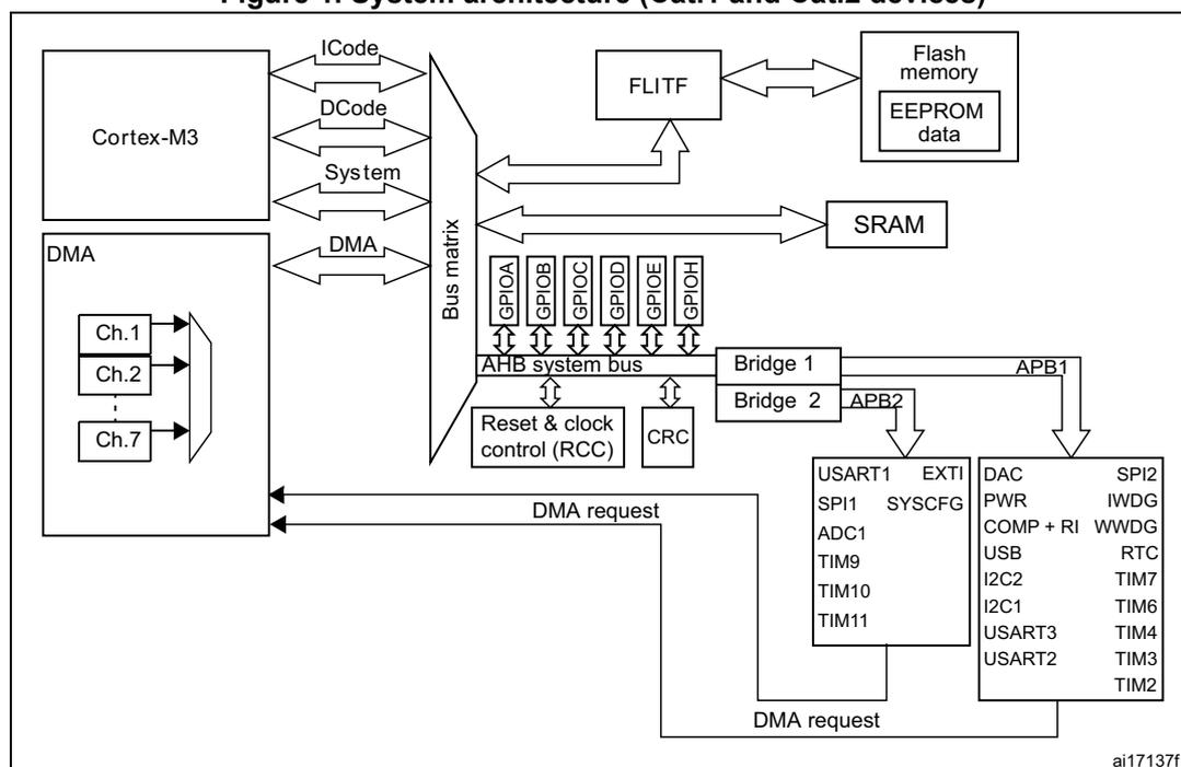
Figure 2. System architecture (Cat.3 devices)
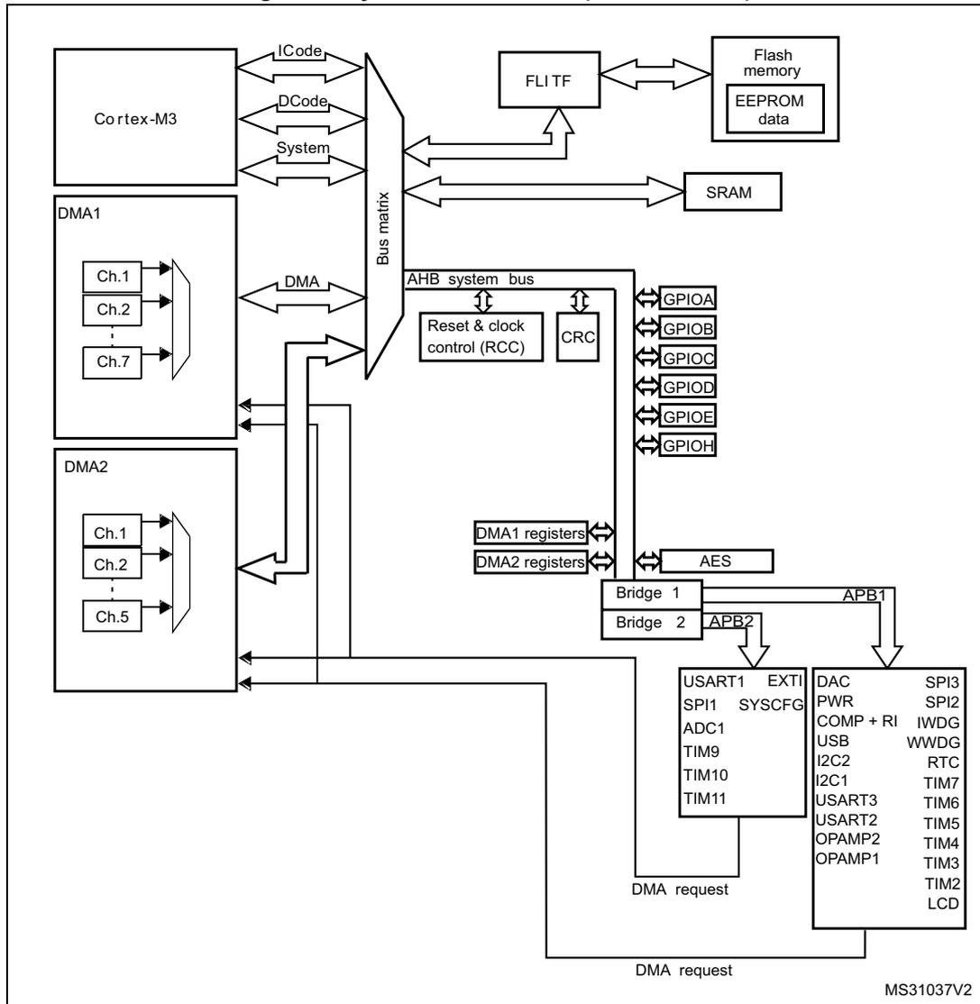
The diagram illustrates the system architecture for Cat.3 devices. At the core is the Cortex-M3 processor, which is connected to a Bus matrix via ICode, DCode, and System interfaces. The Bus matrix also connects to Flash memory (containing EEPROM data), SRAM, and the AHB system bus. The AHB system bus is connected to the Reset & clock control (RCC) and CRC blocks. DMA1 and DMA2 controllers are connected to the Bus matrix and the AHB system bus. DMA1 has channels Ch.1, Ch.2, and Ch.7. DMA2 has channels Ch.1, Ch.2, and Ch.5. The AHB system bus also connects to GPIOA, GPIOB, GPIOC, GPIOD, GPIOE, and GPIOH. DMA1 registers and DMA2 registers are connected to the AHB system bus. The AHB system bus connects to Bridge 1 and Bridge 2. Bridge 1 connects to APB1, which is connected to a block containing USART1, SPI1, ADC1, TIM9, TIM10, and TIM11. Bridge 2 connects to APB2, which is connected to a block containing DAC, PWR, COMP + RI, USB, I2C2, RTC, I2C1, USART3, USART2, OPAMP2, OPAMP1, SPI3, SPI2, IWDG, WWDG, RTC, TIM7, TIM6, TIM5, TIM4, TIM3, TIM2, and LCD. DMA requests are shown from the TIM9, TIM10, and TIM11 blocks to DMA1, and from the USART2 and OPAMP1 blocks to DMA2. The diagram is labeled MS31037V2.
Figure 3. System architecture (Cat.4 devices)
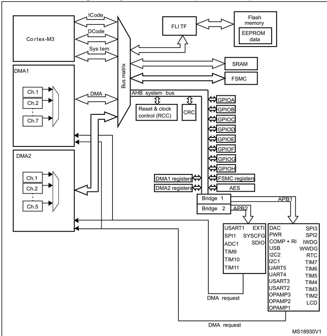
The diagram illustrates the system architecture for Cat.4 devices, centered around a Cortex-M3 processor connected to a Bus matrix. The Bus matrix is linked to the AHB system bus, which in turn connects to various components and bridges.
Cortex-M3 is connected to the Bus matrix via ICode, DCode, and System interfaces. FLITF (Flash Loader) is also connected to the Bus matrix and interfaces with Flash memory and EEPROM data .
The AHB system bus connects to SRAM , FSMC , Reset & clock control (RCC) , and CRC . DMA1 (channels Ch.1, Ch.2, ..., Ch.7) and DMA2 (channels Ch.1, Ch.2, ..., Ch.5) are connected to the Bus matrix and have associated registers (DMA1 registers, DMA2 registers).
GPIOs (GPIOA through GPIOH) are connected to the AHB system bus via a bridge. FSMC registers and AES are also connected to the AHB system bus.
Bridge 1 and Bridge 2 connect the AHB system bus to the APB1 and APB2 buses, respectively.
APB1 connects to a group of peripherals: USART1 , SPI1 , ADC1 , TIM9 , TIM10 , TIM11 , EXTI , SYSCFG , and SDIO . APB2 connects to a group of peripherals: DAC , PWR , COMP + RI , USB , I2C2 , I2C1 , UART5 , UART4 , USART3 , USART2 , OPAMP3 , OPAMP2 , OPAMP1 , SPI3 , SPI2 , IWDG , WWDG , RTC , TIM7 , TIM6 , TIM5 , TIM4 , TIM3 , TIM2 , and LCD .
DMA requests are shown from the peripherals on the APB buses to the DMA controllers.
Reference code: MS18930V1
Figure 4. System architecture (Cat.5 and Cat.6 devices)
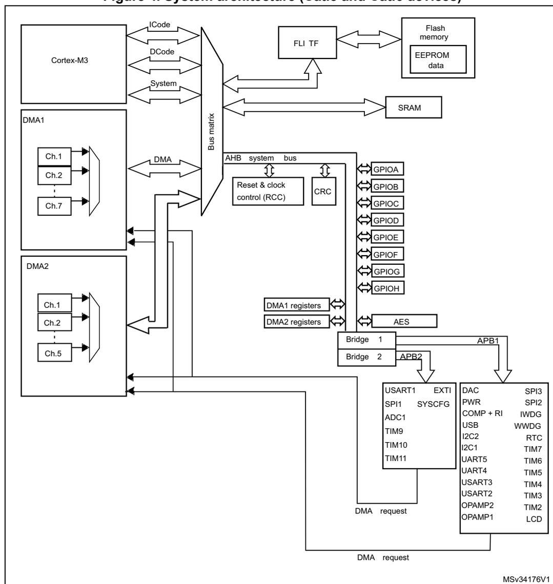
The diagram illustrates the system architecture for Cat.5 and Cat.6 devices. At the center is the Cortex-M3 core, which is connected to a Bus matrix via three buses: ICode (Instruction Code), DCode (Data Code), and System. The Bus matrix is connected to several components:
- FLI TF (Flash Interface) which is connected to Flash memory and EEPROM data.
- SRAM (Static Random Access Memory).
- AHB system bus, which includes Reset & clock control (RCC) and CRC (Cyclic Redundancy Check).
- GPIOs (GPIOA through GPIOH).
- DMA1 and DMA2 (Direct Memory Access) controllers with multiple channels (Ch.1 to Ch.7 for DMA1, Ch.1 to Ch.5 for DMA2).
- DMA1 registers and DMA2 registers.
- AES (Advanced Encryption Standard).
- Bridge 1 and Bridge 2, which connect to APB1 and APB2 buses respectively.
ICode bus
This bus connects the Instruction bus of the Cortex ® -M3 core to the BusMatrix. This bus is used by the core to fetch instructions. The target of this bus is a memory containing code (internal Flash memory or SRAM).
DCode bus
This bus connects the databus of the Cortex ® -M3 to the BusMatrix. This bus is used by the core for literal load and debug access. The target of this bus is a memory containing code or data (internal Flash memory or SRAM).
System bus
This bus connects the system bus of the Cortex ® -M3 core to a BusMatrix. This bus is used to access data located in a peripheral or in SRAM. Instructions may also be fetched on this bus (less efficient than ICode). The targets of this bus are the internal SRAM and the AHB/APB bridges.
DMA bus
This bus connects the AHB master interface of the DMA to the bus matrix which manages the access of the CPU DCode and DMA to the SRAM, Flash memory and peripherals.
Bus matrix
The bus matrix manages the access arbitration between the core system bus and the DMA master bus. The arbitration uses a round robin algorithm. The bus matrix is composed of five masters (ICode, DCode, System bus, DMA1 bus, DMA2 bus) and five slaves (Flash ICode interface, Flash DCode interface, SRAM, FSMC, and AHB2APB bridges).
AHB peripherals are connected on the system bus through the bus matrix to allow DMA access.
AHB/APB bridges (APB)
The two AHB/APB bridges provide full synchronous connections between the AHB and the 2 APB buses. The two APB buses operates at full speed (up to 32 MHz).
Refer to Table 5 on page 47 for the address mapping of the AHB and APB peripherals.
After each device reset, all peripheral clocks are disabled (except for the SRAM and Flash interface). Before using a peripheral, its clock should be enabled in the RCC_AHBENR, RCC_APB1ENR or RCC_APB2ENR register.
Note: When a 16- or 8-bit access is performed on an APB register, the access is transformed into a 32-bit access: the bridge duplicates the 16- or 8-bit data to feed the 32-bit vector.
2.2 Memory organization
SRAM, NVM, registers and I/O ports are organized within the same linear 4 Gbyte address space.
The bytes are coded in memory in little endian format. The lowest numbered byte in a word is considered the word's least significant byte and the highest numbered byte, the most significant.
For the detailed mapping of peripheral registers, refer to the related sections.
The addressable memory space is divided into 8 main blocks, each of 512 Mbytes.
All the memory areas that are not allocated to on-chip memories and peripherals are considered "Reserved". Refer to the memory map figure in the STM32L1xxxx datasheet.
2.3 Memory map
See the STM32L1xxxx datasheet for a comprehensive diagram of the memory map.
Table 5 gives the boundary addresses of the peripherals available in STM32L1xxxx devices.
Table 5. Register boundary addressesTable 5. Register boundary addresses (continued)
| Boundary address | Peripheral | Bus | Register map |
|---|---|---|---|
| 0x4000 7C00 - 0x4000 7C03 | COMP | APB1 | Section 14.9.2: COMP register map on page 343 |
| 0x4000 7C04 - 0x4000 7C5B | RI | Section 8.5.7: SYSCFG register map on page 222 | |
| 0x4000 7C5C - 0x4000 7FFF | OPAMP | Section 15.4.4: OPAMP register map on page 353 | |
| 0x4000 7400 - 0x4000 77FF | DAC | Section 13.5.15: DAC register map on page 331 | |
| 0x4000 7000 - 0x4000 73FF | PWR | Section 5.4.3: PWR register map on page 124 | |
| 0x4000 6000 - 0x4000 63FF | USB device FS SRAM 512 bytes | Section 24.5.4: USB register map on page 616 | |
| 0x4000 5C00 - 0x4000 5FFF | USB device FS | ||
| 0x4000 5800 - 0x4000 5BFF | I2C2 | Section 26.6.10: I2C register map on page 691 | |
| 0x4000 5400 - 0x4000 57FF | I2C1 | ||
| 0x4000 5000 - 0x4000 53FF | USART5 | Section 27.6.8: USART register map on page 743 | |
| 0x4000 4C00 - 0x4000 4FFF | USART4 | ||
| 0x4000 4800 - 0x4000 4BFF | USART3 | ||
| 0x4000 4400 - 0x4000 47FF | USART2 | ||
| 0x4000 3C00 - 0x4000 3FFF | SPI3 | Section 28.5.10: SPI register map on page 796 | |
| 0x4000 3800 - 0x4000 3BFF | SPI2 | ||
| 0x4000 3000 - 0x4000 33FF | IWDG | Section 21.4.5: IWDG register map on page 553 | |
| 0x4000 2C00 - 0x4000 2FFF | WWDG | Section 22.6.4: WWDG register map on page 560 | |
| 0x4000 2800 - 0x4000 2BFF | RTC | Section 20.6.21: RTC register map on page 546 | |
| 0x4000 2400 - 0x4000 27FF | LCD | Section 16.5.6: LCD register map on page 379 | |
| 0x4000 1400 - 0x4000 17FF | TIM7 | Section 19.4.9: TIM6 and TIM7 register map on page 506 | |
| 0x4000 1000 - 0x4000 13FF | TIM6 | ||
| 0x4000 0C00 - 0x4000 0FFF | TIM5 (32-bits) | Section 17.4.21: TIMx register map on page 440 | |
| 0x4000 0800 - 0x4000 0BFF | TIM4 | ||
| 0x4000 0400 - 0x4000 07FF | TIM3 | ||
| 0x4000 0000 - 0x4000 03FF | TIM2 |
2.4 Embedded SRAM
The STM32L1xxxx features up to 80 Kbytes of SRAM. It can be accessed as bytes, half-words (16 bits) or full words (32 bits). The SRAM start address is 0x2000 0000.
Read and write access at CPU speed with 0 wait states.
The CPU can access the SRAM through the system bus or through the I-Code/D-Code bus when boot in SRAM is selected or when physical remap is selected (see Section 8.5.1: SYSCFG memory remap register (SYSCFG_MEMRMP) register in the SYSCFG controller). To get the best SRAM execution performance, physical remap must be selected (boot or software selection).
2.5 NVM overview
The NVM is composed of three distinct physical areas:
- • The Flash program memory block. It contains the application program and optionally user data.
- • The Data EEPROM memory block. It contains user data.
- • The information block. It is composed of two parts:
- – Option bytes for hardware and memory protection user configuration.
- – System memory which contains the proprietary bootloader code. Refer to Section 3: Flash program memory and data EEPROM (FLASH) for more details.
NVM instructions and data access are performed through the AHB bus. The prefetch block is used for instruction fetches through the ICode bus. Arbitration is performed in the Flash memory interface, and priority is given to data access on the DCode bus. It also implements the logic necessary to carry out the Flash memory operations (Program/Erase) controlled through the Flash registers.
2.6 Bit banding
The Cortex ® -M3 memory map includes two bit-band regions. These regions map each word in an alias region of memory to a bit in a bit-band region of memory. Writing to a word in the alias region has the same effect as a read-modify-write operation on the targeted bit in the bit-band region.
In the STM32L1xxxx both the peripheral registers and the SRAM are mapped in a bit-band region. This allows single bit-band write and read operations to be performed. These operations are only available for Cortex ® -M3 accesses, not from other bus masters (e.g. DMA).
A mapping formula shows how to reference each word in the alias region to a corresponding bit in the bit-band region. The mapping formula is:
where:
bit_word_addr is the address of the word in the alias memory region that maps to the targeted bit
bit_band_base is the start address of the alias region
byte_offset is the number of the byte in the bit-band region, that contains the targeted bit
bit_number is the bit position (0-7) of the targeted bit
Example:
The following example shows how to map bit 2 of the byte located at SRAM address 0x2000 0300 in the alias region:
Writing to address 0x2200 6008 has the same effect as a read-modify-write operation on bit 2 of the byte at SRAM address 0x2000 0300.
Reading address 0x22006008 returns the value (0x01 or 0x00) of bit 2 of the byte at SRAM address 0x20000300 (0x01: bit set; 0x00: bit reset).
For more information on bit-banding, refer to the Cortex®-M3 Technical Reference Manual .
2.7 Boot configuration
Due to its fixed memory map, the code area starts from address 0x0000 0000 (accessed through the ICode/DCode buses) while the data area (SRAM) starts from address 0x2000 0000 (accessed through the system bus). The Cortex®-M3 CPU always fetches the reset vector from the ICode bus, which implies to have the boot space available only in the code area (typically, Flash memory). STM32L1xxxx microcontrollers implement a special mechanism to be able to boot from other memory than the Flash (like internal SRAM).
In the STM32L1xxxx, 3 different boot modes can be selected through the BOOT[1:0] pins as shown in Table 6 .
Table 6. Boot modes
| Option bit nBFB2 (1) | Boot mode selection pins | Boot mode | Aliasing | |
|---|---|---|---|---|
| BOOT1 | BOOT0 | |||
| 1 | x | 0 | Main Flash memory | Main Flash memory selected as the boot space |
| x | 0 | 1 | System memory | System memory selected as the boot space |
| x | 1 | 1 | Embedded SRAM | Embedded SRAM selected as the boot space |
| 0 | x | 0 | System memory | For Cat.4, Cat.5 and Cat.6 devices only. System memory is selected as the boot space, and the bootloader checks if jump to Bank2 or Bank1 is possible. Otherwise the bootloader execution continues. See nBFB2 bit description in Table 19: Description of the option bytes . |
1. nBFB2 option is present in Cat.4, Cat.5 and Cat.6 devices only. For Cat.1, Cat.2, Cat.3 devices behavior is like nBFB2=1.
The values on the BOOT pins are latched on the 4th rising edge of SYSCLK after a reset. It is up to the user to set the BOOT1 and BOOT0 pins after reset to select the required boot mode.
BOOT0 is a dedicated pin while BOOT1 is shared with a GPIO pin. Once BOOT1 has been sampled, the corresponding GPIO pin is free and can be used by the application.
The BOOT pins are also resampled when exiting the Standby mode. Consequently they must be kept in the required Boot mode configuration in Standby mode. After this startup delay has elapsed, the CPU fetches the top-of-stack value from address 0x0000 0000, then starts code execution from the boot memory starting from 0x0000 0004.
Note: When booting from SRAM, in the application initialization code, you have to relocate the vector table in SRAM using the NVIC exception table and offset register.
Physical remap
When the boot pins are configured as desired, the application software can modify the memory accessible in the code area (code can thus be executed through the ICode/DCode in place of the System bus). This modification is performed by programming the SYSCFG memory remap register (SYSCFG_MEMRMP) in the SYSCFG controller.
The following memory can then be remapped:
- • Main Flash memory
- • System memory
- • Embedded SRAM
Note: Depending on the memory protection programmed by option byte, some boot/remap configurations may not be available (refer to the readout protection section in Section 3: Flash program memory and data EEPROM (FLASH) for details).
Table 7. Memory mapping vs. boot mode/physical remap
| Addresses | Boot/Remap in main Flash memory | Boot/Remap in embedded SRAM | Boot/Remap in System memory |
|---|---|---|---|
| 0x2000 0000 - 0x2000 BFFF | SRAM | SRAM | SRAM |
| 0x1FF0 0000 - 0x1FF0 1FFF | System memory | System memory | System memory |
| 0x0802 0000 - 0x0FFF FFFF | Reserved | Reserved | Reserved |
| 0x0800 0000 - 0x0805 FFFF | Flash memory | Flash memory | Flash memory |
| 0x0002 0000 - 0x07FF FFFF | Reserved | Reserved | Reserved |
| 0x0000 0000 - 0x0005 FFFF | Flash (up to 512 Kbytes) Aliased | SRAM Aliased | System memory (8 Kbytes) Aliased |
Note: Even when aliased in the boot memory space, the related memory is still accessible at its original memory space.
Embedded boot loader
The embedded boot loader is used to reprogram the Flash memory through one of the following interfaces:
- • In Cat.1 and Cat.2 devices: USART1 or USART2.
- • In Cat.3, Cat.4, Cat.5 and Cat.6 devices: USART1, USART2 or USB
This program is located in the system memory and is programmed by ST during production.