25. Serial peripheral interface (SPI)
This section applies to the whole STM32F20x and STM32F21x family, unless otherwise specified.
25.1 SPI introduction
The SPI interface provides two main functions, supporting the SPI or the I 2 S audio protocol. By default, the SPI function is selected. It is possible to switch the interface from SPI to I 2 S by software.
The serial peripheral interface (SPI) allows half/ full-duplex, synchronous, serial communication with external devices. The interface can be configured as the master and in this case it provides the communication clock (SCK) to the external slave device. The interface is also capable of operating in multimaster configuration.
It may be used for a variety of purposes, including simplex synchronous transfers on two lines with a possible bidirectional data line or reliable communication using CRC checking.
The I 2 S is also a synchronous serial communication interface. It can address four different audio standards including the I 2 S Philips standard, the MSB- and LSB-justified standards, and the PCM standard. It can operate as a slave or a master device in full-duplex mode (using 4 pins) or in half-duplex mode (using 6 pins). Master clock can be provided by the interface to an external slave component when the I 2 S is configured as the communication master.
Warning: Since some SPI1 and SPI3/I2S3 pins may be mapped onto some pins used by the JTAG interface (SPI1_NSS onto JTDI, SPI3_NSS/I2S3_WS onto JTDI and SPI3_SCK/I2S3_CK onto JTDO), you may either:
- – map SPI/I2S onto other pins
- – disable the JTAG and use the SWD interface prior to configuring the pins listed as SPI I/Os (when debugging the application) or
- – disable both JTAG/SWD interfaces (for standalone applications).
For more information on the configuration of the JTAG/SWD interface pins, refer to Section 6.3.2: I/O pin multiplexer and mapping .
25.2 SPI and I 2 S main features
25.2.1 SPI features
- • Full-duplex synchronous transfers on three lines
- • Simplex synchronous transfers on two lines with or without a bidirectional data line
- • 8- or 16-bit transfer frame format selection
- • Master or slave operation
- • Multimaster mode capability
- • 8 master mode baud rate prescalers ( \( f_{PCLK}/2 \) max.)
- • Slave mode frequency ( \( f_{PCLK}/2 \) max)
- • Faster communication for both master and slave
- • NSS management by hardware or software for both master and slave: dynamic change of master/slave operations
- • Programmable clock polarity and phase
- • Programmable data order with MSB-first or LSB-first shifting
- • Dedicated transmission and reception flags with interrupt capability
- • SPI bus busy status flag
- • SPI TI mode
- • Hardware CRC feature for reliable communication:
- – CRC value can be transmitted as last byte in Tx mode
- – Automatic CRC error checking for last received byte
- • Master mode fault, overrun and CRC error flags with interrupt capability
- • 1-byte transmission and reception buffer with DMA capability: Tx and Rx requests
25.2.2 I 2 S features
- • Half-duplex communication (only transmitter or receiver)
- • Master or slave operations
- • 8-bit programmable linear prescaler to reach accurate audio sample frequencies (from 8 kHz to 192 kHz)
- • Data format may be 16-bit, 24-bit or 32-bit
- • Packet frame is fixed to 16-bit (16-bit data frame) or 32-bit (16-bit, 24-bit, 32-bit data frame) by audio channel
- • Programmable clock polarity (steady state)
- • Underrun flag in slave transmission mode and Overrun flag in reception mode (master and slave)
- • 16-bit register for transmission and reception with one data register for both channel sides
- • Supported I
2
S protocols:
- – I 2 S Phillips standard
- – MSB-justified standard (left-justified)
- – LSB-justified standard (right-justified)
- – PCM standard (with short and long frame synchronization on 16-bit channel frame or 16-bit data frame extended to 32-bit channel frame)
- • Data direction is always MSB first
- • DMA capability for transmission and reception (16-bit wide)
- • Master clock may be output to drive an external audio component. Ratio is fixed at \( 256 \times F_S \) (where \( F_S \) is the audio sampling frequency)
25.3 SPI functional description
25.3.1 General description
The block diagram of the SPI is shown in Figure 248 .
![Figure 248. SPI block diagram. This diagram illustrates the internal architecture of an SPI peripheral. On the left, four pins are shown: MOSI, MISO, SCK, and NSS. The MOSI and MISO pins are connected to a bidirectional data path. The SCK pin is connected to a Baud rate generator and Master control logic. The NSS pin is connected to the Master control logic. The internal components include a 'Read' path from the Address and data bus to an 'Rx buffer', a 'Shift register' (configured for LSB first), and a 'Tx buffer' which receives data from the Address and data bus via a 'Write' path. The Shift register is connected to the MOSI/MISO pins. The Rx buffer and Tx buffer are connected to the Address and data bus. The Communication control block receives inputs from the Baud rate generator (BR[2:0]), Master control logic, and SPI registers (SPI_CR1, SPI_CR2, SPI_SR). The SPI_CR1 register contains bits for LSB FIRST, SPE, BR2, BR1, BR0, MSTR, CPOL, CPHA, BIDI MODE, BIDI OE, CRCEN, CRC Next, DFF, RX ONLY, SSM, and SSI. The SPI_CR2 register contains bits for TXE IE, RXNE IE, ERR IE, 0, 0, SSOE, TXDM AEN, and RXDM AEN. The SPI_SR register contains bits for BSY, OVR, MOD F, CRC ERR, 0, 0, TXE, and RXNE. The Communication control block also has a 0/1 input and is connected to the Address and data bus.](/RM0033-STM32F205-207-215-217/12f4c2b85b663fd76dceb3683a570c1d_img.jpg)
Figure 248. SPI block diagram
Usually, the SPI is connected to external devices through four pins:
- • MISO: Master In / Slave Out data. This pin can be used to transmit data in slave mode and receive data in master mode.
- • MOSI: Master Out / Slave In data. This pin can be used to transmit data in master mode and receive data in slave mode.
- • SCK: Serial Clock output for SPI masters and input for SPI slaves.
- • NSS: Slave select. This is an optional pin to select a slave device. This pin acts as a 'chip select' to let the SPI master communicate with slaves individually and to avoid contention on the data lines. Slave NSS inputs can be driven by standard IO ports on the master device. The NSS pin may also be used as an output if enabled (SSOE bit) and driven low if the SPI is in master configuration. In this manner, all NSS pins from devices connected to the Master NSS pin see a low level and become slaves when they are configured in NSS hardware mode. When configured in master mode with NSS configured as an input (MSTR=1 and SSOE=0) and if NSS is pulled low, the SPI enters the master mode fault state: the MSTR bit is automatically cleared and the device is configured in slave mode (refer to Section 25.3.10 ).
A basic example of interconnections between a single master and a single slave is illustrated in Figure 249 .
Figure 249. Single master/single slave application
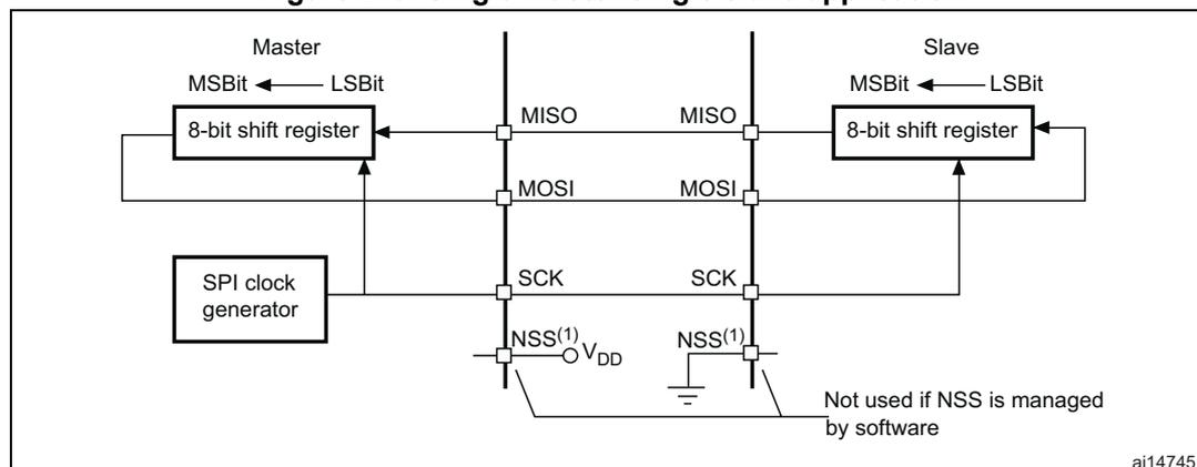
- 1. Here, the NSS pin is configured as an input.
The MOSI pins are connected together and the MISO pins are connected together. In this way data is transferred serially between master and slave (most significant bit first).
The communication is always initiated by the master. When the master device transmits data to a slave device via the MOSI pin, the slave device responds via the MISO pin. This implies full-duplex communication with both data out and data in synchronized with the same clock signal (which is provided by the master device via the SCK pin).
Slave select (NSS) pin management
Hardware or software slave select management can be set using the SSM bit in the SPI_CR1 register.
- • Software NSS management (SSM = 1)
The slave select information is driven internally by the value of the SSI bit in the SPI_CR1 register. The external NSS pin remains free for other application uses.
- • Hardware NSS management (SSM = 0)
Two configurations are possible depending on the NSS output configuration (SSOE bit in register SPI_CR2).
- – NSS output enabled (SSM = 0, SSOE = 1)
This configuration is used only when the device operates in master mode. The NSS signal is driven low when the master starts the communication and is kept low until the SPI is disabled.
- – NSS output disabled (SSM = 0, SSOE = 0)
This configuration allows multimaster capability for devices operating in master mode. For devices set as slave, the NSS pin acts as a classical NSS input: the slave is selected when NSS is low and deselected when NSS high.
Clock phase and clock polarity
Four possible timing relationships may be chosen by software, using the CPOL and CPHA bits in the SPI_CR1 register. The CPOL (clock polarity) bit controls the steady state value of the clock when no data is being transferred. This bit affects both master and slave modes. If CPOL is reset, the SCK pin has a low-level idle state. If CPOL is set, the SCK pin has a high-level idle state.
If the CPHA (clock phase) bit is set, the second edge on the SCK pin (falling edge if the CPOL bit is reset, rising edge if the CPOL bit is set) is the MSBit capture strobe. Data are
latched on the occurrence of the second clock transition. If the CPHA bit is reset, the first edge on the SCK pin (falling edge if CPOL bit is set, rising edge if CPOL bit is reset) is the MSBit capture strobe. Data are latched on the occurrence of the first clock transition.
The combination of the CPOL (clock polarity) and CPHA (clock phase) bits selects the data capture clock edge.
Figure 250 , shows an SPI transfer with the four combinations of the CPHA and CPOL bits. The diagram may be interpreted as a master or slave timing diagram where the SCK pin, the MISO pin, the MOSI pin are directly connected between the master and the slave device.
Note:
Prior to changing the CPOL/CPHA bits the SPI must be disabled by resetting the SPE bit.
Master and slave must be programmed with the same timing mode.
The idle state of SCK must correspond to the polarity selected in the SPI_CR1 register (by pulling up SCK if CPOL=1 or pulling down SCK if CPOL=0).
The Data Frame Format (8- or 16-bit) is selected through the DFF bit in SPI_CR1 register, and determines the data length during transmission/reception.
Figure 250. Data clock timing diagram
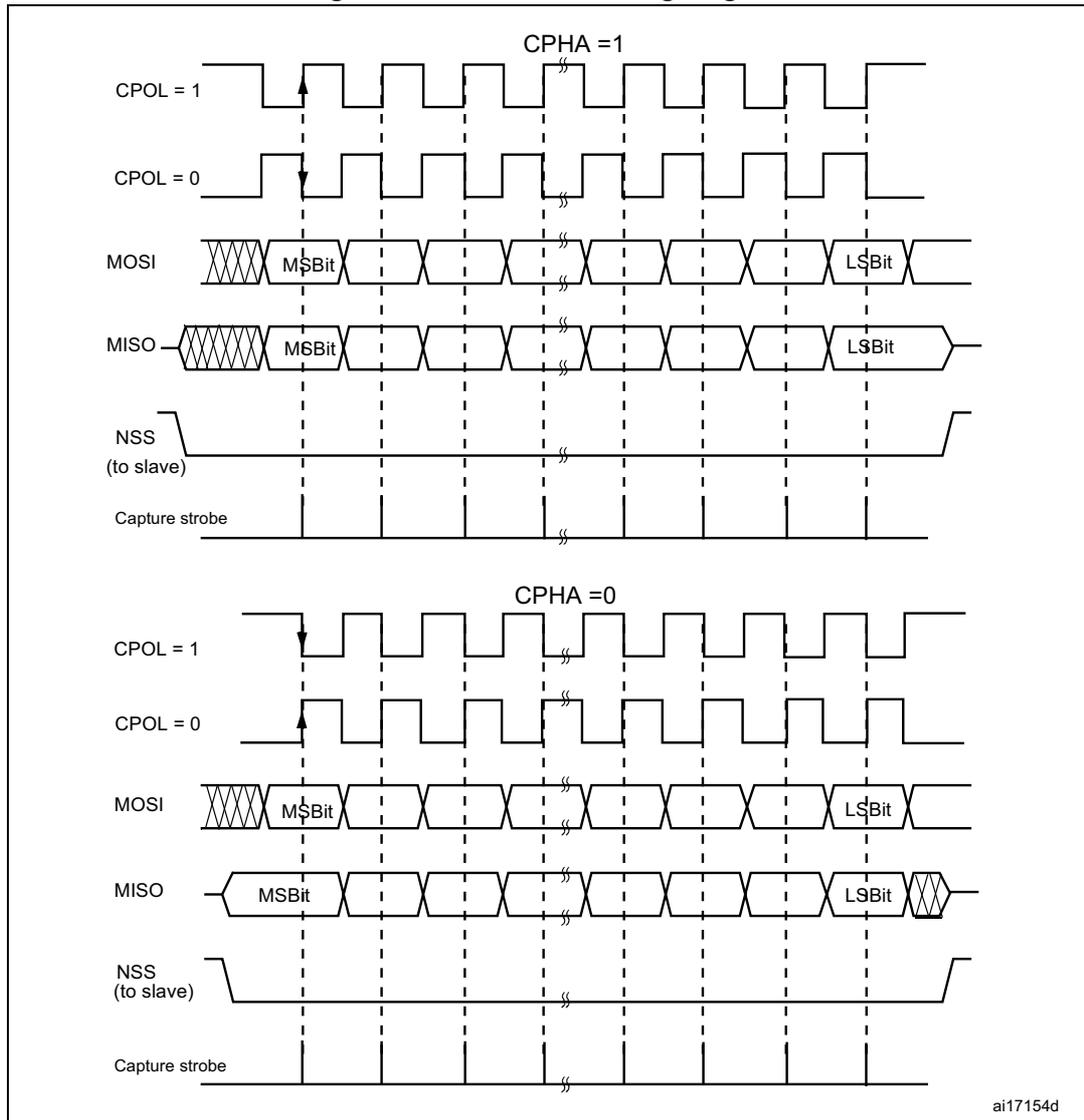
The figure contains two timing diagrams for SPI data transfer. The top diagram is for CPHA = 1, and the bottom diagram is for CPHA = 0. Both diagrams show the relationship between the clock signal (CPOL = 1 and CPOL = 0), the Master Out Slave In (MOSI) signal, the Master In Slave Out (MISO) signal, the Slave Select (NSS) signal, and the capture strobe. In the CPHA = 1 diagram, data is captured on the second clock edge of each frame. In the CPHA = 0 diagram, data is captured on the first clock edge of each frame. The MOSI and MISO signals are shown with the Most Significant Bit (MSB) and Least Significant Bit (LSB) indicated. The NSS signal is shown as a low-active signal. The capture strobe is shown as a pulse that occurs on the second clock edge of each frame in the CPHA = 1 diagram and on the first clock edge in the CPHA = 0 diagram. The diagrams are labeled 'ai17154d' in the bottom right corner.
1. These timings are shown with the LSBFIRST bit reset in the SPI_CR1 register.
Data frame format
Data can be shifted out either MSB-first or LSB-first depending on the value of the LSBFIRST bit in the SPI_CR1 register.
Each data frame is 8 or 16 bits long depending on the size of the data programmed using the DFF bit in the SPI_CR1 register. The selected data frame format is applicable for transmission and/or reception.
25.3.2 Configuring the SPI in slave mode
In the slave configuration, the serial clock is received on the SCK pin from the master device. The value set in the BR[2:0] bits in the SPI_CR1 register, does not affect the data transfer rate.
Note: It is recommended to enable the SPI slave before the master sends the clock. If not, undesired data transmission might occur. The data register of the slave needs to be ready before the first edge of the communication clock or before the end of the ongoing communication. It is mandatory to have the polarity of the communication clock set to the steady state value before the slave and the master are enabled.
Follow the procedure below to configure the SPI in slave mode:
Procedure
- 1. Set the DFF bit to define 8- or 16-bit data frame format
- 2. Select the CPOL and CPHA bits to define one of the four relationships between the data transfer and the serial clock (see Figure 250 ). For correct data transfer, the CPOL and CPHA bits must be configured in the same way in the slave device and the master device. This step is not required when the TI mode is selected through the FRF bit in the SPI_CR2 register.
- 3. The frame format (MSB-first or LSB-first depending on the value of the LSBFIRST bit in the SPI_CR1 register) must be the same as the master device. This step is not required when TI mode is selected.
- 4. In Hardware mode (refer to Slave select (NSS) pin management ), the NSS pin must be connected to a low level signal during the complete byte transmit sequence. In NSS software mode, set the SSM bit and clear the SSI bit in the SPI_CR1 register. This step is not required when TI mode is selected.
- 5. Set the FRF bit in the SPI_CR2 register to select the TI mode protocol for serial communications.
- 6. Clear the MSTR bit and set the SPE bit (both in the SPI_CR1 register) to assign the pins to alternate functions.
In this configuration the MOSI pin is a data input and the MISO pin is a data output.
Transmit sequence
The data byte is parallel-loaded into the Tx buffer during a write cycle.
The transmit sequence begins when the slave device receives the clock signal and the most significant bit of the data on its MOSI pin. The remaining bits (the 7 bits in 8-bit data frame format, and the 15 bits in 16-bit data frame format) are loaded into the shift-register. The TXE flag in the SPI_SR register is set on the transfer of data from the Tx Buffer to the shift register and an interrupt is generated if the TXEIE bit in the SPI_CR2 register is set.
Receive sequence
For the receiver, when data transfer is complete:
- • The Data in shift register is transferred to Rx Buffer and the RXNE flag (SPI_SR register) is set
- • An Interrupt is generated if the RXNEIE bit is set in the SPI_CR2 register.
After the last sampling clock edge the RXNE bit is set, a copy of the data byte received in the shift register is moved to the Rx buffer. When the SPI_DR register is read, the SPI peripheral returns this buffered value.
Clearing of the RXNE bit is performed by reading the SPI_DR register.
SPI TI protocol in slave mode
In slave mode, the SPI interface is compatible with the TI protocol. The FRF bit of the SPI_CR2 register can be used to configure the slave SPI serial communications to be compliant with this protocol.
The clock polarity and phase are forced to conform to the TI protocol requirements whatever the values set in the SPI_CR1 register. NSS management is also specific to the TI protocol which makes the configuration of NSS management through the SPI_CR1 and SPI_CR2 registers (such as SSM, SSI, SSOE) transparent for the user.
In Slave mode (Figure 251 and Figure 252), the SPI baud rate prescaler is used to control the moment when the MISO pin state changes to HI-Z. Any baud rate can be used thus allowing to determine this moment with optimal flexibility. However, the baud rate is generally set to the external master clock baud rate. The time for the MISO signal to become HI-Z ( \( t_{\text{release}} \) ) depends on internal resynchronizations and on the baud rate value set in through BR[2:0] of SPI_CR1 register. It is given by the formula:
Note: This feature is not available for Motorola SPI communications (FRF bit set to 0).
To detect TI frame errors in Slave transmitter only mode by using the Error interrupt (ERRIE = 1), the SPI must be configured in 1-line bidirectional mode by setting BIDIMODE and BIDIOE to 1 in the SPI_CR1 register. When BIDIMODE is set to 0, OVR is set to 1 because the data register is never read and error interrupt are always generated, while when BIDIMODE is set to 1, data are not received and OVR is never set.
Figure 251. TI mode - Slave mode, single transfer
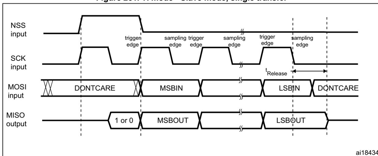
The diagram illustrates the timing for a single transfer in SPI TI mode - Slave mode. The signals shown are:
- NSS input: Active-low signal. It goes low to start the transfer and high to end it. The falling edge is the 'trigger edge'.
- SCK input: Square wave clock signal. The 'trigger edge' is the rising edge, and the 'sampling edge' is the falling edge.
- MOSI input: Master Out Slave In signal. It is labeled 'DONT CARE' at the beginning and end, and 'MSBIN' and 'LSBIN' in the middle.
- MISO output: Master In Slave Out signal. It is labeled '1 or 0' at the beginning, 'MSBOUT' and 'LSBOUT' in the middle, and 'DONT CARE' at the end. The signal goes high-Z after the last sampling edge.
The time interval \( t_{\text{Release}} \) is shown between the last sampling edge and the MISO output going high-Z.
ai18434
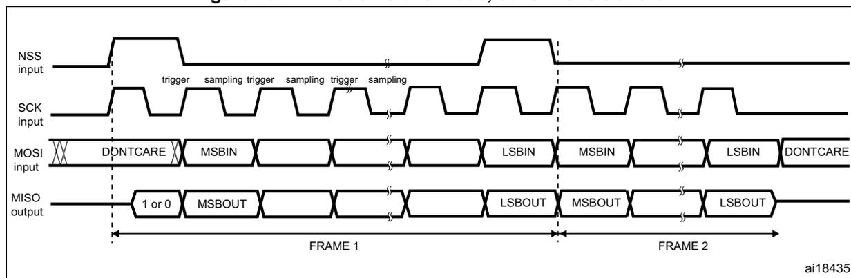
Figure 252. TI mode - Slave mode, continuous transfer
25.3.3 Configuring the SPI in master mode
In the master configuration, the serial clock is generated on the SCK pin.
Procedure
- 1. Select the BR[2:0] bits to define the serial clock baud rate (see SPI_CR1 register).
- 2. Select the CPOL and CPHA bits to define one of the four relationships between the data transfer and the serial clock (see Figure 250). This step is not required when the TI mode is selected.
- 3. Set the DFF bit to define 8- or 16-bit data frame format
- 4. Configure the LSBFIRST bit in the SPI_CR1 register to define the frame format. This step is not required when the TI mode is selected.
- 5. If the NSS pin is required in input mode, in hardware mode, connect the NSS pin to a high-level signal during the complete byte transmit sequence. In NSS software mode, set the SSM and SSI bits in the SPI_CR1 register. If the NSS pin is required in output mode, the SSOE bit only should be set. This step is not required when the TI mode is selected.
- 6. Set the FRF bit in SPI_CR2 to select the TI protocol for serial communications.
- 7. The MSTR and SPE bits must be set (they remain set only if the NSS pin is connected to a high-level signal).
In this configuration the MOSI pin is a data output and the MISO pin is a data input.
Transmit sequence
The transmit sequence begins when a byte is written in the Tx Buffer.
The data byte is parallel-loaded into the shift register (from the internal bus) during the first bit transmission and then shifted out serially to the MOSI pin MSB first or LSB first depending on the LSBFIRST bit in the SPI_CR1 register. The TXE flag is set on the transfer of data from the Tx Buffer to the shift register and an interrupt is generated if the TXEIE bit in the SPI_CR2 register is set.
Receive sequence
For the receiver, when data transfer is complete:
- • The data in the shift register is transferred to the RX Buffer and the RXNE flag is set
- • An interrupt is generated if the RXNEIE bit is set in the SPI_CR2 register
At the last sampling clock edge the RXNE bit is set, a copy of the data byte received in the shift register is moved to the Rx buffer. When the SPI_DR register is read, the SPI peripheral returns this buffered value.
Clearing the RXNE bit is performed by reading the SPI_DR register.
A continuous transmit stream can be maintained if the next data to be transmitted is put in the Tx buffer once the transmission is started. Note that TXE flag should be ‘1 before any attempt to write the Tx buffer is made.
Note: When a master is communicating with SPI slaves which need to be de-selected between transmissions, the NSS pin must be configured as GPIO or another GPIO must be used and toggled by software.
SPI TI protocol in master mode
In master mode, the SPI interface is compatible with the TI protocol. The FRF bit of the SPI_CR2 register can be used to configure the master SPI serial communications to be compliant with this protocol.
The clock polarity and phase are forced to conform to the TI protocol requirements whatever the values set in the SPI_CR1 register. NSS management is also specific to the TI protocol which makes the configuration of NSS management through the SPI_CR1 and SPI_CR2 registers (SSM, SSI, SSOE) transparent for the user.
Figure 253 and Figure 254 show the SPI master communication waveforms when the TI mode is selected in master mode.
Figure 253. TI mode - master mode, single transfer
The timing diagram illustrates a single data transfer in SPI TI master mode.
- NSS output: Pulses high to indicate the start of a frame. It goes low at the first 'triggen edge' (falling edge of SCK) and stays low until after the last 'sampling edge'.
- SCK output: The serial clock. The first falling edge is labeled 'triggen edge'. Subsequent rising edges are 'sampling edges'. The final falling edge is also a 'trigger edge'.
- MOSI input: Data is sampled on the rising edges of SCK. It transitions from 'DONTCARE' to 'MSBIN' at the first trigger edge, and ends with 'LSBIN' followed by 'DONTCARE'.
- MISO output: Data is driven on the falling edges of SCK. It transitions from '1 or 0' to 'MSBOUT' at the first trigger edge, and ends with 'LSBOUT'.
ai18436
Figure 254. TI mode - master mode, continuous transfer
25.3.4 Configuring the SPI for half-duplex communication
The SPI is capable of operating in half-duplex mode in 2 configurations.
- • 1 clock and 1 bidirectional data wire
- • 1 clock and 1 data wire (receive-only or transmit-only)
1 clock and 1 bidirectional data wire (BIDIMODE = 1)
This mode is enabled by setting the BIDIMODE bit in the SPI_CR1 register. In this mode SCK is used for the clock and MOSI in master or MISO in slave mode is used for data communication. The transfer direction (Input/Output) is selected by the BIDIOE bit in the SPI_CR1 register. When this bit is 1, the data line is output otherwise it is input.
1 clock and 1 unidirectional data wire (BIDIMODE = 0)
In this mode, the application can use the SPI either in transmit-only mode or in receive-only mode.
- • Transmit-only mode is similar to full-duplex mode (BIDIMODE=0, RXONLY=0): the data are transmitted on the transmit pin (MOSI in master mode or MISO in slave mode) and the receive pin (MISO in master mode or MOSI in slave mode) can be used as a general-purpose IO. In this case, the application just needs to ignore the Rx buffer (if the data register is read, it does not contain the received value).
- • In receive-only mode, the application can disable the SPI output function by setting the RXONLY bit in the SPI_CR1 register. In this case, it frees the transmit IO pin (MOSI in master mode or MISO in slave mode), so it can be used for other purposes.
To start the communication in receive-only mode, configure and enable the SPI:
- • In master mode, the communication starts immediately and stops when the SPE bit is cleared and the current reception stops. There is no need to read the BSY flag in this mode. It is always set when an SPI communication is ongoing.
- • In slave mode, the SPI continues to receive as long as the NSS is pulled down (or the SSI bit is cleared in NSS software mode) and the SCK is running.
25.3.5 Data transmission and reception procedures
Rx and Tx buffers
In reception, data are received and then stored into an internal Rx buffer while In transmission, data are first stored into an internal Tx buffer before being transmitted.
A read access of the SPI_DR register returns the Rx buffered value whereas a write access to the SPI_DR stores the written data into the Tx buffer.
Start sequence in master mode
- • In full-duplex (BIDIMODE=0 and RXONLY=0)
- – The sequence begins when data are written into the SPI_DR register (Tx buffer).
- – The data are then parallel loaded from the Tx buffer into the 8-bit shift register during the first bit transmission and then shifted out serially to the MOSI pin.
- – At the same time, the received data on the MISO pin is shifted in serially to the 8-bit shift register and then parallel loaded into the SPI_DR register (Rx buffer).
- • In unidirectional receive-only mode (BIDIMODE=0 and RXONLY=1)
- – The sequence begins as soon as SPE=1
- – Only the receiver is activated and the received data on the MISO pin are shifted in serially to the 8-bit shift register and then parallel loaded into the SPI_DR register (Rx buffer).
- • In bidirectional mode, when transmitting (BIDIMODE=1 and BIDIOE=1)
- – The sequence begins when data are written into the SPI_DR register (Tx buffer).
- – The data are then parallel loaded from the Tx buffer into the 8-bit shift register during the first bit transmission and then shifted out serially to the MOSI pin.
- – No data are received.
- • In bidirectional mode, when receiving (BIDIMODE=1 and BIDIOE=0)
- – The sequence begins as soon as SPE=1 and BIDIOE=0.
- – The received data on the MOSI pin are shifted in serially to the 8-bit shift register and then parallel loaded into the SPI_DR register (Rx buffer).
- – The transmitter is not activated and no data are shifted out serially to the MOSI pin.
Start sequence in slave mode
- • In full-duplex mode (BIDIMODE=0 and RXONLY=0)
- – The sequence begins when the slave device receives the clock signal and the first bit of the data on its MOSI pin. The 7 remaining bits are loaded into the shift register.
- – At the same time, the data are parallel loaded from the Tx buffer into the 8-bit shift register during the first bit transmission, and then shifted out serially to the MISO pin. The software must have written the data to be sent before the SPI master device initiates the transfer.
- • In unidirectional receive-only mode (BIDIMODE=0 and RXONLY=1)
- – The sequence begins when the slave device receives the clock signal and the first bit of the data on its MOSI pin. The 7 remaining bits are loaded into the shift register.
- – The transmitter is not activated and no data are shifted out serially to the MISO pin.
- • In bidirectional mode, when transmitting (BIDIMODE=1 and BIDIOE=1)
- – The sequence begins when the slave device receives the clock signal and the first bit in the Tx buffer is transmitted on the MISO pin.
- – The data are then parallel loaded from the Tx buffer into the 8-bit shift register during the first bit transmission and then shifted out serially to the MISO pin. The software must have written the data to be sent before the SPI master device initiates the transfer.
- – No data are received.
- • In bidirectional mode, when receiving (BIDIMODE=1 and BIDIOE=0)
- – The sequence begins when the slave device receives the clock signal and the first bit of the data on its MISO pin.
- – The received data on the MISO pin are shifted in serially to the 8-bit shift register and then parallel loaded into the SPI_DR register (Rx buffer).
- – The transmitter is not activated and no data are shifted out serially to the MISO pin.
Handling data transmission and reception
The TXE flag (Tx buffer empty) is set when the data are transferred from the Tx buffer to the shift register. It indicates that the internal Tx buffer is ready to be loaded with the next data. An interrupt can be generated if the TXEIE bit in the SPI_CR2 register is set. Clearing the TXE bit is performed by writing to the SPI_DR register.
Note: The software must ensure that the TXE flag is set to 1 before attempting to write to the Tx buffer. Otherwise, it overwrites the data previously written to the Tx buffer.
The RXNE flag (Rx buffer not empty) is set on the last sampling clock edge, when the data are transferred from the shift register to the Rx buffer. It indicates that data are ready to be read from the SPI_DR register. An interrupt can be generated if the RXNEIE bit in the SPI_CR2 register is set. Clearing the RXNE bit is performed by reading the SPI_DR register.
For some configurations, the BSY flag can be used during the last data transfer to wait until the completion of the transfer.
Full-duplex transmit and receive procedure in master or slave mode (BIDIMODE=0 and RXONLY=0)
The software has to follow this procedure to transmit and receive data (see Figure 255 and Figure 256 ):
- 1. Enable the SPI by setting the SPE bit to 1.
- 2. Write the first data item to be transmitted into the SPI_DR register (this clears the TXE flag).
- 3. Wait until TXE=1 and write the second data item to be transmitted. Then wait until RXNE=1 and read the SPI_DR to get the first received data item (this clears the RXNE bit). Repeat this operation for each data item to be transmitted/received until the n–1 received data.
- 4. Wait until RXNE=1 and read the last received data.
- 5. Wait until TXE=1 and then wait until BSY=0 before disabling the SPI.
This procedure can also be implemented using dedicated interrupt subroutines launched at each rising edges of the RXNE or TXE flag.
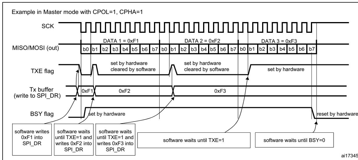
Figure 255. TXE/RXNE/BSY behavior in Master / full-duplex mode (BIDIMODE=0 and RXONLY=0) in case of continuous transfers
Example in Master mode with CPOL=1, CPHA=1
The diagram illustrates the timing and control signals for SPI Master mode full-duplex continuous transfers. The signals shown are:
- SCK: Serial clock signal, shown as a continuous square wave.
- MISO/MOSI (out): Master In Slave Out / Master Out Slave In (out) signal. It shows the transmission of three data bytes: DATA1 = 0xF1, DATA2 = 0xF2, and DATA3 = 0xF3. Each byte is transmitted in 8 bits (b0 to b7).
- TXE flag: Transmit buffer empty flag. It is set by hardware when the buffer is empty and cleared by software when a new value is written.
- Tx buffer (write SPI_DR): Transmit buffer. It contains the data to be transmitted: 0xF1, 0xF2, and 0xF3.
- BSY flag: Busy flag. It is set by hardware when the transfer starts and reset by hardware when the transfer is complete.
- MISO/MOSI (in): Master In Slave Out / Master Out Slave In (in) signal. It shows the reception of three data bytes: DATA 1 = 0xA1, DATA 2 = 0xA2, and DATA 3 = 0xA3. Each byte is received in 8 bits (b0 to b7).
- RXNE flag: Receive buffer not empty flag. It is set by hardware when the buffer is not empty and cleared by software when the data is read.
- Rx buffer (read SPI_DR): Receive buffer. It contains the data received: 0xA1, 0xA2, and 0xA3.
The sequence of software operations shown at the bottom of the diagram is:
- software writes 0xF1 into SPI_DR
- software waits until TXE=1 and writes 0xF2 into SPI_DR
- software waits until RXNE=1 and reads 0xA1 from SPI_DR
- software waits until TXE=1 and writes 0xF3 into SPI_DR
- software waits until RXNE=1 and reads 0xA2 from SPI_DR
- software waits until RXNE=1 and reads 0xA3 from SPI_DR
ai17343
Figure 256. TXE/RXNE/BSY behavior in Slave / full-duplex mode (BIDIMODE=0, RXONLY=0) in case of continuous transfers
Example in Slave mode with CPOL=1, CPHA=1
MSV76802V1
Transmit-only procedure (BIDIMODE=0 RXONLY=0)
In this mode, the procedure can be reduced as described below and the BSY bit can be used to wait until the completion of the transmission (see Figure 257 and Figure 258 ).
- 1. Enable the SPI by setting the SPE bit to 1.
- 2. Write the first data item to send into the SPI_DR register (this clears the TXE bit).
- 3. Wait until TXE=1 and write the next data item to be transmitted. Repeat this step for each data item to be transmitted.
- 4. After writing the last data item into the SPI_DR register, wait until TXE=1, then wait until BSY=0, this indicates that the transmission of the last data is complete.
This procedure can be also implemented using dedicated interrupt subroutines launched at each rising edge of the TXE flag.
Note: During discontinuous communications, there is a 2 APB clock period delay between the write operation to SPI_DR and the BSY bit setting. As a consequence, in transmit-only mode, it is mandatory to wait first until TXE is set and then until BSY is cleared after writing the last data.
After transmitting two data items in transmit-only mode, the OVR flag is set in the SPI_SR register since the received data are never read.
Figure 257. TXE/BSY behavior in Master transmit-only mode (BIDIMODE=0 and RXONLY=0) in case of continuous transfers
Example in Master mode with CPOL=1, CPHA=1
The diagram illustrates the timing and control signals for a Master transmit-only SPI transfer. The SCK signal is a continuous square wave. The MISO/MOSI (out) line transmits DATA 1 = 0xF1, DATA 2 = 0xF2, and DATA 3 = 0xF3, each represented by 8 bits (b0 to b7). The TXE flag is set by hardware when the Tx buffer is empty and cleared by software when the buffer is loaded. The Tx buffer (write to SPI_DR) contains the data to be transmitted. The BSY flag is set by hardware when the SPI is active and reset by hardware when the transfer is complete. The software sequence is: write 0xF1 into SPI_DR, wait until TXE=1 and write 0xF2 into SPI_DR, wait until TXE=1 and write 0xF3 into SPI_DR, wait until TXE=1, and finally wait until BSY=0.
ai17345
Figure 258. TXE/BSY in Slave transmit-only mode (BIDIMODE=0 and RXONLY=0) in case of continuous transfers
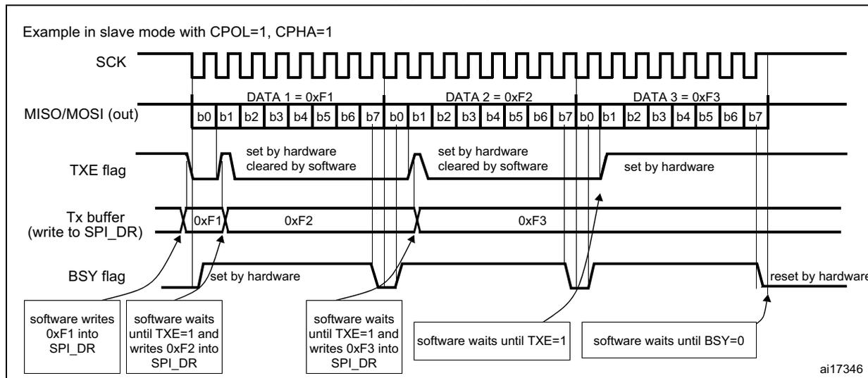
Example in slave mode with CPOL=1, CPHA=1
The diagram illustrates the timing and control signals for a Slave transmit-only SPI transfer. The SCK signal is a continuous square wave. The MISO/MOSI (out) line transmits DATA 1 = 0xF1, DATA 2 = 0xF2, and DATA 3 = 0xF3, each represented by 8 bits (b0 to b7). The TXE flag is set by hardware when the Tx buffer is empty and cleared by software when the buffer is loaded. The Tx buffer (write to SPI_DR) contains the data to be transmitted. The BSY flag is set by hardware when the SPI is active and reset by hardware when the transfer is complete. The software sequence is: write 0xF1 into SPI_DR, wait until TXE=1 and write 0xF2 into SPI_DR, wait until TXE=1 and write 0xF3 into SPI_DR, wait until TXE=1, and finally wait until BSY=0.
ai17346
Bidirectional transmit procedure (BIDIMODE=1 and BIDIOE=1)
In this mode, the procedure is similar to the procedure in Transmit-only mode except that the BIDIMODE and BIDIOE bits both have to be set in the SPI_CR2 register before enabling the SPI.
Unidirectional receive-only procedure (BIDIMODE=0 and RXONLY=1)
In this mode, the procedure can be reduced as described below (see Figure 259 ):
- 1. Set the RXONLY bit in the SPI_CR1 register.
- 2. Enable the SPI by setting the SPE bit to 1:
- a) In master mode, this immediately activates the generation of the SCK clock, and data are serially received until the SPI is disabled (SPE=0).
- b) In slave mode, data are received when the SPI master device drives NSS low and generates the SCK clock.
- 3. Wait until RXNE=1 and read the SPI_DR register to get the received data (this clears the RXNE bit). Repeat this operation for each data item to be received.
This procedure can also be implemented using dedicated interrupt subroutines launched at each rising edge of the RXNE flag.
Note: If it is required to disable the SPI after the last transfer, follow the recommendation described in Section 25.3.8 .
Figure 259. RXNE behavior in receive-only mode (BIDIRMODE=0 and RXONLY=1) in case of continuous transfers
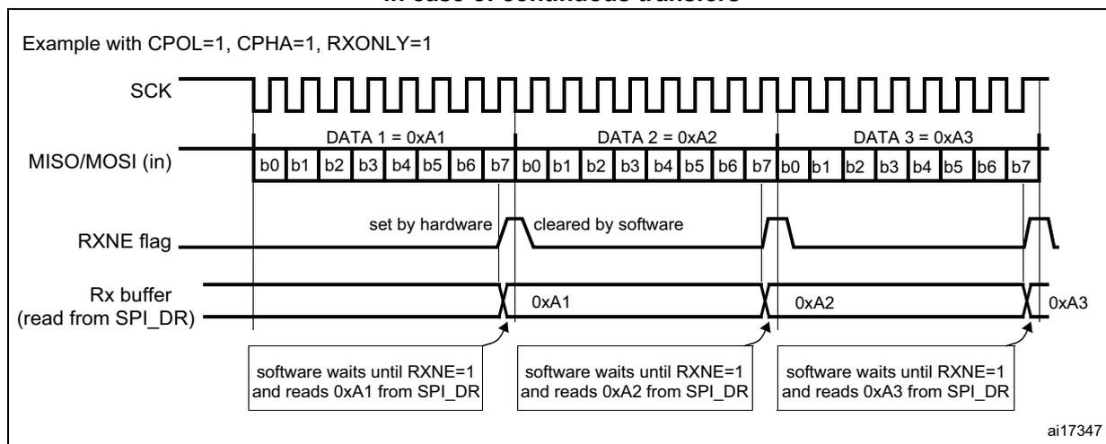
Example with CPOL=1, CPHA=1, RXONLY=1
The diagram shows the following signals and timing:
- SCK: A continuous square wave clock signal.
- MISO/MOSI (in): A data line showing three 8-bit data transfers: DATA 1 = 0xA1, DATA 2 = 0xA2, and DATA 3 = 0xA3. Each data item is shown as a sequence of bits b0 through b7.
- RXNE flag: The Receive Not Empty flag. It is set by hardware at the end of each data transfer (when the last bit b7 is received) and cleared by software when the data is read from the SPI_DR register.
- Rx buffer (read from SPI_DR): The receive buffer. It contains the received data: 0xA1, 0xA2, and 0xA3. The data is read by software when the RXNE flag is set.
- Software behavior: The software waits until the RXNE flag is set (RXNE=1) and then reads the data from the SPI_DR register. This process is repeated for each data transfer.
ai17347
Bidirectional receive procedure (BIDIMODE=1 and BIDIOE=0)
In this mode, the procedure is similar to the Receive-only mode procedure except that the BIDIMODE bit has to be set and the BIDIOE bit cleared in the SPI_CR2 register before enabling the SPI.
Continuous and discontinuous transfers
When transmitting data in master mode, if the software is fast enough to detect each rising edge of TXE (or TXE interrupt) and to immediately write to the SPI_DR register before the ongoing data transfer is complete, the communication is said to be continuous. In this case, there is no discontinuity in the generation of the SPI clock between each data item and the BSY bit is never cleared between each data transfer.
On the contrary, if the software is not fast enough, this can lead to some discontinuities in the communication. In this case, the BSY bit is cleared between each data transmission (see Figure 260 ).
In Master receive-only mode (RXONLY=1), the communication is always continuous and the BSY flag is always read at 1.
In slave mode, the continuity of the communication is decided by the SPI master device. In any case, even if the communication is continuous, the BSY flag goes low between each transfer for a minimum duration of one SPI clock cycle (see Figure 258 ).
Figure 260. TXE/BSY behavior when transmitting (BIDIRMODE=0 and RXONLY=0) in case of discontinuous transfers
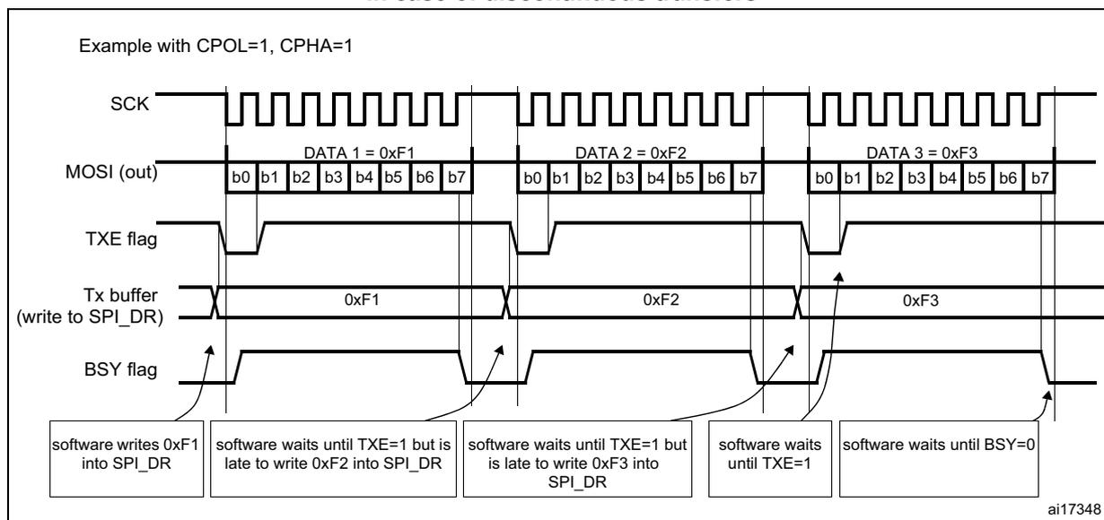
Example with CPOL=1, CPHA=1
The diagram illustrates the SPI transmission of three data bytes: DATA 1 = 0xF1, DATA 2 = 0xF2, and DATA 3 = 0xF3. Each byte is transmitted in 8 bits (b0 to b7). The SCK signal is a square wave. The MOSI (out) signal shows the data bits being transmitted. The TXE flag is set when the buffer is empty and ready for the next byte. The Tx buffer (write to SPI_DR) shows the data bytes being written. The BSY flag is set when the SPI is busy and reset when the SPI is idle. The diagram shows that the TXE flag is set when the buffer is empty, but it is not necessarily set when the buffer is full. The BSY flag is set when the SPI is busy, and it is reset when the SPI is idle.
software writes 0xF1 into SPI_DR
software waits until TXE=1 but is late to write 0xF2 into SPI_DR
software waits until TXE=1 but is late to write 0xF3 into SPI_DR
software waits until TXE=1
software waits until BSY=0
ai17348
25.3.6 CRC calculation
A CRC calculator has been implemented for communication reliability. Separate CRC calculators are implemented for transmitted data and received data. The CRC is calculated using a programmable polynomial serially on each bit. It is calculated on the sampling clock edge defined by the CPHA and CPOL bits in the SPI_CR1 register.
Note: This SPI offers two kinds of CRC calculation standard which depend directly on the data frame format selected for the transmission and/or reception: 8-bit data (CR8) and 16-bit data (CRC16).
CRC calculation is enabled by setting the CRCEN bit in the SPI_CR1 register. This action resets the CRC registers (SPI_RXCRCR and SPI_TXCRCR). In full duplex or transmitter only mode, when the transfers are managed by the software (CPU mode), it is necessary to write the bit CRCNEXT immediately after the last data to be transferred is written to the SPI_DR. At the end of this last data transfer, the SPI_TXCRCR value is transmitted.
In receive only mode and when the transfers are managed by software (CPU mode), it is necessary to write the CRCNEXT bit after the second last data has been received. The CRC is received just after the last data reception and the CRC check is then performed.
At the end of data and CRC transfers, the CRCERR flag in the SPI_SR register is set if corruption occurs during the transfer.
If data are present in the TX buffer, the CRC value is transmitted only after the transmission of the data byte. During CRC transmission, the CRC calculator is switched off and the register value remains unchanged.
SPI communication using the CRC is possible through the following procedure:
- 1. Program the CPOL, CPHA, LSBFirst, BR, SSM, SSI and MSTR values.
- 2. Program the polynomial in the SPI_CRCPR register.
- 3. Enable the CRC calculation by setting the CRCEN bit in the SPI_CR1 register. This also clears the SPI_RXCRCR and SPI_TXCRCR registers.
- 4. Enable the SPI by setting the SPE bit in the SPI_CR1 register.
- 5. Start the communication and sustain the communication until all but one byte or half-word have been transmitted or received.
- – In full duplex or transmitter-only mode, when the transfers are managed by software, when writing the last byte or half word to the Tx buffer, set the CRCNEXT bit in the SPI_CR1 register to indicate that the CRC is transmitted after the transmission of the last byte.
- – In receiver only mode, set the bit CRCNEXT just after the reception of the second to last data to prepare the SPI to enter in CRC Phase at the end of the reception of the last data. CRC calculation is frozen during the CRC transfer.
- 6. After the transfer of the last byte or half word, the SPI enters the CRC transfer and check phase. In full duplex mode or receiver-only mode, the received CRC is compared to the SPI_RXCRCR value. If the value does not match, the CRCERR flag in SPI_SR is set and an interrupt can be generated when the ERRIE bit in the SPI_CR2 register is set.
Note: When the SPI is in slave mode, be careful to enable CRC calculation only when the clock is stable, that is, when the clock is in the steady state. If not, a wrong CRC calculation may be done. In fact, the CRC is sensitive to the SCK slave input clock as soon as CRCEN is set, and this, whatever the value of the SPE bit.
With high bitrate frequencies, be careful when transmitting the CRC. As the number of used CPU cycles has to be as low as possible in the CRC transfer phase, it is forbidden to call software functions in the CRC transmission sequence to avoid errors in the last data and CRC reception. In fact, CRCNEXT bit has to be written before the end of the transmission/reception of the last data.
For high bit rate frequencies, it is advised to use the DMA mode to avoid the degradation of the SPI speed performance due to CPU accesses impacting the SPI bandwidth.
When the devices are configured as slaves and the NSS hardware mode is used, the NSS pin needs to be kept low between the data phase and the CRC phase.
When the SPI is configured in slave mode with the CRC feature enabled, CRC calculation takes place even if a high level is applied on the NSS pin. This may happen for example in case of a multislave environment where the communication master addresses slaves alternately.
Between a slave deselection (high level on NSS) and a new slave selection (low level on NSS), the CRC value should be cleared on both master and slave sides in order to resynchronize the master and slave for their respective CRC calculation.
To clear the CRC, follow the procedure below:
- 1. Disable SPI (SPE = 0)
- 2. Clear the CRCEN bit
- 3. Set the CRCEN bit
- 4. Enable the SPI (SPE = 1)
25.3.7 Status flags
Four status flags are provided for the application to completely monitor the state of the SPI bus.
Tx buffer empty flag (TXE)
When it is set, this flag indicates that the Tx buffer is empty and the next data to be transmitted can be loaded into the buffer. The TXE flag is cleared when writing to the SPI_DR register.
Rx buffer not empty (RXNE)
When set, this flag indicates that there are valid received data in the Rx buffer. It is cleared when SPI_DR is read.
BUSY flag
This BSY flag is set and cleared by hardware (writing to this flag has no effect). The BSY flag indicates the state of the communication layer of the SPI.
When BSY is set, it indicates that the SPI is busy communicating. There is one exception in master mode / bidirectional receive mode (MSTR=1 and BDM=1 and BDOE=0) where the BSY flag is kept low during reception.
The BSY flag is useful to detect the end of a transfer if the software wants to disable the SPI and enter Halt mode (or disable the peripheral clock). This avoids corrupting the last transfer. For this, the procedure described below must be strictly respected.
The BSY flag is also useful to avoid write collisions in a multimaster system.
The BSY flag is set when a transfer starts, with the exception of master mode / bidirectional receive mode (MSTR=1 and BDM=1 and BDOE=0).
It is cleared:
- • when a transfer is finished (except in master mode if the communication is continuous)
- • when the SPI is disabled
- • when a master mode fault occurs (MODF=1)
When communication is not continuous, the BSY flag is low between each communication.
When communication is continuous:
- • in master mode, the BSY flag is kept high during all the transfers
- • in slave mode, the BSY flag goes low for one SPI clock cycle between each transfer
Note: Do not use the BSY flag to handle each data transmission or reception. It is better to use the TXE and RXNE flags instead.
25.3.8 Disabling the SPI
When a transfer is terminated, the application can stop the communication by disabling the SPI peripheral. This is done by clearing the SPE bit.
For some configurations, disabling the SPI and entering the Halt mode while a transfer is ongoing can cause the current transfer to be corrupted and/or the BSY flag might become unreliable.
To avoid any of those effects, it is recommended to respect the following procedure when disabling the SPI:
In master or slave full-duplex mode (BIDIMODE=0, RXONLY=0)
- 1. Wait until RXNE=1 to receive the last data
- 2. Wait until TXE=1
- 3. Then wait until BSY=0
- 4. Disable the SPI (SPE=0) and, eventually, enter the Halt mode (or disable the peripheral clock)
In master or slave unidirectional transmit-only mode (BIDIMODE=0, RXONLY=0) or bidirectional transmit mode (BIDIMODE=1, BIDIOE=1)
After the last data is written into the SPI_DR register:
- 1. Wait until TXE=1
- 2. Then wait until BSY=0
- 3. Disable the SPI (SPE=0) and, eventually, enter the Halt mode (or disable the peripheral clock)
In master unidirectional receive-only mode (MSTR=1, BIDIMODE=0, RXONLY=1) or bidirectional receive mode (MSTR=1, BIDIMODE=1, BIDIOE=0)
This case must be managed in a particular way to ensure that the SPI does not initiate a new transfer. The sequence below is valid only for SPI Motorola configuration (FRF bit set to 0):
- 1. Wait for the second to last occurrence of RXNE=1 (n-1)
- 2. Then wait for one SPI clock cycle (using a software loop) before disabling the SPI (SPE=0)
- 3. Then wait for the last RXNE=1 before entering the Halt mode (or disabling the peripheral clock)
When the SPI is configured in TI mode (Bit FRF set to 1), the following procedure has to be respected to avoid generating an undesired pulse on NSS when the SPI is disabled:
- 1. Wait for the second to last occurrence of RXNE = 1 (n-1).
- 2. Disable the SPI (SPE = 0) in the following window frame using a software loop:
- – After at least one SPI clock cycle,
- – Before the beginning of the LSB data transfer.
Note: In master bidirectional receive mode (MSTR=1 and BDM=1 and BDOE=0), the BSY flag is kept low during transfers.
In slave receive-only mode (MSTR=0, BIDIMODE=0, RXONLY=1) or bidirectional receive mode (MSTR=0, BIDIMODE=1, BIDIOE=0)
- 1. You can disable the SPI (write SPE=1) at any time: the current transfer completes before the SPI is effectively disabled
- 2. Then, if you want to enter the Halt mode, you must first wait until BSY = 0 before entering the Halt mode (or disabling the peripheral clock).
25.3.9 SPI communication using DMA (direct memory addressing)
To operate at its maximum speed, the SPI needs to be fed with the data for transmission and the data received on the Rx buffer should be read to avoid overrun. To facilitate the
transfers, the SPI features a DMA capability implementing a simple request/acknowledge protocol.
A DMA access is requested when the enable bit in the SPI_CR2 register is enabled. Separate requests must be issued to the Tx and Rx buffers (see Figure 261 and Figure 262 ):
- • In transmission, a DMA request is issued each time TXE is set to 1. The DMA then writes to the SPI_DR register (this clears the TXE flag).
- • In reception, a DMA request is issued each time RXNE is set to 1. The DMA then reads the SPI_DR register (this clears the RXNE flag).
When the SPI is used only to transmit data, it is possible to enable only the SPI Tx DMA channel. In this case, the OVR flag is set because the data received are not read.
When the SPI is used only to receive data, it is possible to enable only the SPI Rx DMA channel.
In transmission mode, when the DMA has written all the data to be transmitted (flag TCIF is set in the DMA_ISR register), the BSY flag can be monitored to ensure that the SPI communication is complete. This is required to avoid corrupting the last transmission before disabling the SPI or entering the Stop mode. The software must first wait until TXE=1 and then until BSY=0.
Note: During discontinuous communications, there is a 2 APB clock period delay between the write operation to SPI_DR and the BSY bit setting. As a consequence, it is mandatory to wait first until TXE=1 and then until BSY=0 after writing the last data.
Figure 261. Transmission using DMA
Example with CPOL=1, CPHA=1
The diagram illustrates the timing and sequence of events for SPI transmission using DMA. The top section shows the SCK signal and the MISO/MOSI (out) data lines. The data is transmitted in 8-bit bytes (b0 to b7) for three data items: DATA 1 = 0xF1, DATA 2 = 0xF2, and DATA 3 = 0xF3. The TXE flag is set by hardware when the Tx buffer is empty and cleared by DMA write. The BSY flag is set by hardware when the SPI is active and reset by hardware when the SPI is inactive. The DMA request is ignored by the DMA because the DMA transfer is complete. The DMA TCIF flag is set by hardware when the DMA transfer is complete and clear by software. The software configures the DMA SPI Tx channel to send 3 data items and enables the SPI. The software waits until TXE=1 and then until BSY=0.
Sequence of events:
- software configures the DMA SPI Tx channel to send 3 data items and enables the SPI
- DMA writes DATA1 into SPI_DR
- DMA writes DATA2 into SPI_DR
- DMA writes DATA3 into SPI_DR
- DMA transfer is complete (TCIF=1 in DMA_ISR)
- software waits until TXE=1
- software waits until BSY=0
ai17349
Figure 262. Reception using DMA
Example with CPOL=1, CPHA=1
The diagram illustrates the timing for SPI reception using DMA. It shows the SCK signal, the MISO/MOSI (in) signal, the RXNE flag, the DMA request, the Rx buffer (read from SPI_DR), the DMA read from SPI_DR, and the flag DMA TCIF (DMA transfer complete). The example shows three data items: DATA 1 = 0xA1, DATA 2 = 0xA2, and DATA 3 = 0xA3. Each data item is 8 bits (b0-b7). The RXNE flag is set by hardware when the first bit is received and cleared by a DMA read. The DMA request is generated when the RXNE flag is set. The Rx buffer is updated with the received data. The DMA read from SPI_DR is performed by the DMA controller. The flag DMA TCIF is set by hardware when the last data item is received and cleared by software.
ai17350
DMA capability with CRC
When SPI communication is enabled with CRC communication and DMA mode, the transmission and reception of the CRC at the end of communication are automatic that is without using the bit CRCNEXT. After the CRC reception, the CRC must be read in the SPI_DR register to clear the RXNE flag.
At the end of data and CRC transfers, the CRCERR flag in SPI_SR is set if corruption occurs during the transfer.
25.3.10 Error flags
Master mode fault (MODF)
Master mode fault occurs when the master device has its NSS pin pulled low (in NSS hardware mode) or SSI bit low (in NSS software mode), this automatically sets the MODF bit. Master mode fault affects the SPI peripheral in the following ways:
- • The MODF bit is set and an SPI interrupt is generated if the ERRIE bit is set.
- • The SPE bit is cleared. This blocks all output from the device and disables the SPI interface.
- • The MSTR bit is cleared, thus forcing the device into slave mode.
Use the following software sequence to clear the MODF bit:
- 1. Make a read or write access to the SPI_SR register while the MODF bit is set.
- 2. Then write to the SPI_CR1 register.
To avoid any multiple slave conflicts in a system comprising several MCUs, the NSS pin must be pulled high during the MODF bit clearing sequence. The SPE and MSTR bits can be restored to their original state after this clearing sequence.
As a security, hardware does not allow the setting of the SPE and MSTR bits while the MODF bit is set.
In a slave device the MODF bit cannot be set. However, in a multimaster configuration, the device can be in slave mode with this MODF bit set. In this case, the MODF bit indicates that there might have been a multimaster conflict for system control. An interrupt routine can be used to recover cleanly from this state by performing a reset or returning to a default state.
Overrun condition
An overrun condition occurs when the master device has sent data bytes and the slave device has not cleared the RXNE bit resulting from the previous data byte transmitted. When an overrun condition occurs:
- • the OVR bit is set and an interrupt is generated if the ERRIE bit is set.
In this case, the receiver buffer contents are not updated with the newly received data from the master device. A read from the SPI_DR register returns this byte. All other subsequently transmitted bytes are lost.
Clearing the OVR bit is done by a read from the SPI_DR register followed by a read access to the SPI_SR register.
CRC error
This flag is used to verify the validity of the value received when the CRCEN bit in the SPI_CR1 register is set. The CRCERR flag in the SPI_SR register is set if the value received in the shift register does not match the receiver SPI_RXCRCR value.
TI mode frame format error
A TI mode frame format error is detected when an NSS pulse occurs during an ongoing communication when the SPI is acting in slave mode and configured to conform to the TI mode protocol. When this error occurs, the TIFRFE flag is set in the SPI_SR register. The SPI is not disabled when an error occurs, the NSS pulse is ignored, and the SPI waits for the next NSS pulse before starting a new transfer. The data may be corrupted since the error detection may result in the lost of two data bytes.
The TIFRFE flag is cleared when SPI_SR register is read. If the bit ERRIE is set, an interrupt is generated on the NSS error detection. In this case, the SPI should be disabled because data consistency is no more guaranteed and communications should be reinitiated by the master when the slave SPI is re-enabled.
Figure 263. TI mode frame format error detection
25.3.11 SPI interrupts
Table 99. SPI interrupt requests
| Interrupt event | Event flag | Enable Control bit |
|---|---|---|
| Transmit buffer empty flag | TXE | TXEIE |
| Receive buffer not empty flag | RXNE | RXNEIE |
| Master mode fault event | MODF | ERRIE |
| Overrun error | OVR | |
| CRC error flag | CRCERR | |
| TI frame format error | TIFRFE | ERRIE |
25.4 I 2 S functional description
25.4.1 I 2 S general description
The block diagram of the I 2 S is shown in Figure 264.
Figure 264. I 2 S block diagram
![Figure 264. I2S block diagram. This is a complex block diagram of the I2S interface. At the top, an 'Address and data bus' is shown. Below it, a 'Tx buffer' (16-bit) and an 'Rx buffer' (16-bit) are connected to a 'Shift register' (16-bit). The shift register is connected to 'MOSI/SD' and 'MISO' pins. A 'Communication control' block is connected to the buffers and the shift register, with various status flags: BSY, OVR, MODF, CRC ERR, UDR, CH SIDE, TxE, and RxNE. Below the communication control is a 'Master control logic' block. To its right are several configuration registers: I2SCFG [1:0], I2SSTD [1:0], CK POL, DATLEN [1:0], CH LEN, I2S MOD, and I2S EN. Below these are more registers: Bidi mode, Bidi OE, CRC EN, CRC Next, DFF, Rx only, SSM, and SSI. Further down are registers for LSB First, SPE, BR2, BR1, BR0, MSTR, CPOL, and CPHA. A 'SPI baud rate generator' is connected to the master control logic and the CK pin. Below it is an 'I2S clock generator' block, which receives inputs from 'MCK', 'I2SMOD', and 'I2SDIV[7:0]'. The I2S clock generator outputs 'I2SxCLK' to the CK pin. The CK pin is also connected to 'NSS/WS' and 'MCK' pins. The diagram is labeled 'ai14748' in the bottom right corner.](/RM0033-STM32F205-207-215-217/6fbae9cc09a7f0788bec9102a42d7559_img.jpg)
The SPI could function as an audio I 2 S interface when the I 2 S capability is enabled (by setting the I2SMOD bit in the SPI_I2SCFGR register). This interface uses almost the same pins, flags and interrupts as the SPI.
The I 2 S shares three common pins with the SPI:
- • SD: Serial Data (mapped on the MOSI pin) to transmit or receive the two time-multiplexed data channels (in half-duplex mode only).
- • WS: Word Select (mapped on the NSS pin) is the data control signal output in master mode and input in slave mode.
- • CK: Serial Clock (mapped on the SCK pin) is the serial clock output in master mode and serial clock input in slave mode.
An additional pin could be used when a master clock output is needed for some external audio devices:
- • MCK: Master Clock (mapped separately) is used, when the I 2 S is configured in master mode (and when the MCKOE bit in the SPI_I2SPR register is set), to output this additional clock generated at a preconfigured frequency rate equal to \( 256 \times F_S \) , where \( F_S \) is the audio sampling frequency.
The I 2 S uses its own clock generator to produce the communication clock when it is set in master mode. This clock generator is also the source of the master clock output. Two additional registers are available in I 2 S mode. One is linked to the clock generator configuration SPI_I2SPR and the other one is a generic I 2 S configuration register SPI_I2SCFGR (audio standard, slave/master mode, data format, packet frame, clock polarity, etc.).
The SPI_CR1 register and all CRC registers are not used in the I 2 S mode. Likewise, the SSOE bit in the SPI_CR2 register and the MODF and CRCERR bits in the SPI_SR are not used.
The I 2 S uses the same SPI register for data transfer (SPI_DR) in 16-bit wide mode.
25.4.2 Supported audio protocols
The three-line bus has to handle only audio data generally time-multiplexed on two channels: the right channel and the left channel. However there is only one 16-bit register for the transmission and the reception. So, it is up to the software to write into the data register the adequate value corresponding to the considered channel side, or to read the data from the data register and to identify the corresponding channel by checking the CHSIDE bit in the SPI_SR register. Channel Left is always sent first followed by the channel right (CHSIDE has no meaning for the PCM protocol).
Four data and packet frames are available. Data may be sent with a format of:
- • 16-bit data packed in 16-bit frame
- • 16-bit data packed in 32-bit frame
- • 24-bit data packed in 32-bit frame
- • 32-bit data packed in 32-bit frame
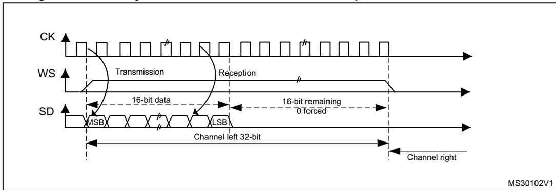
When using 16-bit data extended on 32-bit packet, the first 16 bits (MSB) are the significant bits, the 16-bit LSB is forced to 0 without any need for software action or DMA request (only one read/write operation).
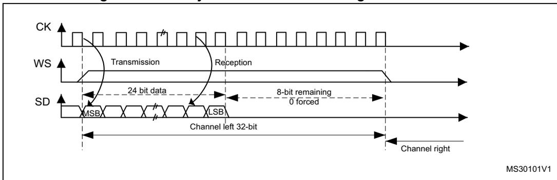
The 24-bit and 32-bit data frames need two CPU read or write operations to/from the SPI_DR or two DMA operations if the DMA is preferred for the application. For 24-bit data frame specifically, the 8 nonsignificant bits are extended to 32 bits with 0-bits (by hardware).
For all data formats and communication standards, the most significant bit is always sent first (MSB first).
The I 2 S interface supports four audio standards, configurable using the I2SSTD[1:0] and PCMSYNC bits in the SPI_I2SCFGR register.
I 2 S Philips standard
For this standard, the WS signal is used to indicate which channel is being transmitted. It is activated one CK clock cycle before the first bit (MSB) is available.
Figure 265. I 2 S Philips protocol waveforms (16/32-bit full accuracy, CPOL = 0)
Data are latched on the falling edge of CK (for the transmitter) and are read on the rising edge (for the receiver). The WS signal is also latched on the falling edge of CK.
Figure 266. I 2 S Philips standard waveforms (24-bit frame with CPOL = 0)
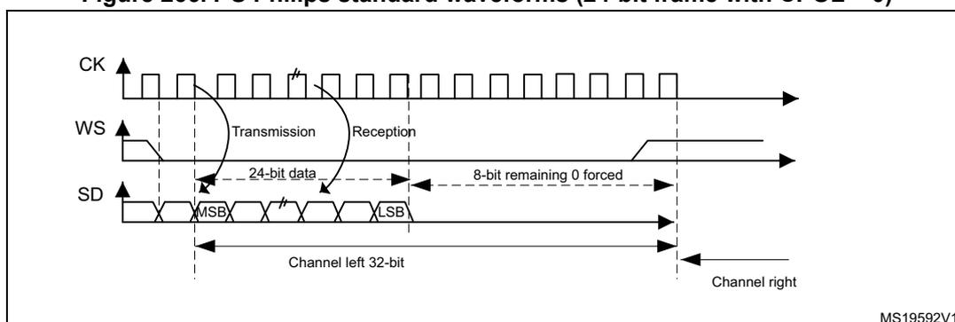
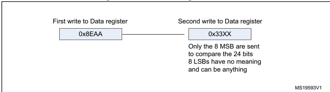
This mode needs two write or read operations to/from the SPI_DR.
- • In transmission mode:
if 0x8EAA33 has to be sent (24-bit):
Figure 267. Transmitting 0x8EAA33
- • In reception mode:
if data 0x8EAA33 is received:
Figure 268. Receiving 0x8EAA33
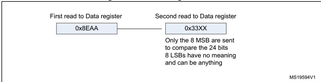
Figure 269. I 2 S Philips standard (16-bit extended to 32-bit packet frame with CPOL = 0)
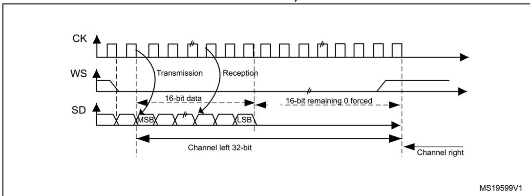
When 16-bit data frame extended to 32-bit channel frame is selected during the I 2 S configuration phase, only one access to SPI_DR is required. The 16 remaining bits are forced by hardware to 0x0000 to extend the data to 32-bit format.
If the data to transmit or the received data are 0x76A3 (0x76A30000 extended to 32-bit), the operation shown in Figure 270 is required.
Figure 270. Example
For transmission, each time an MSB is written to SPI_DR, the TXE flag is set and its interrupt, if allowed, is generated to load SPI_DR with the new value to send. This takes place even if 0x0000 have not yet been sent because it is done by hardware.
For reception, the RXNE flag is set and its interrupt, if allowed, is generated when the first 16 MSB half-word is received.
In this way, more time is provided between two write or read operations, which prevents underrun or overrun conditions (depending on the direction of the data transfer).
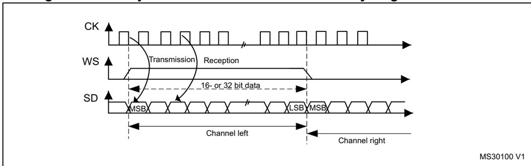
MSB justified standard
For this standard, the WS signal is generated at the same time as the first data bit, which is the MSB.
Figure 271. MSB justified 16-bit or 32-bit full-accuracy length with CPOL = 0
MS30100 V1
Data are latched on the falling edge of CK (for transmitter) and are read on the rising edge (for the receiver).
Figure 272. MSB justified 24-bit frame length with CPOL = 0
MS30101V1
Figure 273. MSB justified 16-bit extended to 32-bit packet frame with CPOL = 0
LSB justified standard
This standard is similar to the MSB justified standard (no difference for the 16-bit and 32-bit full-accuracy frame formats).
Figure 274. LSB justified 16-bit or 32-bit full-accuracy with CPOL = 0
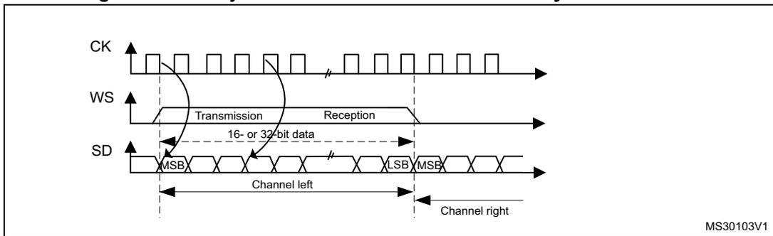
Figure 275. LSB justified 24-bit frame length with CPOL = 0
- • In transmission mode:
If data 0x3478AE have to be transmitted, two write operations to the SPI_DR register are required from software or by DMA. The operations are shown below.
Figure 276. Operations required to transmit 0x3478AE
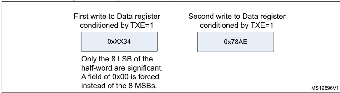
First write to Data register conditioned by TXE=1
0xXX34
Only the 8 LSB of the half-word are significant. A field of 0x00 is forced instead of the 8 MSBs.
Second write to Data register conditioned by TXE=1
0x78AE
MS19596V1
- • In reception mode:
If data 0x3478AE are received, two successive read operations from SPI_DR are required on each RXNE event.
Figure 277. Operations required to receive 0x3478AE
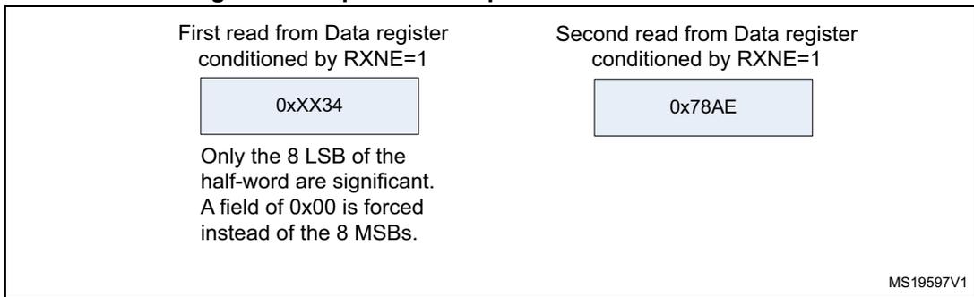
First read from Data register conditioned by RXNE=1
0xXX34
Only the 8 LSB of the half-word are significant. A field of 0x00 is forced instead of the 8 MSBs.
Second read from Data register conditioned by RXNE=1
0x78AE
MS19597V1
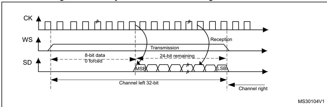
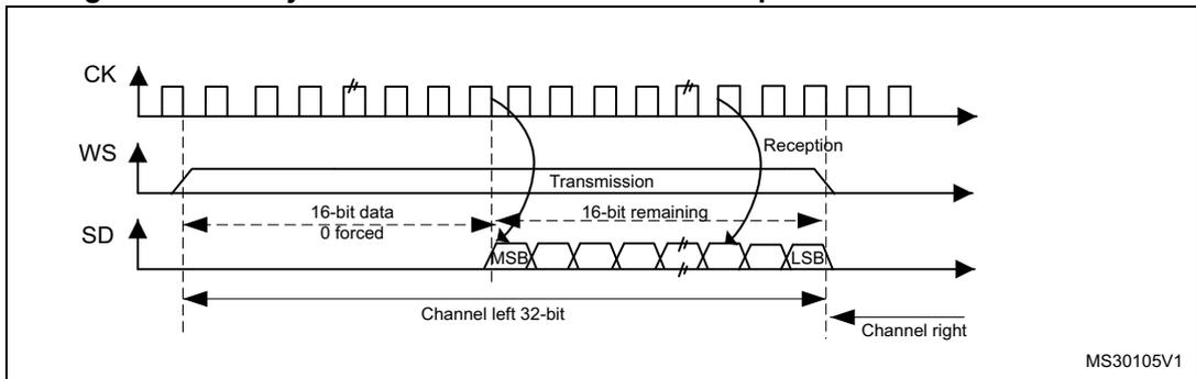
Figure 278. LSB justified 16-bit extended to 32-bit packet frame with CPOL = 0
CK
WS
SD
Transmission
Reception
16-bit data 0 forced
16-bit remaining
MSB
LSB
Channel left 32-bit
Channel right
MS30105V1
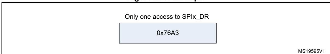
When 16-bit data frame extended to 32-bit channel frame is selected during the I 2 S configuration phase, Only one access to SPI_DR is required. The 16 remaining bits are forced by hardware to 0x0000 to extend the data to 32-bit format. In this case it corresponds to the half-word MSB.
If the data to transmit or the received data are 0x76A3 (0x0000 76A3 extended to 32-bit), the operation shown in Figure 279 is required.
Figure 279. Example of LSB justified 16-bit extended to 32-bit packet frame
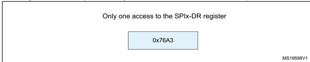
Only one access to the SPIx-DR register
0x76A3
MS19598V1
In transmission mode, when TXE is asserted, the application has to write the data to be transmitted (in this case 0x76A3). The 0x000 field is transmitted first (extension on 32-bit). TXE is asserted again as soon as the effective data (0x76A3) is sent on SD.
In reception mode, RXNE is asserted as soon as the significant half-word is received (and not the 0x0000 field).
In this way, more time is provided between two write or read operations to prevent underrun or overrun conditions.
PCM standard
For the PCM standard, there is no need to use channel-side information. The two PCM modes (short and long frame) are available and configurable using the PCMSYNC bit in SPI_I2SCFGR.
Figure 280. PCM standard waveforms (16-bit)
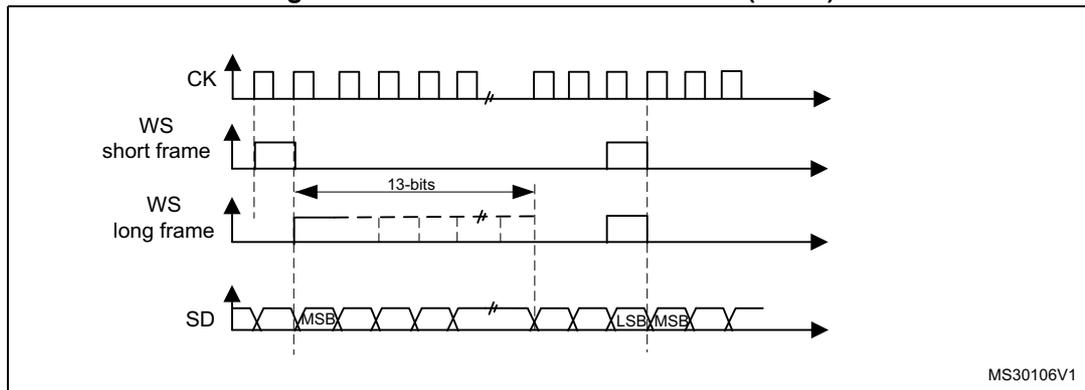
CK
WS short frame
WS long frame
SD
MSB
LSB
13-bits
MS30106V1
For long frame synchronization, the WS signal assertion time is fixed 13 bits in master mode.
For short frame synchronization, the WS synchronization signal is only one cycle long.
Figure 281. PCM standard waveforms (16-bit extended to 32-bit packet frame)
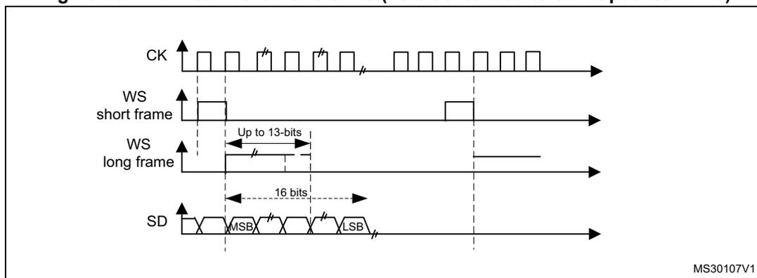
The diagram shows three signal lines: CK (clock), WS (word select), and SD (serial data). The CK line is a periodic square wave. The WS line is shown for two modes: 'short frame' and 'long frame'. In the short frame mode, the WS signal is a narrow pulse. In the long frame mode, the WS signal is a wider pulse. The SD line shows a sequence of bits, with the MSB (Most Significant Bit) and LSB (Least Significant Bit) marked. The diagram indicates that the number of bits between two consecutive pieces of data (and so two synchronization signals) can be up to 13 bits in short frame mode and 16 bits in long frame mode. The diagram is labeled MS30107V1.
Note: For both modes (master and slave) and for both synchronizations (short and long), the number of bits between two consecutive pieces of data (and so two synchronization signals) needs to be specified (DATLEN and CHLEN bits in the SPI_I2SCFGR register) even in slave mode.
25.4.3 Clock generator
The I 2 S bitrate determines the dataflow on the I 2 S data line and the I 2 S clock signal frequency.
I 2 S bitrate = number of bits per channel × number of channels × sampling audio frequency
For a 16-bit audio, left and right channel, the I 2 S bitrate is calculated as follows:
It is I 2 S bitrate = 32 × 2 × F S if the packet length is 32-bit wide.
Figure 282. Audio sampling frequency definition
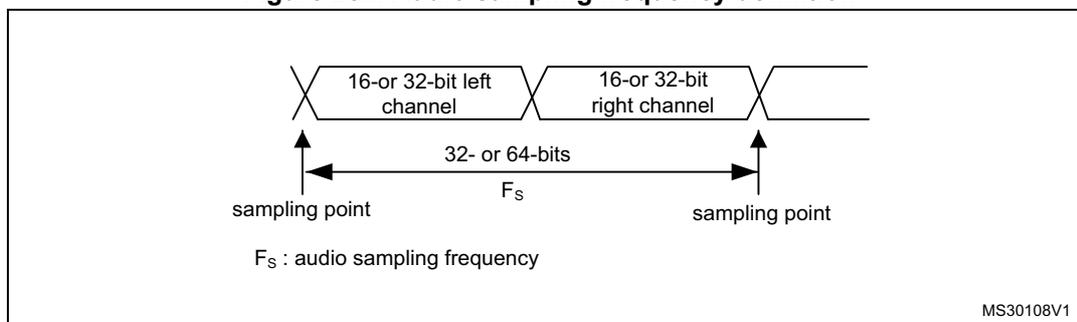
The diagram illustrates the audio sampling frequency (F S ). It shows two consecutive audio samples. Each sample consists of a '16- or 32-bit left channel' followed by a '16- or 32-bit right channel'. The time interval between the 'sampling point' of one sample and the 'sampling point' of the next sample is labeled F S . The total duration of one sample (left + right) is labeled '32- or 64-bits'. The diagram is labeled MS30108V1.
When the master mode is configured, a specific action needs to be taken to properly program the linear divider in order to communicate with the desired audio frequency.
Figure 283. I 2 S clock generator architecture![Figure 283. I2S clock generator architecture diagram. The diagram shows the internal logic for generating the I2S clock. An input I2SxCLK is connected to a '8-bit linear divider + reshaping stage'. This stage is controlled by a register with bits MCKOE, ODD, and I2SDIV[7:0]. The output of the divider goes to a 'Divider by 4', which then goes to a 'Div2' block. The output of Div2 is connected to a multiplexer (MUX) labeled '0' and '1'. The MUX is controlled by a register with bits I2SMOD and CHLEN. The output of the MUX is labeled CK. Another MUX labeled 'MCK' is also shown, with its output labeled MCK. The diagram is labeled MS30109V1 in the bottom right corner.](/RM0033-STM32F205-207-215-217/6ec198a5a264620200becfa498eee4c1_img.jpg)
- 1. Where x could be 2 or 3.
Figure 282 presents the communication clock architecture. To achieve high-quality audio performance, the I2SxCLK clock source can be either the PLLI2S output (through R division factor) or an external clock (mapped to I2S_CKIN pin).
The audio sampling frequency can be 96 kHz, 48 kHz, 44.1 kHz, 32 kHz, 22.05 kHz, 16 kHz, 11.025 kHz or 8 kHz (or any other value within this range). In order to reach the desired frequency, the linear divider needs to be programmed according to the formulas below:
When the master clock is generated (MCKOE in the SPI_I2SPR register is set):
When the master clock is disabled (MCKOE bit cleared):
Table 100 provides example precision values for different clock configurations.
Note: Other configurations are possible that allow optimum clock precision.
Table 100. Audio frequency precision (for PLLM VCO = 1 MHz or 2 MHz) (1)| Master clock | Target f s (Hz) | Data format | PLL12SN | PLL12SR | I2SDIV | I2SODD | Real f s (Hz) | Error |
|---|---|---|---|---|---|---|---|---|
| Disabled | 8000 | 16-bit | 192 | 2 | 187 | 1 | 8000 | 0.0000% |
| 32-bit | 192 | 3 | 62 | 1 | 8000 | 0.0000% | ||
| 16000 | 16-bit | 192 | 3 | 62 | 1 | 16000 | 0.0000% | |
| 32-bit | 256 | 2 | 62 | 1 | 16000 | 0.0000% | ||
| 32000 | 16-bit | 256 | 2 | 62 | 1 | 32000 | 0.0000% | |
| 32-bit | 256 | 5 | 12 | 1 | 32000 | 0.0000% | ||
| 48000 | 16-bit | 192 | 5 | 12 | 1 | 48000 | 0.0000% | |
| 32-bit | 384 | 5 | 12 | 1 | 48000 | 0.0000% | ||
| 96000 | 16-bit | 384 | 5 | 12 | 1 | 96000 | 0.0000% | |
| 32-bit | 424 | 3 | 11 | 1 | 96014.49219 | 0.0151% | ||
| 22050 | 16-bit | 290 | 3 | 68 | 1 | 22049.87695 | 0.0006% | |
| 32-bit | 302 | 2 | 53 | 1 | 22050.23438 | 0.0011% | ||
| 44100 | 16-bit | 302 | 2 | 53 | 1 | 44100.46875 | 0.0011% | |
| 32-bit | 429 | 4 | 19 | 0 | 44099.50781 | 0.0011% | ||
| 192000 | 16-bit | 424 | 3 | 11 | 1 | 192028.9844 | 0.0151% | |
| 32-bit | 258 | 3 | 3 | 1 | 191964.2813 | 0.0186% | ||
| Enabled | 8000 | don't care | 256 | 5 | 12 | 1 | 8000 | 0.0000% |
| 16000 | don't care | 213 | 2 | 13 | 0 | 16000.60059 | 0.0038% | |
| 32000 | don't care | 213 | 2 | 6 | 1 | 32001.20117 | 0.0038% | |
| 48000 | don't care | 258 | 3 | 3 | 1 | 47991.07031 | 0.0186% | |
| 96000 | don't care | 344 | 2 | 3 | 1 | 95982.14063 | 0.0186% | |
| 22050 | don't care | 429 | 4 | 9 | 1 | 22049.75391 | 0.0011% | |
| 44100 | don't care | 271 | 2 | 6 | 0 | 44108.07422 | 0.0183% |
1. This table gives only example values for different clock configurations. Other configurations allowing optimum clock precision are possible.
25.4.4 I 2 S master mode
The I 2 S can be configured in master mode for transmission and reception. This means that the serial clock is generated on the CK pin as well as the Word Select signal WS. Master clock (MCK) may be output or not, thanks to the MCKOE bit in the SPI_I2SPR register.
Procedure
- 1. Select the I2SDIV[7:0] bits in the SPI_I2SPR register to define the serial clock baud rate to reach the proper audio sample frequency. The ODD bit in the SPI_I2SPR register also has to be defined.
- 2. Select the CKPOL bit to define the steady level for the communication clock. Set the MCKOE bit in the SPI_I2SPR register if the master clock MCK needs to be provided to
the external DAC/ADC audio component (the I2SDIV and ODD values should be computed depending on the state of the MCK output, for more details refer to Section 25.4.3 ).
- 3. Set the I2SMOD bit in SPI_I2SCFGR to activate the I 2 S functionalities and choose the I 2 S standard through the I2SSTD[1:0] and PCMSYNC bits, the data length through the DATLEN[1:0] bits and the number of bits per channel by configuring the CHLEN bit. Select also the I 2 S master mode and direction (Transmitter or Receiver) through the I2SCFG[1:0] bits in the SPI_I2SCFGR register.
- 4. If needed, select all the potential interruption sources and the DMA capabilities by writing the SPI_CR2 register.
- 5. The I2SE bit in SPI_I2SCFGR register must be set.
WS and CK are configured in output mode. MCK is also an output, if the MCKOE bit in SPI_I2SPR is set.
Transmission sequence
The transmission sequence begins when a half-word is written into the Tx buffer.
Assumedly, the first data written into the Tx buffer correspond to the channel Left data. When data are transferred from the Tx buffer to the shift register, TXE is set and data corresponding to the channel Right have to be written into the Tx buffer. The CHSIDE flag indicates which channel is to be transmitted. It has a meaning when the TXE flag is set because the CHSIDE flag is updated when TXE goes high.
A full frame has to be considered as a Left channel data transmission followed by a Right channel data transmission. It is not possible to have a partial frame where only the left channel is sent.
The data half-word is parallel loaded into the 16-bit shift register during the first bit transmission, and then shifted out, serially, to the MOSI/SD pin, MSB first. The TXE flag is set after each transfer from the Tx buffer to the shift register and an interrupt is generated if the TXEIE bit in the SPI_CR2 register is set.
For more details about the write operations depending on the I 2 S standard mode selected, refer to Section 25.4.2 .
To ensure a continuous audio data transmission, it is mandatory to write the SPI_DR with the next data to transmit before the end of the current transmission.
To switch off the I 2 S, by clearing I2SE, it is mandatory to wait for TXE = 1 and BSY = 0.
Reception sequence
The operating mode is the same as for the transmission mode except for the point 3 (refer to the procedure described in Section 25.4.4 ), where the configuration should set the master reception mode through the I2SCFG[1:0] bits.
Whatever the data or channel length, the audio data are received by 16-bit packets. This means that each time the Rx buffer is full, the RXNE flag is set and an interrupt is generated if the RXNEIE bit is set in SPI_CR2 register. Depending on the data and channel length configuration, the audio value received for a right or left channel may result from one or two receptions into the Rx buffer.
Clearing the RXNE bit is performed by reading the SPI_DR register.
CHSIDE is updated after each reception. It is sensitive to the WS signal generated by the I 2 S cell.
For more details about the read operations depending on the I 2 S standard mode selected, refer to Section 25.4.2: Supported audio protocols .
If data are received while the previously received data have not been read yet, an overrun is generated and the OVR flag is set. If the ERRIE bit is set in the SPI_CR2 register, an interrupt is generated to indicate the error.
To switch off the I 2 S, specific actions are required to ensure that the I 2 S completes the transfer cycle properly without initiating a new data transfer. The sequence depends on the configuration of the data and channel lengths, and on the audio protocol mode selected. In the case of:
- • 16-bit data length extended on 32-bit channel length (DATLEN = 00 and CHLEN = 1) using the LSB justified mode (I2SSTD = 10)
- a) Wait for the second to last RXNE = 1 (n – 1)
- b) Then wait 17 I 2 S clock cycles (using a software loop)
- c) Disable the I 2 S (I2SE = 0)
- • 16-bit data length extended on 32-bit channel length (DATLEN = 00 and CHLEN = 1) in MSB justified, I
2
S or PCM modes (I2SSTD = 00, I2SSTD = 01 or I2SSTD = 11, respectively)
- a) Wait for the last RXNE
- b) Then wait 1 I 2 S clock cycle (using a software loop)
- c) Disable the I 2 S (I2SE = 0)
- • For all other combinations of DATLEN and CHLEN, whatever the audio mode selected through the I2SSTD bits, carry out the following sequence to switch off the I
2
S:
- a) Wait for the second to last RXNE = 1 (n – 1)
- b) Then wait one I 2 S clock cycle (using a software loop)
- c) Disable the I 2 S (I2SE = 0)
Note: The BSY flag is kept low during transfers.
25.4.5 I 2 S slave mode
In slave mode, the I 2 S can be configured in transmission or reception mode. The operating mode is following mainly the same rules as described for the I 2 S master configuration. In slave mode, there is no clock to be generated by the I 2 S interface. The clock and WS signals are input from the external master connected to the I 2 S interface. There is then no need, for the user, to configure the clock.
The configuration steps to follow are listed below:
- 1. Set the I2SMOD bit in the SPI_I2SCFGR register to reach the I 2 S functionalities and choose the I 2 S standard through the I2SSTD[1:0] bits, the data length through the DATLEN[1:0] bits and the number of bits per channel for the frame configuring the CHLEN bit. Select also the mode (transmission or reception) for the slave through the I2SCFG[1:0] bits in SPI_I2SCFGR register.
- 2. If needed, select all the potential interrupt sources and the DMA capabilities by writing the SPI_CR2 register.
- 3. The I2SE bit in SPI_I2SCFGR register must be set.
Transmission sequence
The transmission sequence begins when the external master device sends the clock and when the NSS_WS signal requests the transfer of data. The slave has to be enabled before the external master starts the communication. The I 2 S data register has to be loaded before the master initiates the communication.
For the I 2 S, MSB justified and LSB justified modes, the first data item to be written into the data register corresponds to the data for the left channel. When the communication starts, the data are transferred from the Tx buffer to the shift register. The TXE flag is then set in order to request the right channel data to be written into the I 2 S data register.
The CHSIDE flag indicates which channel is to be transmitted. Compared to the master transmission mode, in slave mode, CHSIDE is sensitive to the WS signal coming from the external master. This means that the slave needs to be ready to transmit the first data before the clock is generated by the master. WS assertion corresponds to left channel transmitted first.
Note: The I2SE has to be written at least two PCLK cycles before the first clock of the master comes on the CK line.
The data half-word is parallel-loaded into the 16-bit shift register (from the internal bus) during the first bit transmission, and then shifted out serially to the MOSI/SD pin MSB first. The TXE flag is set after each transfer from the Tx buffer to the shift register and an interrupt is generated if the TXEIE bit in the SPI_CR2 register is set.
Note that the TXE flag should be checked to be at 1 before attempting to write the Tx buffer.
For more details about the write operations depending on the I 2 S standard mode selected, refer to Section 25.4.2 .
To secure a continuous audio data transmission, it is mandatory to write the SPI_DR register with the next data to transmit before the end of the current transmission. An underrun flag is set and an interrupt may be generated if the data are not written into the SPI_DR register before the first clock edge of the next data communication. This indicates to the software that the transferred data are wrong. If the ERRIE bit is set into the SPI_CR2 register, an interrupt is generated when the UDR flag in the SPI_SR register goes high. In this case, it is mandatory to switch off the I 2 S and to restart a data transfer starting from the left channel.
To switch off the I 2 S, by clearing the I2SE bit, it is mandatory to wait for TXE = 1 and BSY = 0.
Reception sequence
The operating mode is the same as for the transmission mode except for the point 1 (refer to the procedure described in Section 25.4.5 ), where the configuration should set the master reception mode using the I2SCFG[1:0] bits in the SPI_I2SCFGR register.
Whatever the data length or the channel length, the audio data are received by 16-bit packets. This means that each time the RX buffer is full, the RXNE flag in the SPI_SR register is set and an interrupt is generated if the RXNEIE bit is set in the SPI_CR2 register. Depending on the data length and channel length configuration, the audio value received for a right or left channel may result from one or two receptions into the RX buffer.
The CHSIDE flag is updated each time data are received to be read from SPI_DR. It is sensitive to the external WS line managed by the external master component.
Clearing the RXNE bit is performed by reading the SPI_DR register.
For more details about the read operations depending the I 2 S standard mode selected, refer to Section 25.4.2 .
If data are received while the precedent received data have not yet been read, an overrun is generated and the OVR flag is set. If the bit ERRRIE is set in the SPI_CR2 register, an interrupt is generated to indicate the error.
To switch off the I 2 S in reception mode, I2SE has to be cleared immediately after receiving the last RXNE = 1.
Note: The external master components should have the capability of sending/receiving data in 16-bit or 32-bit packets via an audio channel.
25.4.6 Status flags
Three status flags are provided for the application to fully monitor the state of the I 2 S bus.
Busy flag (BSY)
The BSY flag is set and cleared by hardware (writing to this flag has no effect). It indicates the state of the communication layer of the I 2 S.
When BSY is set, it indicates that the I 2 S is busy communicating. There is one exception in master receive mode (I2SCFG = 11) where the BSY flag is kept low during reception.
The BSY flag is useful to detect the end of a transfer if the software needs to disable the I 2 S. This avoids corrupting the last transfer. For this, the procedure described below must be strictly respected.
The BSY flag is set when a transfer starts, except when the I 2 S is in master receiver mode.
The BSY flag is cleared:
- • when a transfer completes (except in master transmit mode, in which the communication is supposed to be continuous)
- • when the I 2 S is disabled
When communication is continuous:
- • In master transmit mode, the BSY flag is kept high during all the transfers
- • In slave mode, the BSY flag goes low for one I 2 S clock cycle between each transfer
Note: Do not use the BSY flag to handle each data transmission or reception. It is better to use the TXE and RXNE flags instead.
Tx buffer empty flag (TXE)
When set, this flag indicates that the Tx buffer is empty and the next data to be transmitted can then be loaded into it. The TXE flag is reset when the Tx buffer already contains data to be transmitted. It is also reset when the I 2 S is disabled (I2SE bit is reset).
RX buffer not empty (RXNE)
When set, this flag indicates that there are valid received data in the RX Buffer. It is reset when SPI_DR register is read.
Channel Side flag (CHSIDE)
In transmission mode, this flag is refreshed when TXE goes high. It indicates the channel side to which the data to transfer on SD has to belong. In case of an underrun error event in
slave transmission mode, this flag is not reliable and I 2 S needs to be switched off and switched on before resuming the communication.
In reception mode, this flag is refreshed when data are received into SPI_DR. It indicates from which channel side data have been received. Note that in case of error (like OVR) this flag becomes meaningless and the I 2 S should be reset by disabling and then enabling it (with configuration if it needs changing).
This flag has no meaning in the PCM standard (for both Short and Long frame modes).
When the OVR or UDR flag in the SPI_SR is set and the ERRIE bit in SPI_CR2 is also set, an interrupt is generated. This interrupt can be cleared by reading the SPI_SR status register (once the interrupt source has been cleared).
25.4.7 Error flags
There are two error flags for the I 2 S cell.
Underrun flag (UDR)
In slave transmission mode this flag is set when the first clock for data transmission appears while the software has not yet loaded any value into SPI_DR. It is available when the I2SMOD bit in SPI_I2SCFGR is set. An interrupt may be generated if the ERRIE bit in SPI_CR2 is set.
The UDR bit is cleared by a read operation on the SPI_SR register.
Overrun flag (OVR)
This flag is set when data are received and the previous data have not yet been read from SPI_DR. As a result, the incoming data are lost. An interrupt may be generated if the ERRIE bit is set in SPI_CR2.
In this case, the receive buffer contents are not updated with the newly received data from the transmitter device. A read operation to the SPI_DR register returns the previous correctly received data. All other subsequently transmitted half-words are lost.
Clearing the OVR bit is done by a read operation on the SPI_DR register followed by a read access to the SPI_SR register.
25.4.8 I 2 S interrupts
Table 101 provides the list of I 2 S interrupts.
Table 101. I 2 S interrupt requests
| Interrupt event | Event flag | Enable Control bit |
|---|---|---|
| Transmit buffer empty flag | TXE | TXEIE |
| Receive buffer not empty flag | RXNE | RXNEIE |
| Overrun error | OVR | ERRIE |
| Underrun error | UDR |
DMA is working in exactly the same way as for the SPI mode. There is no difference on the I 2 S. Only the CRC feature is not available in I 2 S mode since there is no data transfer protection system.
25.5 SPI and I 2 S registers
The peripheral registers must be accessed by half-words (16 bits) or words (32 bits).
25.5.1 SPI control register 1 (SPI_CR1) (not used in I 2 S mode)
Address offset: 0x00
Reset value: 0x0000
| 15 | 14 | 13 | 12 | 11 | 10 | 9 | 8 | 7 | 6 | 5 | 4 | 3 | 2 | 1 | 0 |
|---|---|---|---|---|---|---|---|---|---|---|---|---|---|---|---|
| BIDI MODE | BIDI OE | CRC EN | CRC NEXT | DFF | RX ONLY | SSM | SSI | LSB FIRST | SPE | BR [2:0] | MSTR | CPOL | CPHA | ||
| rw | rw | rw | rw | rw | rw | rw | rw | rw | rw | rw | rw | rw | rw | rw | rw |
Bit 15 BIDIMODE: Bidirectional data mode enable
0: 2-line unidirectional data mode selected
1: 1-line bidirectional data mode selected
Note: This bit is not used in I 2 S mode
Bit 14 BIDIOE: Output enable in bidirectional mode
This bit combined with the BIDImode bit selects the direction of transfer in bidirectional mode
0: Output disabled (receive-only mode)
1: Output enabled (transmit-only mode)
Note: This bit is not used in I 2 S mode.
In master mode, the MOSI pin is used while the MISO pin is used in slave mode.
Bit 13 CRCEN: Hardware CRC calculation enable
0: CRC calculation disabled
1: CRC calculation enabled
Note: This bit should be written only when SPI is disabled (SPE = '0') for correct operation.
It is not used in I 2 S mode.
Bit 12 CRCNEXT: CRC transfer next
0: Data phase (no CRC phase)
1: Next transfer is CRC (CRC phase)
Note: When the SPI is configured in full duplex or transmitter only modes, CRCNEXT must be written as soon as the last data is written to the SPI_DR register.
When the SPI is configured in receiver only mode, CRCNEXT must be set after the second last data reception.
This bit should be kept cleared when the transfers are managed by DMA.
It is not used in I 2 S mode.
Bit 11 DFF: Data frame format
0: 8-bit data frame format is selected for transmission/reception
1: 16-bit data frame format is selected for transmission/reception
Note: This bit should be written only when SPI is disabled (SPE = '0') for correct operation.
It is not used in I 2 S mode.
Bit 10 RXONLY: Receive onlyThis bit combined with the BIDImode bit selects the direction of transfer in 2-line unidirectional mode. This bit is also useful in a multislave system in which this particular slave is not accessed, the output from the accessed slave is not corrupted.
0: Full duplex (Transmit and receive)
1: Output disabled (Receive-only mode)
Note: This bit is not used in I 2 S mode
Bit 9 SSM: Software slave managementWhen the SSM bit is set, the NSS pin input is replaced with the value from the SSI bit.
0: Software slave management disabled
1: Software slave management enabled
Note: This bit is not used in I 2 S mode and SPI TI mode
Bit 8 SSI: Internal slave selectThis bit has an effect only when the SSM bit is set. The value of this bit is forced onto the NSS pin and the IO value of the NSS pin is ignored.
Note: This bit is not used in I 2 S mode and SPI TI mode
Bit 7 LSBFIRST: Frame format0: MSB transmitted first
1: LSB transmitted first
Note: This bit should not be changed when communication is ongoing.
It is not used in I 2 S mode and SPI TI mode
Bit 6 SPE: SPI enable0: Peripheral disabled
1: Peripheral enabled
Note: This bit is not used in I 2 S mode.
When disabling the SPI, follow the procedure described in Section 25.3.8 .
Bits 5:3 BR[2:0]: Baud rate control000: f PCLK /2
001: f PCLK /4
010: f PCLK /8
011: f PCLK /16
100: f PCLK /32
101: f PCLK /64
110: f PCLK /128
111: f PCLK /256
Note: These bits should not be changed when communication is ongoing.
They are not used in I 2 S mode.
Bit 2 MSTR: Master selection0: Slave configuration
1: Master configuration
Note: This bit should not be changed when communication is ongoing.
It is not used in I 2 S mode.
Bit 1 CPOL : Clock polarity
0: CK to 0 when idle
1: CK to 1 when idle
Note: This bit should not be changed when communication is ongoing.
It is not used in I 2 S mode and SPI TI mode.
Bit 0 CPHA : Clock phase
0: The first clock transition is the first data capture edge
1: The second clock transition is the first data capture edge
Note: This bit should not be changed when communication is ongoing.
It is not used in I 2 S mode and SPI TI mode.
25.5.2 SPI control register 2 (SPI_CR2)
Address offset: 0x04
Reset value: 0x0000
| 15 | 14 | 13 | 12 | 11 | 10 | 9 | 8 | 7 | 6 | 5 | 4 | 3 | 2 | 1 | 0 |
|---|---|---|---|---|---|---|---|---|---|---|---|---|---|---|---|
| Reserved | TXEIE | RXNEIE | ERRIE | FRF | Res. | SSOE | TXDMAEN | RXDMAEN | |||||||
| rw | rw | rw | rw | rw | rw | rw | |||||||||
Bits 15:8 Reserved, must be kept at reset value.
Bit 7 TXEIE : Tx buffer empty interrupt enable
0: TXE interrupt masked
1: TXE interrupt not masked. Used to generate an interrupt request when the TXE flag is set.
Bit 6 RXNEIE : RX buffer not empty interrupt enable
0: RXNE interrupt masked
1: RXNE interrupt not masked. Used to generate an interrupt request when the RXNE flag is set.
Bit 5 ERRIE : Error interrupt enable
This bit controls the generation of an interrupt when an error condition occurs (UDR, OVR in I 2 S mode)(CRCERR, OVR, MODF in SPI mode, FRE in TI mode and UDR, OVR, and FRE in I 2 S mode).
0: Error interrupt is masked
1: Error interrupt is enabled
Bit 4 FRF : Frame format
0: SPI Motorola mode
1: SPI TI mode
Note: This bit is not used in I 2 S mode.
Bit 3 Reserved. Forced to 0 by hardware.
Bit 2 SSOE : SS output enable
0: SS output is disabled in master mode and the cell can work in multimaster configuration
1: SS output is enabled in master mode and when the cell is enabled. The cell cannot work in a multimaster environment.
Note: This bit is not used in I 2 S mode and SPI TI mode.
Bit 1 TXDMAEN : Tx buffer DMA enable
When this bit is set, the DMA request is made whenever the TXE flag is set.
0: Tx buffer DMA disabled
1: Tx buffer DMA enabled
Bit 0 RXDMAEN : Rx buffer DMA enable
When this bit is set, the DMA request is made whenever the RXNE flag is set.
0: Rx buffer DMA disabled
1: Rx buffer DMA enabled
25.5.3 SPI status register (SPI_SR)
Address offset: 0x08
Reset value: 0x0002
| 15 | 14 | 13 | 12 | 11 | 10 | 9 | 8 | 7 | 6 | 5 | 4 | 3 | 2 | 1 | 0 |
|---|---|---|---|---|---|---|---|---|---|---|---|---|---|---|---|
| Reserved | TIFRFE | BSY | OVR | MODF | CRC ERR | UDR | CHSIDE | TXE | RXNE | ||||||
| r | r | r | r | r | rc_w0 | r | r | r | r | ||||||
Bits 15:9 Reserved. Forced to 0 by hardware.
Bit 8 TIFRFE : TI frame format error
0: No frame format error
1: A frame format error occurred
Bit 7 BSY : Busy flag
0: SPI (or I2S) not busy
1: SPI (or I2S) is busy in communication or Tx buffer is not empty
This flag is set and cleared by hardware.
Note: BSY flag must be used with caution: refer to Section 25.3.7 and Section 25.3.8.
Bit 6 OVR : Overrun flag
0: No overrun occurred
1: Overrun occurred
This flag is set by hardware and reset by a software sequence (see Section 25.3.10).
Bit 5 MODF : Mode fault
0: No mode fault occurred
1: Mode fault occurred
This flag is set by hardware and reset by a software sequence (see Section 25.3.10).
Note: This bit is not used in I 2 S mode
Bit 4 CRCCERR : CRC error flag
0: CRC value received matches the SPI_RXCRCR value
1: CRC value received does not match the SPI_RXCRCR value
This flag is set by hardware and cleared by software writing 0.
Note: This bit is not used in I 2 S mode.
Bit 3 UDR : Underrun flag
0: No underrun occurred
1: Underrun occurred
This flag is set by hardware and reset by a software sequence. Refer to Section 25.4.7: Error flags for the software sequence.
Note: This bit is not used in SPI mode.
Bit 2 CHSIDE : Channel side
0: Channel Left has to be transmitted or has been received
1: Channel Right has to be transmitted or has been received
Note: This bit is not used for SPI mode and is meaningless in PCM mode.
Bit 1 TXE : Transmit buffer empty
0: Tx buffer not empty
1: Tx buffer empty
Bit 0 RXNE : Receive buffer not empty
0: Rx buffer empty
1: Rx buffer not empty
25.5.4 SPI data register (SPI_DR)
Address offset: 0x0C
Reset value: 0x0000

| 15 | 14 | 13 | 12 | 11 | 10 | 9 | 8 | 7 | 6 | 5 | 4 | 3 | 2 | 1 | 0 |
| DR[15:0] | |||||||||||||||
| rw | rw | rw | rw | rw | rw | rw | rw | rw | rw | rw | rw | rw | rw | rw | rw |
Bits 15:0 DR[15:0] : Data register
Data received or to be transmitted.
The data register is split into 2 buffers - one for writing (Transmit Buffer) and another one for reading (Receive buffer). A write to the data register writes into the Tx buffer and a read from the data register returns the value held in the Rx buffer.
Note: These notes apply to SPI mode:
Depending on the data frame format selection bit (DFF in SPI_CR1 register), the data sent or received is either 8-bit or 16-bit. This selection has to be made before enabling the SPI to ensure correct operation.
For an 8-bit data frame, the buffers are 8-bit and only the LSB of the register (SPI_DR[7:0]) is used for transmission/reception. When in reception mode, the MSB of the register (SPI_DR[15:8]) is forced to 0.
For a 16-bit data frame, the buffers are 16-bit and the entire register, SPI_DR[15:0] is used for transmission/reception.
25.5.5 SPI CRC polynomial register (SPI_CRCPR) (not used in I 2 S mode)
Address offset: 0x10
Reset value: 0x0007

| 15 | 14 | 13 | 12 | 11 | 10 | 9 | 8 | 7 | 6 | 5 | 4 | 3 | 2 | 1 | 0 |
| CRCPOLY[15:0] | |||||||||||||||
| rw | rw | rw | rw | rw | rw | rw | rw | rw | rw | rw | rw | rw | rw | rw | rw |
Bits 15:0 CRCPOLY[15:0] : CRC polynomial register
This register contains the polynomial for the CRC calculation.
The CRC polynomial (0007h) is the reset value of this register. Another polynomial can be configured as required.
Note: These bits are not used for the I 2 S mode.
25.5.6 SPI RX CRC register (SPI_RXCRCR) (not used in I 2 S mode)
Address offset: 0x14
Reset value: 0x0000

| 15 | 14 | 13 | 12 | 11 | 10 | 9 | 8 | 7 | 6 | 5 | 4 | 3 | 2 | 1 | 0 |
|---|---|---|---|---|---|---|---|---|---|---|---|---|---|---|---|
| RXCRC[15:0] | |||||||||||||||
| r | r | r | r | r | r | r | r | r | r | r | r | r | r | r | r |
Bits 15:0 RXCRC[15:0] : Rx CRC register
When CRC calculation is enabled, the RxCRC[15:0] bits contain the computed CRC value of the subsequently received bytes. This register is reset when the CRCEN bit in SPI_CR1 register is written to 1. The CRC is calculated serially using the polynomial programmed in the SPI_CRCPR register.
Only the 8 LSB bits are considered when the data frame format is set to be 8-bit data (DFF bit of SPI_CR1 is cleared). CRC calculation is done based on any CRC8 standard.
The entire 16-bits of this register are considered when a 16-bit data frame format is selected (DFF bit of the SPI_CR1 register is set). CRC calculation is done based on any CRC16 standard.
Note: A read to this register when the BSY Flag is set could return an incorrect value.
These bits are not used for I
2
S mode.
25.5.7 SPI TX CRC register (SPI_TXCRCR) (not used in I 2 S mode)
Address offset: 0x18
Reset value: 0x0000

| 15 | 14 | 13 | 12 | 11 | 10 | 9 | 8 | 7 | 6 | 5 | 4 | 3 | 2 | 1 | 0 |
|---|---|---|---|---|---|---|---|---|---|---|---|---|---|---|---|
| TXCRC[15:0] | |||||||||||||||
| r | r | r | r | r | r | r | r | r | r | r | r | r | r | r | r |
Bits 15:0 TXCRC[15:0] : Tx CRC register
When CRC calculation is enabled, the TxCRC[7:0] bits contain the computed CRC value of the subsequently transmitted bytes. This register is reset when the CRCEN bit of SPI_CR1 is written to 1. The CRC is calculated serially using the polynomial programmed in the SPI_CRCPR register.
Only the 8 LSB bits are considered when the data frame format is set to be 8-bit data (DFF bit of SPI_CR1 is cleared). CRC calculation is done based on any CRC8 standard.
The entire 16-bits of this register are considered when a 16-bit data frame format is selected (DFF bit of the SPI_CR1 register is set). CRC calculation is done based on any CRC16 standard.
Note: A read to this register when the BSY flag is set could return an incorrect value.
These bits are not used for I
2
S mode.
25.5.8 SPI_I 2 S configuration register (SPI_I2SCFGR)
Address offset: 0x1C
Reset value: 0x0000
| 15 | 14 | 13 | 12 | 11 | 10 | 9 | 8 | 7 | 6 | 5 | 4 | 3 | 2 | 1 | 0 |
|---|---|---|---|---|---|---|---|---|---|---|---|---|---|---|---|
| Reserved | I2SMOD | I2SE | I2SCFG | PCMSY NC | Res. | I2SSTD | CKPOL | DATLEN | CHLEN | ||||||
| rw | rw | rw | rw | rw | rw | rw | rw | rw | rw | rw | |||||
Bits 15:12 Reserved, must be kept at reset value.
Bit 11 I2SMOD : I2S mode selection
0: SPI mode is selected
1: I2S mode is selected
Note: This bit should be configured when the SPI or I 2 S is disabled
Bit 10 I2SE : I2S Enable
0: I 2 S peripheral is disabled
1: I 2 S peripheral is enabled
Note: This bit is not used in SPI mode.
Bits 9:8 I2SCFG : I2S configuration mode
00: Slave - transmit
01: Slave - receive
10: Master - transmit
11: Master - receive
Note: This bit should be configured when the I 2 S is disabled.
It is not used in SPI mode.
Bit 7 PCMSYNC : PCM frame synchronization
0: Short frame synchronization
1: Long frame synchronization
Note: This bit has a meaning only if I2SSTD = 11 (PCM standard is used)
It is not used in SPI mode.
Bit 6 Reserved: forced at 0 by hardware
Bits 5:4 I2SSTD : I2S standard selection
00: I 2 S Philips standard.
01: MSB justified standard (left justified)
10: LSB justified standard (right justified)
11: PCM standard
For more details on I 2 S standards, refer to Section 25.4.2: Supported audio protocols . Not used in SPI mode.
Note: For correct operation, these bits should be configured when the I 2 S is disabled.
Bit 3 CKPOL : Steady state clock polarity
0: I 2 S clock steady state is low level
1: I 2 S clock steady state is high level
Note: For correct operation, this bit should be configured when the I 2 S is disabled.
This bit is not used in SPI mode
Bits 2:1 DATLEN : Data length to be transferred
00: 16-bit data length
01: 24-bit data length
10: 32-bit data length
11: Not allowed
Note: For correct operation, these bits should be configured when the I 2 S is disabled.
This bit is not used in SPI mode.
Bit 0 CHLEN : Channel length (number of bits per audio channel)
0: 16-bit wide
1: 32-bit wide
The bit write operation has a meaning only if DATLEN = 00 otherwise the channel length is fixed to 32-bit by hardware whatever the value filled in. Not used in SPI mode.
Note: For correct operation, this bit should be configured when the I 2 S is disabled.
25.5.9 SPI_I 2 S prescaler register (SPI_I2SPR)
Address offset: 0x20
Reset value: 0000 0010 (0x0002)
| 15 | 14 | 13 | 12 | 11 | 10 | 9 | 8 | 7 | 6 | 5 | 4 | 3 | 2 | 1 | 0 |
|---|---|---|---|---|---|---|---|---|---|---|---|---|---|---|---|
| Reserved | MCKOE | ODD | I2SDIV | ||||||||||||
| rw | rw | rw | |||||||||||||
Bits 15:10 Reserved, must be kept at reset value.
Bit 9 MCKOE : Master clock output enable
0: Master clock output is disabled
1: Master clock output is enabled
Note: This bit should be configured when the I 2 S is disabled. It is used only when the I 2 S is in master mode.
This bit is not used in SPI mode.
Bit 8 ODD : Odd factor for the prescaler
0: real divider value is = I2SDIV *2
1: real divider value is = (I2SDIV * 2)+1
Refer to Section 25.4.3: Clock generator . Not used in SPI mode.
Note: This bit should be configured when the I 2 S is disabled. It is used only when the I 2 S is in master mode.
Bits 7:0 I2SDIV : I2S Linear prescaler
I2SDIV [7:0] = 0 or I2SDIV [7:0] = 1 are forbidden values.
Refer to Section 25.4.3: Clock generator . Not used in SPI mode.
Note: These bits should be configured when the I 2 S is disabled. It is used only when the I 2 S is in master mode.
25.5.10 SPI register map
The table provides shows the SPI register map and reset values.
Table 102. SPI register map and reset values
| Offset | Register | 31 | 30 | 29 | 28 | 27 | 26 | 25 | 24 | 23 | 22 | 21 | 20 | 19 | 18 | 17 | 16 | 15 | 14 | 13 | 12 | 11 | 10 | 9 | 8 | 7 | 6 | 5 | 4 | 3 | 2 | 1 | 0 |
|---|---|---|---|---|---|---|---|---|---|---|---|---|---|---|---|---|---|---|---|---|---|---|---|---|---|---|---|---|---|---|---|---|---|
| 0x00 | SPI_CR1 | Reserved | BIDIMODE | BIDIOE | CRCEN | CRCNEXT | DFF | RXONLY | SSM | SSI | LSBFIRST | SPE | BR [2:0] | MSTR | CPOL | CPHA | |||||||||||||||||
| Reset value | 0 | 0 | 0 | 0 | 0 | 0 | 0 | 0 | 0 | 0 | 0 | 0 | 0 | 0 | 0 | 0 | |||||||||||||||||
| 0x04 | SPI_CR2 | Reserved | TXEIE | RXNEIE | ERRIE | FRF | Reserved | SSOE | TXDMAEN | RXDMAEN | |||||||||||||||||||||||
| Reset value | 0 | 0 | 0 | 0 | 0 | 0 | 0 | 0 | |||||||||||||||||||||||||
| 0x08 | SPI_SR | Reserved | TIFRFE | BSY | OVR | MODF | CRCERRR | UDR | CHSIDE | RXNE | |||||||||||||||||||||||
| Reset value | 0 | 0 | 0 | 0 | 0 | 0 | 0 | 0 | |||||||||||||||||||||||||
| 0x0C | SPI_DR | Reserved | |||||||||||||||||||||||||||||||
| Reset value | |||||||||||||||||||||||||||||||||
| 0x10 | SPI_CRCPR | Reserved | |||||||||||||||||||||||||||||||
| Reset value | |||||||||||||||||||||||||||||||||
| 0x14 | SPI_RXCRCR | Reserved | |||||||||||||||||||||||||||||||
| Reset value | |||||||||||||||||||||||||||||||||
| 0x18 | SPI_TXCRCR | Reserved | |||||||||||||||||||||||||||||||
| Reset value | |||||||||||||||||||||||||||||||||
| 0x1C | SPI_I2SCFGR | Reserved | |||||||||||||||||||||||||||||||
| Reset value | |||||||||||||||||||||||||||||||||
| 0x20 | SPI_I2SPR | Reserved | |||||||||||||||||||||||||||||||
| Reset value | |||||||||||||||||||||||||||||||||
Refer to Section 3.3: Memory map for the register boundary addresses.