17. Independent watchdog (IWDG)
This section applies to the whole STM32F20x and STM32F21x family, unless otherwise specified.
17.1 IWDG introduction
The devices have two embedded watchdog peripherals which offer a combination of high safety level, timing accuracy and flexibility of use. Both watchdog peripherals (Independent and Window) serve to detect and resolve malfunctions due to software failure, and to trigger system reset or an interrupt (window watchdog only) when the counter reaches a given timeout value.
The independent watchdog (IWDG) is clocked by its own dedicated low-speed clock (LSI) and thus stays active even if the main clock fails. The window watchdog (WWDG) clock is prescaled from the APB1 clock and has a configurable time-window that can be programmed to detect abnormally late or early application behavior.
The IWDG is best suited to applications which require the watchdog to run as a totally independent process outside the main application, but have lower timing accuracy constraints. The WWDG is best suited to applications which require the watchdog to react within an accurate timing window. For further information on the window watchdog, refer to Section 18 on page 492 .
17.2 IWDG main features
- • Free-running downcounter
- • clocked from an independent RC oscillator (can operate in Standby and Stop modes)
- • Reset (if watchdog activated) when the downcounter value of 0x000 is reached
17.3 IWDG functional description
Figure 192 shows the functional blocks of the independent watchdog module.
When the independent watchdog is started by writing the value 0xCCCC in the Key register (IWDG_KR), the counter starts counting down from the reset value of 0xFFF. When it reaches the end of count value (0x000) a reset signal is generated (IWDG reset).
Whenever the key value 0xAAAA is written in the IWDG_KR register, the IWDG_RLR value is reloaded in the counter and the watchdog reset is prevented.
17.3.1 Hardware watchdog
If the “Hardware watchdog” feature is enabled through the device option bits, the watchdog is automatically enabled at power-on, and generates a reset unless the Key register is written by the software before the counter reaches end of count.
17.3.2 Register access protection
Write access to the IWDG_PR and IWDG_RLR registers is protected. To modify them, first write the code 0x5555 in the IWDG_KR register. A write access to this register with a different value breaks the sequence and register access is protected again. This implies that it is the case of the reload operation (writing 0xAAAA).
A status register is available to indicate that an update of the prescaler or the down-counter reload value is on going.
17.3.3 Debug mode
When the microcontroller enters debug mode (Cortex®-M3 core halted), the IWDG counter either continues to work normally or stops, depending on DBG_IWDG_STOP configuration bit in DBG module. For more details, refer to Section 32.16.2: Debug support for timers, watchdog, bxCAN and I 2 C .
Figure 192. Independent watchdog block diagram
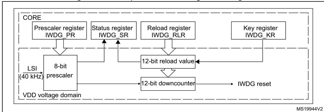
Note: The watchdog function is implemented in the \( V_{DD} \) voltage domain, still functional in Stop and Standby modes.
Table 69. Min/max IWDG timeout period (in ms) at 32 kHz (LSI) (1)
| Prescaler divider | PR[2:0] bits | Min timeout RL[11:0]= 0x000 | Max timeout RL[11:0]= 0xFFF |
|---|---|---|---|
| /4 | 0 | 0.125 | 512 |
| /8 | 1 | 0.25 | 1024 |
| /16 | 2 | 0.5 | 2048 |
| /32 | 3 | 1 | 4096 |
| /64 | 4 | 2 | 8192 |
| /128 | 5 | 4 | 16384 |
| /256 | 6 | 8 | 32768 |
- 1. These timings are given for a 32 kHz clock but the microcontroller internal RC frequency can vary. Refer to the LSI oscillator characteristics table in the device datasheet for maximum and minimum values.
17.4 IWDG registers
Refer to Section 2.2 on page 45 for a list of abbreviations used in register descriptions.
The peripheral registers have to be accessed by half-words (16 bits) or words (32 bits).
17.4.1 Key register (IWDG_KR)
Address offset: 0x00
Reset value: 0x0000 0000 (reset by Standby mode)

| 31 | 30 | 29 | 28 | 27 | 26 | 25 | 24 | 23 | 22 | 21 | 20 | 19 | 18 | 17 | 16 | 15 | 14 | 13 | 12 | 11 | 10 | 9 | 8 | 7 | 6 | 5 | 4 | 3 | 2 | 1 | 0 |
| Reserved | KEY[15:0] | ||||||||||||||||||||||||||||||
| w | w | w | w | w | w | w | w | w | w | w | w | w | w | w | w | ||||||||||||||||
Bits 31:16 Reserved, must be kept at reset value.
Bits 15:0 KEY[15:0] : Key value (write only, read 0000h)
These bits must be written by software at regular intervals with the key value AAAAh, otherwise the watchdog generates a reset when the counter reaches 0.
Writing the key value 5555h to enable access to the IWDG_PR and IWDG_RLR registers (see Section 17.3.2 )
Writing the key value CCCCh starts the watchdog (except if the hardware watchdog option is selected)
17.4.2 Prescaler register (IWDG_PR)
Address offset: 0x04
Reset value: 0x0000 0000

| 31 | 30 | 29 | 28 | 27 | 26 | 25 | 24 | 23 | 22 | 21 | 20 | 19 | 18 | 17 | 16 | 15 | 14 | 13 | 12 | 11 | 10 | 9 | 8 | 7 | 6 | 5 | 4 | 3 | 2 | 1 | 0 |
| Reserved | PR[2:0] | ||||||||||||||||||||||||||||||
| rw | rw | rw | |||||||||||||||||||||||||||||
Bits 31:3 Reserved, must be kept at reset value.
Bits 2:0 PR[2:0] : Prescaler divider
These bits are write access protected see Section 17.3.2 . They are written by software to select the prescaler divider feeding the counter clock. PVU bit of IWDG_SR must be reset in order to be able to change the prescaler divider.
- 000: divider /4
- 001: divider /8
- 010: divider /16
- 011: divider /32
- 100: divider /64
- 101: divider /128
- 110: divider /256
- 111: divider /256
Note: Reading this register returns the prescaler value from the VDD voltage domain. This value may not be up to date/valid if a write operation to this register is ongoing. For this reason the value read from this register is valid only when the PVU bit in the IWDG_SR register is reset.
17.4.3 Reload register (IWDG_RLR)
Address offset: 0x08
Reset value: 0x0000 0FFF (reset by Standby mode)

| 31 | 30 | 29 | 28 | 27 | 26 | 25 | 24 | 23 | 22 | 21 | 20 | 19 | 18 | 17 | 16 | 15 | 14 | 13 | 12 | 11 | 10 | 9 | 8 | 7 | 6 | 5 | 4 | 3 | 2 | 1 | 0 |
| Reserved | RL[11:0] | ||||||||||||||||||||||||||||||
| rw | rw | rw | rw | rw | rw | rw | rw | rw | rw | rw | rw | ||||||||||||||||||||
Bits 31:12 Reserved, must be kept at reset value.
Bits 11:0 RL[11:0] : Watchdog counter reload value
These bits are write access protected see Section 17.3.2 . They are written by software to define the value to be loaded in the watchdog counter each time the value AAAAh is written in the IWDG_KR register. The watchdog counter counts down from this value. The timeout period is a function of this value and the clock prescaler. Refer to Table 69 .
The RVU bit in the IWDG_SR register must be reset in order to be able to change the reload value.
Note: Reading this register returns the reload value from the V DD voltage domain. This value may not be up to date/valid if a write operation to this register is ongoing on this register. For this reason the value read from this register is valid only when the RVU bit in the IWDG_SR register is reset.
17.4.4 Status register (IWDG_SR)
Address offset: 0x0C
Reset value: 0x0000 0000 (not reset by Standby mode)

| 31 | 30 | 29 | 28 | 27 | 26 | 25 | 24 | 23 | 22 | 21 | 20 | 19 | 18 | 17 | 16 | 15 | 14 | 13 | 12 | 11 | 10 | 9 | 8 | 7 | 6 | 5 | 4 | 3 | 2 | 1 | 0 | |
| Reserved | RVU | PVU | ||||||||||||||||||||||||||||||
| r | r | |||||||||||||||||||||||||||||||
Bits 31:2 Reserved, must be kept at reset value.
Bit 1 RVU : Watchdog counter reload value update
This bit is set by hardware to indicate that an update of the reload value is ongoing. It is reset by hardware when the reload value update operation is completed in the V DD voltage domain (takes up to 5 RC 40 kHz cycles).
Reload value can be updated only when RVU bit is reset.
Bit 0 PVU : Watchdog prescaler value update
This bit is set by hardware to indicate that an update of the prescaler value is ongoing. It is reset by hardware when the prescaler update operation is completed in the V DD voltage domain (takes up to 5 RC 40 kHz cycles).
Prescaler value can be updated only when PVU bit is reset.
Note: If several reload values or prescaler values are used by application, it is mandatory to wait until RVU bit is reset before changing the reload value and to wait until PVU bit is reset before changing the prescaler value. However, after updating the prescaler and/or the reload value it is not necessary to wait until RVU or PVU is reset before continuing code execution (even in case of low-power mode entry, the write operation is taken into account and completes)
17.4.5 IWDG register map
The following table gives the IWDG register map and reset values.
Table 70. IWDG register map and reset values
| Offset | Register | 31 | 30 | 29 | 28 | 27 | 26 | 25 | 24 | 23 | 22 | 21 | 20 | 19 | 18 | 17 | 16 | 15 | 14 | 13 | 12 | 11 | 10 | 9 | 8 | 7 | 6 | 5 | 4 | 3 | 2 | 1 | 0 |
|---|---|---|---|---|---|---|---|---|---|---|---|---|---|---|---|---|---|---|---|---|---|---|---|---|---|---|---|---|---|---|---|---|---|
| 0x00 | IWDG_KR | Reserved | KEY[15:0] | ||||||||||||||||||||||||||||||
| Reset value | 0 | 0 | 0 | 0 | 0 | 0 | 0 | 0 | 0 | 0 | 0 | 0 | 0 | 0 | 0 | 0 | |||||||||||||||||
| 0x04 | IWDG_PR | Reserved | PR[2:0] | ||||||||||||||||||||||||||||||
| Reset value | 0 0 0 | ||||||||||||||||||||||||||||||||
| 0x08 | IWDG_RLR | Reserved | RL[11:0] | ||||||||||||||||||||||||||||||
| Reset value | 1 1 1 1 1 1 1 1 1 1 1 1 | ||||||||||||||||||||||||||||||||
| 0x0C | IWDG_SR | Reserved | RVU PVU | ||||||||||||||||||||||||||||||
| Reset value | 0 0 | ||||||||||||||||||||||||||||||||
Refer to Section 3.3: Memory map for the register boundary addresses.