8. Interrupts and events
This Section applies to the whole STM32F20x and STM32F21x family, unless otherwise specified.
8.1 Nested vectored interrupt controller (NVIC)
8.1.1 NVIC features
The nested vector interrupt controller NVIC includes the following features:
- • 81 maskable interrupt channels (not including the 16 interrupt lines of Cortex ® -M3)
- • 16 programmable priority levels (4 bits of interrupt priority are used)
- • low-latency exception and interrupt handling
- • power management control
- • implementation of system control registers
The NVIC and the processor core interface are closely coupled, which enables low latency interrupt processing and efficient processing of late arriving interrupts.
All interrupts including the core exceptions are managed by the NVIC. For more information on exceptions and NVIC programming, refer to PM0056 programming manual.
8.1.2 SysTick calibration value register
The SysTick calibration value is fixed to 15000, which gives a reference time base of 1 ms with the SysTick clock set to 15 MHz (max HCLK/8).
8.1.3 Interrupt and exception vectors
Table 20 is the vector table for the STM32F20x and STM32F21x devices.
Table 20. Vector table
| Position | Priority | Type of priority | Acronym | Description | Address |
|---|---|---|---|---|---|
| - | - | - | Reserved | 0x0000_0000 | |
| -3 | Fixed | Reset | Reset | 0x0000_0004 | |
| -2 | Fixed | NMI | Non maskable interrupt. The RCC Clock Security System (CSS) is linked to the NMI vector. | 0x0000_0008 | |
| -1 | Fixed | HardFault | All class of fault | 0x0000_000C | |
| 0 | Settable | MemManage | Memory management | 0x0000_0010 |
Table 20. Vector table (continued)
| Position | Priority | Type of priority | Acronym | Description | Address |
|---|---|---|---|---|---|
| 1 | Settable | BusFault | Pre-fetch fault, memory access fault | 0x0000_0014 | |
| 2 | Settable | UsageFault | Undefined instruction or illegal state | 0x0000_0018 | |
| - | - | - | Reserved | 0x0000_001C - 0x0000_002B | |
| 3 | Settable | SVCall | System service call via SWI instruction | 0x0000_002C | |
| 4 | Settable | Debug Monitor | Debug Monitor | 0x0000_0030 | |
| - | - | - | Reserved | 0x0000_0034 | |
| 5 | Settable | PendSV | Pendable request for system service | 0x0000_0038 | |
| 6 | Settable | SysTick | System tick timer | 0x0000_003C | |
| 0 | 7 | Settable | WWDG | Window Watchdog interrupt | 0x0000_0040 |
| 1 | 8 | Settable | PVD | PVD through EXTI line detection interrupt | 0x0000_0044 |
| 2 | 9 | Settable | TAMP_STAMP | Tamper and TimeStamp interrupts through the EXTI line | 0x0000_0048 |
| 3 | 10 | Settable | RTC_WKUP | RTC wake-up interrupt through the EXTI line | 0x0000_004C |
| 4 | 11 | Settable | FLASH | Flash global interrupt | 0x0000_0050 |
| 5 | 12 | Settable | RCC | RCC global interrupt | 0x0000_0054 |
| 6 | 13 | Settable | EXTI0 | EXTI Line0 interrupt | 0x0000_0058 |
| 7 | 14 | Settable | EXTI1 | EXTI Line1 interrupt | 0x0000_005C |
| 8 | 15 | Settable | EXTI2 | EXTI Line2 interrupt | 0x0000_0060 |
| 9 | 16 | Settable | EXTI3 | EXTI Line3 interrupt | 0x0000_0064 |
| 10 | 17 | Settable | EXTI4 | EXTI Line4 interrupt | 0x0000_0068 |
| 11 | 18 | Settable | DMA1_Stream0 | DMA1 Stream0 global interrupt | 0x0000_006C |
| 12 | 19 | Settable | DMA1_Stream1 | DMA1 Stream1 global interrupt | 0x0000_0070 |
| 13 | 20 | Settable | DMA1_Stream2 | DMA1 Stream2 global interrupt | 0x0000_0074 |
| 14 | 21 | Settable | DMA1_Stream3 | DMA1 Stream3 global interrupt | 0x0000_0078 |
| 15 | 22 | Settable | DMA1_Stream4 | DMA1 Stream4 global interrupt | 0x0000_007C |
| 16 | 23 | Settable | DMA1_Stream5 | DMA1 Stream5 global interrupt | 0x0000_0080 |
| 17 | 24 | Settable | DMA1_Stream6 | DMA1 Stream6 global interrupt | 0x0000_0084 |
Table 20. Vector table (continued)
| Position | Priority | Type of priority | Acronym | Description | Address |
|---|---|---|---|---|---|
| 18 | 25 | Settable | ADC | ADC1, ADC2 and ADC3 global interrupts | 0x0000_0088 |
| 19 | 26 | Settable | CAN1_TX | CAN1 TX interrupts | 0x0000_008C |
| 20 | 27 | Settable | CAN1_RX0 | CAN1 RX0 interrupts | 0x0000_0090 |
| 21 | 28 | Settable | CAN1_RX1 | CAN1 RX1 interrupt | 0x0000_0094 |
| 22 | 29 | Settable | CAN1_SCE | CAN1 SCE interrupt | 0x0000_0098 |
| 23 | 30 | Settable | EXTI9_5 | EXTI Line[9:5] interrupts | 0x0000_009C |
| 24 | 31 | Settable | TIM1_BRK_TIM9 | TIM1 Break interrupt and TIM9 global interrupt | 0x0000_00A0 |
| 25 | 32 | Settable | TIM1_UP_TIM10 | TIM1 Update interrupt and TIM10 global interrupt | 0x0000_00A4 |
| 26 | 33 | Settable | TIM1_TRG_COM_TIM11 | TIM1 Trigger and Commutation interrupts and TIM11 global interrupt | 0x0000_00A8 |
| 27 | 34 | Settable | TIM1_CC | TIM1 Capture Compare interrupt | 0x0000_00AC |
| 28 | 35 | Settable | TIM2 | TIM2 global interrupt | 0x0000_00B0 |
| 29 | 36 | Settable | TIM3 | TIM3 global interrupt | 0x0000_00B4 |
| 30 | 37 | Settable | TIM4 | TIM4 global interrupt | 0x0000_00B8 |
| 31 | 38 | Settable | I2C1_EV | I 2 C1 event interrupt | 0x0000_00BC |
| 32 | 39 | Settable | I2C1_ER | I 2 C1 error interrupt | 0x0000_00C0 |
| 33 | 40 | Settable | I2C2_EV | I 2 C2 event interrupt | 0x0000_00C4 |
| 34 | 41 | Settable | I2C2_ER | I 2 C2 error interrupt | 0x0000_00C8 |
| 35 | 42 | Settable | SPI1 | SPI1 global interrupt | 0x0000_00CC |
| 36 | 43 | Settable | SPI2 | SPI2 global interrupt | 0x0000_00D0 |
| 37 | 44 | Settable | USART1 | USART1 global interrupt | 0x0000_00D4 |
| 38 | 45 | Settable | USART2 | USART2 global interrupt | 0x0000_00D8 |
| 39 | 46 | Settable | USART3 | USART3 global interrupt | 0x0000_00DC |
| 40 | 47 | Settable | EXTI15_10 | EXTI Line[15:10] interrupts | 0x0000_00E0 |
| 41 | 48 | Settable | RTC_Alarm | RTC Alarms (A and B) through EXTI line interrupt | 0x0000_00E4 |
| 42 | 49 | Settable | OTG_FS_WKUP | USB On-The-Go FS wake-up through EXTI line interrupt | 0x0000_00E8 |
| 43 | 50 | Settable | TIM8_BRK_TIM12 | TIM8 Break interrupt and TIM12 global interrupt | 0x0000_00EC |
Table 20. Vector table (continued)
| Position | Priority | Type of priority | Acronym | Description | Address |
|---|---|---|---|---|---|
| 44 | 51 | Settable | TIM8_UP_TIM13 | TIM8 Update interrupt and TIM13 global interrupt | 0x0000_00F0 |
| 45 | 52 | Settable | TIM8_TRG_COM_TIM14 | TIM8 Trigger and Commutation interrupts and TIM14 global interrupt | 0x0000_00F4 |
| 46 | 53 | Settable | TIM8_CC | TIM8 Capture Compare interrupt | 0x0000_00F8 |
| 47 | 54 | Settable | DMA1_Stream7 | DMA1 Stream7 global interrupt | 0x0000_00FC |
| 48 | 55 | Settable | FSMC | FSMC global interrupt | 0x0000_0100 |
| 49 | 56 | Settable | SDIO | SDIO global interrupt | 0x0000_0104 |
| 50 | 57 | Settable | TIM5 | TIM5 global interrupt | 0x0000_0108 |
| 51 | 58 | Settable | SPI3 | SPI3 global interrupt | 0x0000_010C |
| 52 | 59 | Settable | UART4 | UART4 global interrupt | 0x0000_0110 |
| 53 | 60 | Settable | UART5 | UART5 global interrupt | 0x0000_0114 |
| 54 | 61 | Settable | TIM6_DAC | TIM6 global interrupt, DAC1 and DAC2 underrun error interrupts | 0x0000_0118 |
| 55 | 62 | Settable | TIM7 | TIM7 global interrupt | 0x0000_011C |
| 56 | 63 | Settable | DMA2_Stream0 | DMA2 Stream0 global interrupt | 0x0000_0120 |
| 57 | 64 | Settable | DMA2_Stream1 | DMA2 Stream1 global interrupt | 0x0000_0124 |
| 58 | 65 | Settable | DMA2_Stream2 | DMA2 Stream2 global interrupt | 0x0000_0128 |
| 59 | 66 | Settable | DMA2_Stream3 | DMA2 Stream3 global interrupt | 0x0000_012C |
| 60 | 67 | Settable | DMA2_Stream4 | DMA2 Stream4 global interrupt | 0x0000_0130 |
| 61 | 68 | Settable | ETH | Ethernet global interrupt | 0x0000_0134 |
| 62 | 69 | Settable | ETH_WKUP | Ethernet wake-up through EXTI line interrupt | 0x0000_0138 |
| 63 | 70 | Settable | CAN2_TX | CAN2 TX interrupts | 0x0000_013C |
| 64 | 71 | Settable | CAN2_RX0 | CAN2 RX0 interrupts | 0x0000_0140 |
| 65 | 72 | Settable | CAN2_RX1 | CAN2 RX1 interrupt | 0x0000_0144 |
| 66 | 73 | Settable | CAN2_SCE | CAN2 SCE interrupt | 0x0000_0148 |
| 67 | 74 | Settable | OTG_FS | USB On The Go FS global interrupt | 0x0000_014C |
| 68 | 75 | Settable | DMA2_Stream5 | DMA2 Stream5 global interrupt | 0x0000_0150 |
| 69 | 76 | Settable | DMA2_Stream6 | DMA2 Stream6 global interrupt | 0x0000_0154 |
| 70 | 77 | Settable | DMA2_Stream7 | DMA2 Stream7 global interrupt | 0x0000_0158 |
Table 20. Vector table (continued)
| Position | Priority | Type of priority | Acronym | Description | Address |
|---|---|---|---|---|---|
| 71 | 78 | Settable | USART6 | USART6 global interrupt | 0x0000_015C |
| 72 | 79 | Settable | I2C3_EV | I 2 C3 event interrupt | 0x0000_0160 |
| 73 | 80 | Settable | I2C3_ER | I 2 C3 error interrupt | 0x0000_0164 |
| 74 | 81 | Settable | OTG_HS_EP1_OUT | USB On The Go HS End Point 1 Out global interrupt | 0x0000_0168 |
| 75 | 82 | Settable | OTG_HS_EP1_IN | USB On The Go HS End Point 1 In global interrupt | 0x0000_016C |
| 76 | 83 | Settable | OTG_HS_WKUP | USB On The Go HS wake-up through EXTI interrupt | 0x0000_0170 |
| 77 | 84 | Settable | OTG_HS | USB On The Go HS global interrupt | 0x0000_0174 |
| 78 | 85 | Settable | DCMI | DCMI global interrupt | 0x0000_0178 |
| 79 | 86 | Settable | CRYP | CRYP crypto global interrupt | 0x0000_017C |
| 80 | 87 | Settable | HASH_RNG | Hash and Rng global interrupt | 0x0000_0180 |
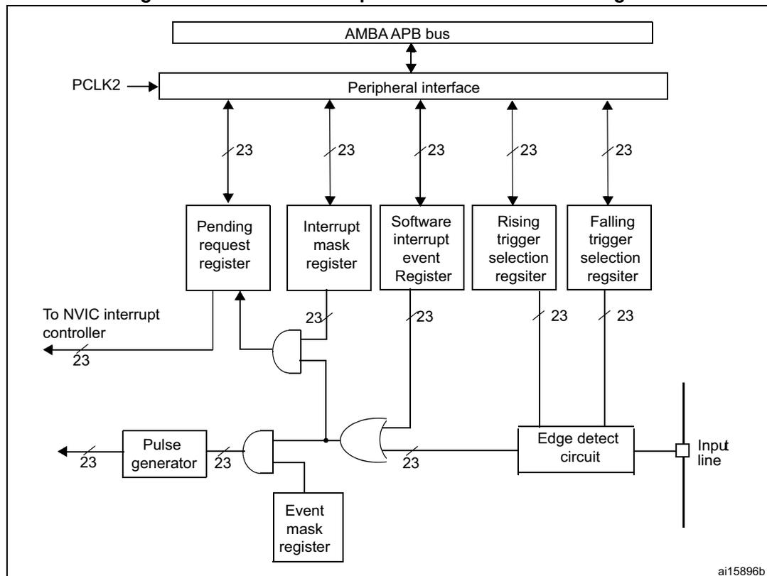
8.2 External interrupt/event controller (EXTI)
The external interrupt/event controller consists of up to 23 edge detectors for generating event/interrupt requests. Each input line can be independently configured to select the type (interrupt or event) and the corresponding trigger event (rising or falling or both). Each line can also be masked independently. A pending register maintains the status line of the interrupt requests.
8.2.1 EXTI main features
The main features of the EXTI controller are the following:
- • independent trigger and mask on each interrupt/event line
- • dedicated status bit for each interrupt line
- • generation of up to 23 software event/interrupt requests
- • detection of external signals with a pulse width lower than the APB2 clock period. Refer to the electrical characteristics section of the STM32F20x and STM32F21x datasheets for details on this parameter.
8.2.2 EXTI block diagram
Figure 19 shows the block diagram.
Figure 19. External interrupt/event controller block diagram
8.2.3 Wake-up event management
The STM32F20x and STM32F21x are able to handle external or internal events in order to wake up the core (WFE). The wake-up event can be generated either by:
- • enabling an interrupt in the peripheral control register but not in the NVIC, and enabling the SEVONPEND bit in the Cortex®-M3 System Control register. When the MCU resumes from WFE, the peripheral interrupt pending bit and the peripheral NVIC IRQ channel pending bit (in the NVIC interrupt clear pending register) have to be cleared.
- • or configuring an external or internal EXTI line in event mode. When the CPU resumes from WFE, it is not necessary to clear the peripheral interrupt pending bit or the NVIC IRQ channel pending bit as the pending bit corresponding to the event line is not set.
To use an external line as a wake-up event, refer to Section 8.2.4: Functional description .
8.2.4 Functional description
To generate the interrupt, the interrupt line should be configured and enabled. This is done by programming the two trigger registers with the desired edge detection and by enabling the interrupt request by writing a '1' to the corresponding bit in the interrupt mask register. When the selected edge occurs on the external interrupt line, an interrupt request is
generated. The pending bit corresponding to the interrupt line is also set. This request is reset by writing a '1' in the pending register.
To generate the event, the event line should be configured and enabled. This is done by programming the two trigger registers with the desired edge detection and by enabling the event request by writing a '1' to the corresponding bit in the event mask register. When the selected edge occurs on the event line, an event pulse is generated. The pending bit corresponding to the event line is not set.
An interrupt/event request can also be generated by software by writing a '1' in the software interrupt/event register.
Hardware interrupt selection
To configure the 23 lines as interrupt sources, use the following procedure:
- • Configure the mask bits of the 23 interrupt lines (EXTI_IMR)
- • Configure the Trigger selection bits of the interrupt lines (EXTI_RTSR and EXTI_FTSR)
- • Configure the enable and mask bits that control the NVIC IRQ channel mapped to the external interrupt controller (EXTI) so that an interrupt coming from one of the 23 lines can be correctly acknowledged.
Hardware event selection
To configure the 23 lines as event sources, use the following procedure:
- • Configure the mask bits of the 23 event lines (EXTI_EMR)
- • Configure the Trigger selection bits of the event lines (EXTI_RTSR and EXTI_FTSR)
Software interrupt/event selection
The 23 lines can be configured as software interrupt/event lines. The following is the procedure to generate a software interrupt.
- • Configure the mask bits of the 23 interrupt/event lines (EXTI_IMR, EXTI_EMR)
- • Set the required bit in the software interrupt register (EXTI_SWIER)
8.2.5 External interrupt/event line mapping
The 140 GPIOs are connected to the 16 external interrupt/event lines in the following manner:
Figure 20. External interrupt/event GPIO mapping
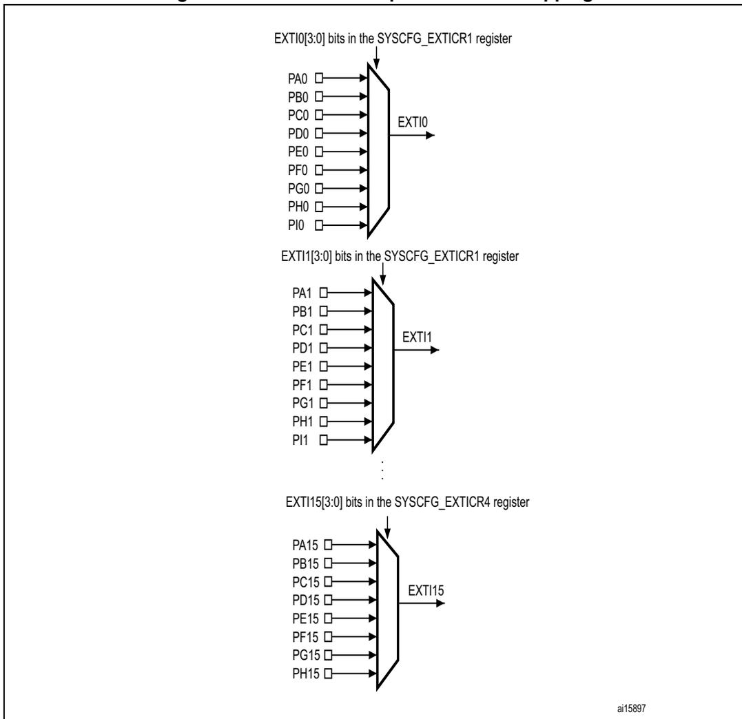
The diagram illustrates the mapping of GPIOs to external interrupt lines. It is divided into three main sections, each representing a different interrupt line and its associated GPIOs.
- EXTI0: This section shows a multiplexer with 10 inputs labeled PA0, PB0, PC0, PD0, PE0, PF0, PG0, PH0, and PI0. Above the multiplexer, the text "EXTI0[3:0] bits in the SYSCFG_EXTICR1 register" indicates the control bits. The output of the multiplexer is labeled EXTI0.
- EXTI1: This section shows a similar multiplexer with 10 inputs labeled PA1, PB1, PC1, PD1, PE1, PF1, PG1, PH1, and PI1. Above it, the text "EXTI1[3:0] bits in the SYSCFG_EXTICR1 register" indicates the control bits. The output is labeled EXTI1.
- EXTI15: This section shows a multiplexer with 8 inputs labeled PA15, PB15, PC15, PD15, PE15, PF15, PG15, and PH15. Above it, the text "EXTI15[3:0] bits in the SYSCFG_EXTICR4 register" indicates the control bits. The output is labeled EXTI15.
There is a vertical ellipsis between the EXTI1 and EXTI15 sections, indicating that the same pattern repeats for the remaining interrupt lines. A small code "ai15897" is visible in the bottom right corner of the diagram area.
The seven other EXTI lines are connected as follows:
- • EXTI line 16 is connected to the PVD output
- • EXTI line 17 is connected to the RTC Alarm event
- • EXTI line 18 is connected to the USB OTG FS Wake-up event
- • EXTI line 19 is connected to the Ethernet Wake-up event
- • EXTI line 20 is connected to the USB OTG HS (configured in FS) Wake-up event
- • EXTI line 21 is connected to the RTC Tamper and TimeStamp events
- • EXTI line 22 is connected to the RTC Wake-up event
8.3 EXTI registers
Refer to Section 1.2 on page 46 for a list of abbreviations used in register descriptions.
The peripheral registers have to be accessed by words (32 bits).
8.3.1 Interrupt mask register (EXTI_IMR)
Address offset: 0x00
Reset value: 0x0000 0000
| 31 | 30 | 29 | 28 | 27 | 26 | 25 | 24 | 23 | 22 | 21 | 20 | 19 | 18 | 17 | 16 |
|---|---|---|---|---|---|---|---|---|---|---|---|---|---|---|---|
| Reserved | MR22 | MR21 | MR20 | MR19 | MR18 | MR17 | MR16 | ||||||||
| r/w | r/w | r/w | r/w | r/w | r/w | r/w | |||||||||
| 15 | 14 | 13 | 12 | 11 | 10 | 9 | 8 | 7 | 6 | 5 | 4 | 3 | 2 | 1 | 0 |
| MR15 | MR14 | MR13 | MR12 | MR11 | MR10 | MR9 | MR8 | MR7 | MR6 | MR5 | MR4 | MR3 | MR2 | MR1 | MR0 |
| r/w | r/w | r/w | r/w | r/w | r/w | r/w | r/w | r/w | r/w | r/w | r/w | r/w | r/w | r/w | r/w |
Bits 31:23 Reserved, must be kept at reset value (0).
Bits 22:0 MRx : Interrupt mask on line x
0: Interrupt request from line x is masked
1: Interrupt request from line x is not masked
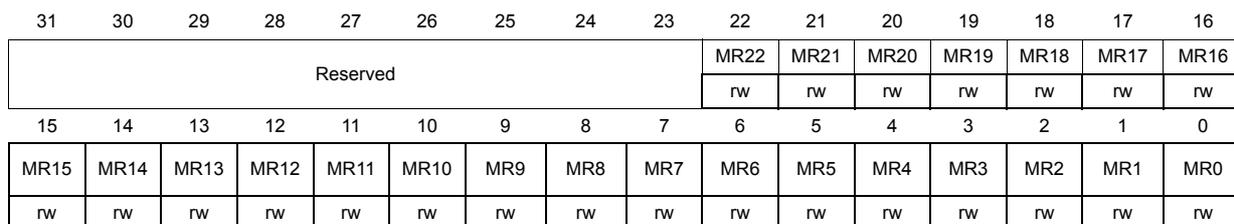
8.3.2 Event mask register (EXTI_EMR)
Address offset: 0x04
Reset value: 0x0000 0000

| 31 | 30 | 29 | 28 | 27 | 26 | 25 | 24 | 23 | 22 | 21 | 20 | 19 | 18 | 17 | 16 |
|---|---|---|---|---|---|---|---|---|---|---|---|---|---|---|---|
| Reserved | MR22 | MR21 | MR20 | MR19 | MR18 | MR17 | MR16 | ||||||||
| r/w | r/w | r/w | r/w | r/w | r/w | r/w | |||||||||
| 15 | 14 | 13 | 12 | 11 | 10 | 9 | 8 | 7 | 6 | 5 | 4 | 3 | 2 | 1 | 0 |
| MR15 | MR14 | MR13 | MR12 | MR11 | MR10 | MR9 | MR8 | MR7 | MR6 | MR5 | MR4 | MR3 | MR2 | MR1 | MR0 |
| r/w | r/w | r/w | r/w | r/w | r/w | r/w | r/w | r/w | r/w | r/w | r/w | r/w | r/w | r/w | r/w |
Bits 31:23 Reserved, must be kept at reset value (0).
Bits 22:0 MRx : Event mask on line x
0: Event request from line x is masked
1: Event request from line x is not masked
8.3.3 Rising trigger selection register (EXTI_RTSR)
Address offset: 0x08
Reset value: 0x0000 0000
| 31 | 30 | 29 | 28 | 27 | 26 | 25 | 24 | 23 | 22 | 21 | 20 | 19 | 18 | 17 | 16 |
|---|---|---|---|---|---|---|---|---|---|---|---|---|---|---|---|
| Reserved | TR22 | TR21 | TR20 | TR19 | TR18 | TR17 | TR16 | ||||||||
| rw | rw | rw | rw | rw | rw | rw | |||||||||
| 15 | 14 | 13 | 12 | 11 | 10 | 9 | 8 | 7 | 6 | 5 | 4 | 3 | 2 | 1 | 0 |
| TR15 | TR14 | TR13 | TR12 | TR11 | TR10 | TR9 | TR8 | TR7 | TR6 | TR5 | TR4 | TR3 | TR2 | TR1 | TR0 |
| rw | rw | rw | rw | rw | rw | rw | rw | rw | rw | rw | rw | rw | rw | rw | rw |
Bits 31:23 Reserved, must be kept at reset value (0).
Bits 22:0 TRx : Rising trigger event configuration bit of line x
0: Rising trigger disabled (for Event and Interrupt) for input line
1: Rising trigger enabled (for Event and Interrupt) for input line
Note: The external wake-up lines are edge triggered, no glitch must be generated on these lines. If a rising edge occurs on the external interrupt line while writing to the EXTI_RTSR register, the pending bit is set.
Rising and falling edge triggers can be set for the same interrupt line. In this configuration, both generate a trigger condition.
8.3.4 Falling trigger selection register (EXTI_FTSR)
Address offset: 0x0C
Reset value: 0x0000 0000
| 31 | 30 | 29 | 28 | 27 | 26 | 25 | 24 | 23 | 22 | 21 | 20 | 19 | 18 | 17 | 16 |
|---|---|---|---|---|---|---|---|---|---|---|---|---|---|---|---|
| Reserved | TR22 | TR21 | TR20 | TR19 | TR18 | TR17 | TR16 | ||||||||
| rw | rw | rw | rw | rw | rw | rw | |||||||||
| 15 | 14 | 13 | 12 | 11 | 10 | 9 | 8 | 7 | 6 | 5 | 4 | 3 | 2 | 1 | 0 |
| TR15 | TR14 | TR13 | TR12 | TR11 | TR10 | TR9 | TR8 | TR7 | TR6 | TR5 | TR4 | TR3 | TR2 | TR1 | TR0 |
| rw | rw | rw | rw | rw | rw | rw | rw | rw | rw | rw | rw | rw | rw | rw | rw |
Bits 31:23 Reserved, must be kept at reset value (0).
Bits 22:0 TRx : Falling trigger event configuration bit of line x
0: Falling trigger disabled (for Event and Interrupt) for input line
1: Falling trigger enabled (for Event and Interrupt) for input line.
Note: The external wake-up lines are edge triggered, no glitch must be generated on these lines. If a falling edge occurs on the external interrupt line while writing to the EXTI_FTSR register, the pending bit is not set.
Rising and falling edge triggers can be set for the same interrupt line. In this configuration, both generate a trigger condition.
8.3.5 Software interrupt event register (EXTI_SWIER)
Address offset: 0x10
Reset value: 0x0000 0000
| 31 | 30 | 29 | 28 | 27 | 26 | 25 | 24 | 23 | 22 | 21 | 20 | 19 | 18 | 17 | 16 |
|---|---|---|---|---|---|---|---|---|---|---|---|---|---|---|---|
| Reserved | SWIER 22 | SWIER 21 | SWIER 20 | SWIER 19 | SWIER 18 | SWIER 17 | SWIER 16 | ||||||||
| rw | rw | rw | rw | rw | rw | rw | |||||||||
| 15 | 14 | 13 | 12 | 11 | 10 | 9 | 8 | 7 | 6 | 5 | 4 | 3 | 2 | 1 | 0 |
| SWIER 15 | SWIER 14 | SWIER 13 | SWIER 12 | SWIER 11 | SWIER 10 | SWIER 9 | SWIER 8 | SWIER 7 | SWIER 6 | SWIER 5 | SWIER 4 | SWIER 3 | SWIER 2 | SWIER 1 | SWIER 0 |
| rw | rw | rw | rw | rw | rw | rw | rw | rw | rw | rw | rw | rw | rw | rw | rw |
Bits 31:23 Reserved, must be kept at reset value (0).
Bits 22:0 SWIERx : Software Interrupt on line x
Writing a 1 to this bit when it is at 0 sets the corresponding pending bit in EXTI_PR. If the interrupt is enabled on this line on the EXTI_IMR and EXTI_EMR, an interrupt request is generated.
This bit is cleared by clearing the corresponding bit in EXTI_PR (by writing a 1 to the bit).
8.3.6 Pending register (EXTI_PR)
Address offset: 0x14
Reset value: undefined
| 31 | 30 | 29 | 28 | 27 | 26 | 25 | 24 | 23 | 22 | 21 | 20 | 19 | 18 | 17 | 16 |
|---|---|---|---|---|---|---|---|---|---|---|---|---|---|---|---|
| Reserved | PR22 | PR21 | PR20 | PR19 | PR18 | PR17 | PR16 | ||||||||
| rc_w1 | rc_w1 | rc_w1 | rc_w1 | rc_w1 | rc_w1 | rc_w1 | |||||||||
| 15 | 14 | 13 | 12 | 11 | 10 | 9 | 8 | 7 | 6 | 5 | 4 | 3 | 2 | 1 | 0 |
| PR15 | PR14 | PR13 | PR12 | PR11 | PR10 | PR9 | PR8 | PR7 | PR6 | PR5 | PR4 | PR3 | PR2 | PR1 | PR0 |
| rc_w1 | rc_w1 | rc_w1 | rc_w1 | rc_w1 | rc_w1 | rc_w1 | rc_w1 | rc_w1 | rc_w1 | rc_w1 | rc_w1 | rc_w1 | rc_w1 | rc_w1 | rc_w1 |
Bits 31:23 Reserved, must be kept at reset value (0).
Bits 22:0 PRx : Pending bit
0: No trigger request occurred
1: selected trigger request occurred
This bit is set when the selected edge event arrives on the external interrupt line. This bit is cleared by writing a 1 to the bit or by changing the sensitivity of the edge detector.
8.3.7 EXTI register map
Table 21 gives the EXTI register map and the reset values.
Table 21. External interrupt/event controller register map and reset values
| Offset | Register | 31 | 30 | 29 | 28 | 27 | 26 | 25 | 24 | 23 | 22 | 21 | 20 | 19 | 18 | 17 | 16 | 15 | 14 | 13 | 12 | 11 | 10 | 9 | 8 | 7 | 6 | 5 | 4 | 3 | 2 | 1 | 0 |
|---|---|---|---|---|---|---|---|---|---|---|---|---|---|---|---|---|---|---|---|---|---|---|---|---|---|---|---|---|---|---|---|---|---|
| 0x00 | EXTI_IMR | Reserved | MR[22:0] | ||||||||||||||||||||||||||||||
| Reset value | 0 | 0 | 0 | 0 | 0 | 0 | 0 | 0 | 0 | 0 | 0 | 0 | 0 | 0 | 0 | 0 | 0 | 0 | 0 | 0 | 0 | 0 | 0 | ||||||||||
| 0x04 | EXTI_EMR | Reserved | MR[22:0] | ||||||||||||||||||||||||||||||
| Reset value | 0 | 0 | 0 | 0 | 0 | 0 | 0 | 0 | 0 | 0 | 0 | 0 | 0 | 0 | 0 | 0 | 0 | 0 | 0 | 0 | 0 | 0 | 0 | ||||||||||
| 0x08 | EXTI_RTSR | Reserved | TR[22:0] | ||||||||||||||||||||||||||||||
| Reset value | 0 | 0 | 0 | 0 | 0 | 0 | 0 | 0 | 0 | 0 | 0 | 0 | 0 | 0 | 0 | 0 | 0 | 0 | 0 | 0 | 0 | 0 | 0 | ||||||||||
| 0x0C | EXTI_FTSR | Reserved | TR[22:0] | ||||||||||||||||||||||||||||||
| Reset value | 0 | 0 | 0 | 0 | 0 | 0 | 0 | 0 | 0 | 0 | 0 | 0 | 0 | 0 | 0 | 0 | 0 | 0 | 0 | 0 | 0 | 0 | 0 | ||||||||||
| 0x10 | EXTI_SWIER | Reserved | SWIER[22:0] | ||||||||||||||||||||||||||||||
| Reset value | 0 | 0 | 0 | 0 | 0 | 0 | 0 | 0 | 0 | 0 | 0 | 0 | 0 | 0 | 0 | 0 | 0 | 0 | 0 | 0 | 0 | 0 | 0 | ||||||||||
| 0x14 | EXTI_PR | Reserved | PR[22:0] | ||||||||||||||||||||||||||||||
| Reset value | 0 | 0 | 0 | 0 | 0 | 0 | 0 | 0 | 0 | 0 | 0 | 0 | 0 | 0 | 0 | 0 | 0 | 0 | 0 | 0 | 0 | 0 | 0 | ||||||||||
Refer to Section 2.3 on page 51 for the register boundary addresses.