5. Reset and clock control (RCC)
5.1 Reset
There are three types of reset, defined as system Reset, power Reset and backup domain Reset.
5.1.1 System reset
A system reset sets all registers to their reset values except the reset flags in the clock controller CSR register and the registers in the Backup domain (see Figure 8 ).
A system reset sets all registers to their reset values unless specified otherwise in the register description
A system reset is generated when one of the following events occurs:
- 1. A low level on the NRST pin (external reset)
- 2. Window watchdog end of count condition (WWDG reset)
- 3. Independent watchdog end of count condition (IWDG reset)
- 4. A software reset (SW reset) (see Software reset )
- 5. Low-power management reset (see Low-power management reset )
Software reset
The reset source can be identified by checking the reset flags in the RCC clock control & status register (RCC_CSR) .
The SYSRESETREQ bit in Cortex ® -M3 Application Interrupt and Reset Control Register must be set to force a software reset on the device. Refer to the Cortex ™ -M3 technical reference manual for more details.
Low-power management reset
There are two ways of generating a low-power management reset:
- 1. Reset generated when entering the Standby mode:
This type of reset is enabled by resetting the nRST_STDBY bit in the user option bytes. In this case, whenever a Standby mode entry sequence is successfully executed, the device is reset instead of entering the Standby mode. - 2. Reset when entering the Stop mode:
This type of reset is enabled by resetting the nRST_STOP bit in the user option bytes. In this case, whenever a Stop mode entry sequence is successfully executed, the device is reset instead of entering the Stop mode.
For further information on the user option bytes, refer to the STM32F20x and STM32F21x Flash programming manual available from your ST sales office.
5.1.2 Power reset
A power reset is generated when one of the following events occurs:
- 1. Power-on/power-down reset (POR/PDR reset) or brownout (BOR) reset
- 2. When exiting the Standby mode
A power reset sets all registers to their reset values except the Backup domain (see Figure 8 )
These sources act on the NRST pin and it is always kept low during the delay phase. The RESET service routine vector is fixed at address 0x0000_0004 in the memory map. For more details, refer to Table 20: Vector table .
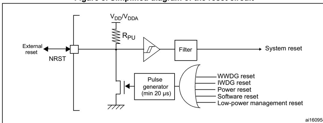
The system reset signal provided to the device is output on the NRST pin. The pulse generator guarantees a minimum reset pulse duration of 20 µs for each internal reset source (external or internal reset). In case of an external reset, the reset pulse is generated while the NRST pin is asserted low.
Figure 8. Simplified diagram of the reset circuit
The Backup domain has two specific resets that affect only the Backup domain (see Figure 8 ).
5.1.3 Backup domain reset
The backup domain reset sets all RTC registers, the RCC_BDCR register and the BRE bit of PWR_CSR register to their reset values. The BKPSRAM is not affected by this reset. The only way of resetting the BKPSRAM is through the Flash interface, by requesting a protection level change from 1 to 0.
Note: Bit DBP of PWR_CR register must be set to 1 to generate the backup domain reset.
A backup domain reset is generated when one of the following events occurs:
- 1. Software reset, triggered by setting the BDRST bit in the RCC Backup domain control register (RCC_BDCR) .
- 2. V DD or V BAT power on, if both supplies have previously been powered off.
5.2 Clocks
Three different clock sources can be used to drive the system clock (SYSCLK):
- • HSI oscillator clock
- • HSE oscillator clock
- • Main PLL (PLL) clock
The devices have the two following secondary clock sources:
- • 32 kHz low-speed internal RC (LSI RC) which drives the independent watchdog and, optionally, the RTC used for Auto-wakeup from the Stop/Standby mode.
- • 32.768 kHz low-speed external crystal (LSE crystal) which optionally drives the RTC clock (RTCCLK)
Each clock source can be switched on or off independently when it is not used, to optimize power consumption.
Figure 9. Clock tree
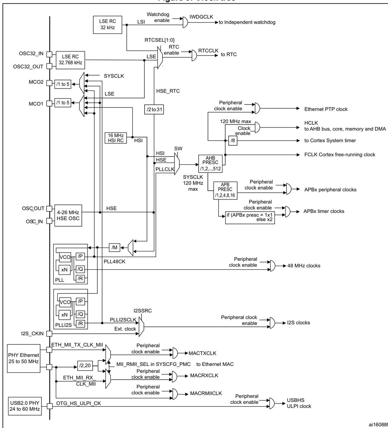
The diagram illustrates the clock tree architecture of an STM32 microcontroller. It shows the following components and connections:
- External Oscillators:
- OSC32_IN / OSC32_OUT: Connected to an LSE RC 32.768 kHz oscillator. This provides the LSI clock to the Watchdog (via IWDGCLK ) and the RTC (via RTCCLK , controlled by RTCSEL[1:0] and RTC enable ).
- OSC_IN / OSC_OUT: Connected to a 4-26 MHz HSE OSC . This provides the HSE clock to the PLL and the SW (System Clock Switch).
- Internal Oscillators:
- 16 MHz HSI RC: Provides the HSI clock to the SW .
- PLL (Phase-Locked Loop):
- Inputs: HSE and HSI .
- Internal components: VCO , xN , /P , /I , /R .
- Outputs: PLL48CK (to 48 MHz clocks via Peripheral clock enable ), PLL12SCLK (to I2S clocks via Peripheral clock enable ), and SYSCLOCK (to SW ).
- SW (System Clock Switch): Selects between HSI , HSE , and PLLCLK to provide the SYSCLOCK (120 MHz max) to the AHB PRESC .
- MCU Output Clocks:
- MCO1 and MCO2 : Can output SYSCLOCK , LSE , or HSE_RTC with a divider of /1 to 5 .
- Peripheral Clock Distribution:
- SYSCLOCK (120 MHz max) is divided by AHB PRESC /1,2,...,512 to provide HCLK (120 MHz max) to the AHB bus, core, memory and DMA .
- HCLK is also divided by /8 to provide the clock to the Cortex System timer .
- SYSCLOCK is divided by APB PRESC /1,2,4,8,16 to provide APBx peripheral clocks and APBx timer clocks (if APBx presc = 1x1 else x2 ).
- Various
Peripheral clock enable
signals control the output of these clocks to specific peripherals:
- Ethernet PTP clock
- MACCTXCLK (to Ethernet MAC)
- MACRXCLK (to Ethernet MAC)
- MACRMIICLK (to Ethernet MAC)
- USBHS ULPI clock (to USB2.0 PHY 24 to 60 MHz)
- Other Connections:
- ETH_MII_TX_CLK_MII (from PHY Ethernet 25 to 50 MHz) is divided by /2,20 to provide MII_RMII_SEL in SYSCFG_PMC to the Ethernet MAC.
- ETH_MII_RX_CLK_MII (from PHY Ethernet 25 to 50 MHz) is used as an input to the Ethernet MAC.
- OTG_HS_ULPI_CK (from USB2.0 PHY 24 to 60 MHz) is used as an input to the USBHS ULPI clock.
- I2S_CKIN is an external clock input to the I2SSRC block, which also selects between PLL12SCLK and Ext. clock to provide I2S clocks .
- 1. For full details about the internal and external clock source characteristics, refer to the Electrical characteristics section in the device datasheet
The clock controller provides a high degree of flexibility to the application in the choice of the external crystal or the oscillator to run the core and peripherals at the highest frequency and, guarantee the appropriate frequency for peripherals that need a specific clock like Ethernet, USB OTG FS and HS, I2S and SDIO.
Several prescalers are used to configure the AHB frequency, the high-speed APB (APB2), and the low-speed APB (APB1) domains. The maximum frequency of the AHB domain is
120 MHz. The maximum allowed frequency of the high-speed APB2 domain is 60 MHz. The maximum allowed frequency of the low-speed APB1 domain is 30 MHz
All peripheral clocks are derived from the system clock (SYSCLK) except for:
- • The USB OTG FS clock (48 MHz), the random analog generator (RNG) clock ( \( \leq 48 \) MHz) and the SDIO clock ( \( \leq 48 \) MHz) which are coming from a specific output of PLL (PLL48CLK)
- • The I2S clock
To achieve high-quality audio performance, the I2S clock can be derived either from a specific PLL (PLLI2S) or from an external clock mapped on the I2S_CKIN pin. For more information about I2S clock frequency and precision, refer to Section 25.4.3: Clock generator . - • The USB OTG HS (60 MHz) clock which is provided from the external PHY
- • The Ethernet MAC clocks (TX, RX and RMII) which are provided from the external PHY. For further information on the Ethernet configuration, refer to Section 28.4.4: MII/RMII selection in the Ethernet peripheral description. When the Ethernet is used, the AHB clock frequency must be at least 25 MHz.
The RCC feeds the external clock of the Cortex System Timer (SysTick) with the AHB clock (HCLK) divided by 8. The SysTick can work either with this clock or with the Cortex clock (HCLK), configurable in the SysTick control and status register.
The timer clock frequencies are automatically set by hardware. There are two cases:
- 1. If the APB prescaler is 1, the timer clock frequencies are set to the same frequency as that of the APB domain to which the timers are connected.
- 2. Otherwise, they are set to twice ( \( \times 2 \) ) the frequency of the APB domain to which the timers are connected.
FCLK acts as Cortex™-M3 free-running clock. For more details, refer to the Cortex™-M3 technical reference manual.
5.2.1 HSE clock
The high speed external clock signal (HSE) can be generated from two possible clock sources:
- • HSE external crystal/ceramic resonator
- • HSE external user clock
The resonator and the load capacitors have to be placed as close as possible to the oscillator pins in order to minimize output distortion and startup stabilization time. The loading capacitance values must be adjusted according to the selected oscillator.
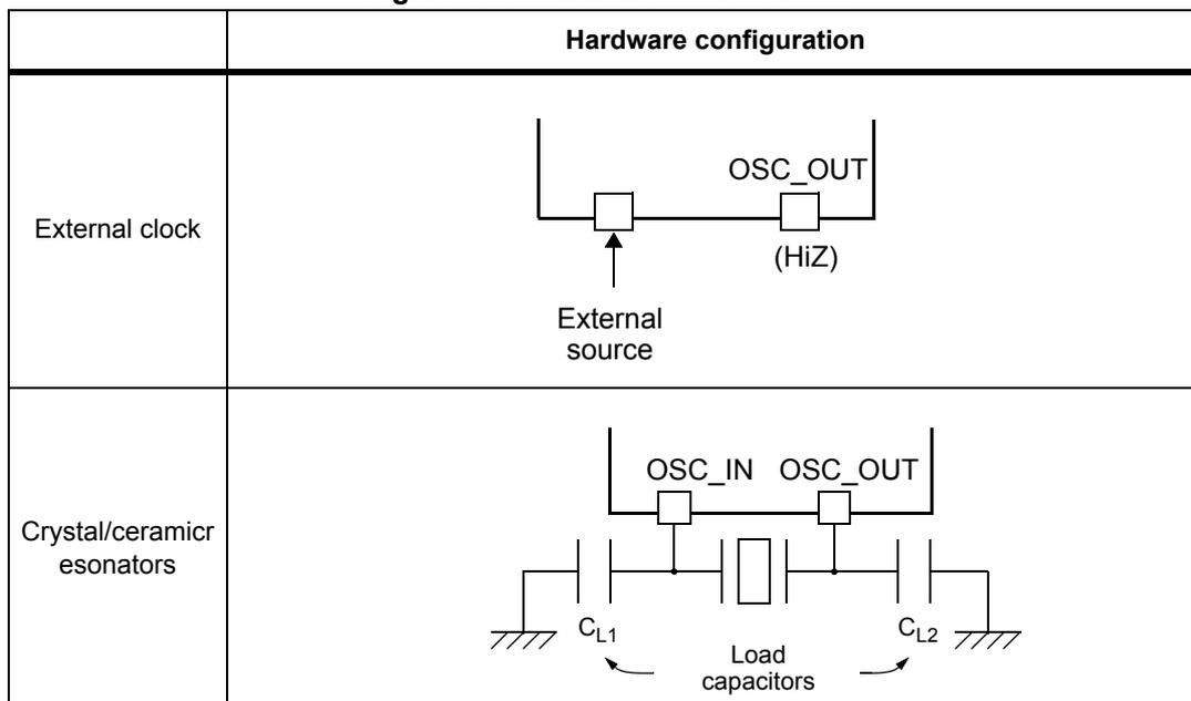
Figure 10. HSE/LSE clock sources
| Hardware configuration | |
|---|---|
| External clock | |
| Crystal/ceramic resonators |
External source (HSE bypass)
In this mode, an external clock source must be provided. You select this mode by setting the HSEBYP and HSEON bits in the RCC clock control register (RCC_CR) . The external clock signal (square, sinus or triangle) with ~50% duty cycle has to drive the OSC_IN pin while the OSC_OUT pin should be left hi-Z. See Figure 10 .
External crystal/ceramic resonator (HSE crystal)
The HSE has the advantage of producing a very accurate rate on the main clock.
The associated hardware configuration is shown in Figure 10 . Refer to the electrical characteristics section of the datasheet for more details.
The HSERDY flag in the RCC clock control register (RCC_CR) indicates if the high-speed external oscillator is stable or not. At startup, the clock is not released until this bit is set by hardware. An interrupt can be generated if enabled in the RCC clock interrupt register (RCC_CIR) .
The HSE Crystal can be switched on and off using the HSEON bit in the RCC clock control register (RCC_CR) .
5.2.2 HSI clock
The HSI clock signal is generated from an internal 16 MHz RC oscillator and can be used directly as a system clock, or used as PLL input.
The HSI RC oscillator has the advantage of providing a clock source at low cost (no external components). It also has a faster startup time than the HSE crystal oscillator however, even with calibration the frequency is less accurate than an external crystal oscillator or ceramic resonator.
Calibration
RC oscillator frequencies can vary from one chip to another due to manufacturing process variations, this is why each device is factory calibrated by ST for 1% accuracy at \( T_A = 25\text{ }^\circ\text{C} \) .
After reset, the factory calibration value is loaded in the HSICAL[7:0] bits in the RCC clock control register (RCC_CR) .
If the application is subject to voltage or temperature variations this may affect the RC oscillator speed. You can trim the HSI frequency in the application using the HSITRIM[4:0] bits in the RCC clock control register (RCC_CR) .
The HSIRDY flag in the RCC clock control register (RCC_CR) indicates if the HSI RC is stable or not. At startup, the HSI RC output clock is not released until this bit is set by hardware.
The HSI RC can be switched on and off using the HSION bit in the RCC clock control register (RCC_CR) .
The HSI signal can also be used as a backup source (auxiliary clock) if the HSE crystal oscillator fails. Refer to Section 5.2.7 .
5.2.3 PLL configuration
The STM32F2xx devices feature two PLLs:
- • A main PLL (PLL) clocked by the HSE or HSI oscillator and featuring two different output clocks:
- – The first output is used to generate the high speed system clock (up to 120 MHz)
- – The second output is used to generate the clock for the USB OTG FS (48 MHz), the random analog generator ( \( \leq 48\text{ MHz} \) ) and the SDIO ( \( \leq 48\text{ MHz} \) ).
- • A dedicated PLL (PLL2S) used to generate an accurate clock to achieve high-quality audio performance on the I2S interface.
Since the main-PLL configuration parameters cannot be changed once PLL is enabled, it is recommended to configure PLL before enabling it (selection of the HSI or HSE oscillator as PLL clock source, and configuration of division factors M, N, P, and Q).
The PLL2S uses the same input clock as PLL (PLLM[5:0] and PLLSRC bits are common to both PLLs). However, the PLL2S has dedicated enable/disable and division factors (N and R) configuration bits. Once the PLL2S is enabled, the configuration parameters cannot be changed.
The two PLLs are disabled by hardware when entering Stop and Standby modes, or when an HSE failure occurs when HSE or PLL (clocked by HSE) are used as system clock. RCC PLL configuration register (RCC_PLLCFGR) and RCC clock configuration register (RCC_CFGR) can be used to configure PLL and PLL2S, respectively.
5.2.4 LSE clock
The LSE crystal is a 32.768 kHz low-speed external (LSE) crystal or ceramic resonator. It has the advantage providing a low-power but highly accurate clock source to the real-time clock peripheral (RTC) for clock/calendar or other timing functions.
The LSE crystal is switched on and off using the LSEON bit in RCC Backup domain control register (RCC_BDCR) .
The LSERDY flag in the RCC Backup domain control register (RCC_BDCR) indicates if the LSE crystal is stable or not. At startup, the LSE crystal output clock signal is not released until this bit is set by hardware. An interrupt can be generated if enabled in the RCC clock interrupt register (RCC_CIR) .
External source (LSE bypass)
In this mode, an external clock source must be provided. It must have a frequency up to 1 MHz. You select this mode by setting the LSEBYP and LSEON bits in the RCC Backup domain control register (RCC_BDCR) . The external clock signal (square, sinus or triangle) with ~50% duty cycle has to drive the OSC32_IN pin while the OSC32_OUT pin should be left Hi-Z. See Figure 10 .
5.2.5 LSI clock
The LSI RC acts as an low-power clock source that can be kept running in Stop and Standby mode for the independent watchdog (IWDG) and Auto-wakeup unit (AWU). The clock frequency is around 32 kHz. For more details, refer to the electrical characteristics section of the datasheets.
The LSI RC can be switched on and off using the LSION bit in the RCC clock control & status register (RCC_CSR) .
The LSIRDY flag in the RCC clock control & status register (RCC_CSR) indicates if the low-speed internal oscillator is stable or not. At startup, the clock is not released until this bit is set by hardware. An interrupt can be generated if enabled in the RCC clock interrupt register (RCC_CIR) .
5.2.6 System clock (SYSCLK) selection
After a system reset, the HSI oscillator is selected as the system clock. When a clock source is used directly or through PLL as the system clock, it is not possible to stop it.
A switch from one clock source to another occurs only if the target clock source is ready (clock stable after startup delay or PLL locked). If a clock source that is not yet ready is selected, the switch occurs when the clock source is ready. Status bits in the RCC clock control register (RCC_CR) indicate which clock(s) is (are) ready and which clock is currently used as the system clock.
5.2.7 Clock security system (CSS)
The clock security system can be activated by software. In this case, the clock detector is enabled after the HSE oscillator startup delay, and disabled when this oscillator is stopped.
If a failure is detected on the HSE clock, this oscillator is automatically disabled, a clock failure event is sent to the break inputs of advanced-control timers TIM1 and TIM8, and an interrupt is generated to inform the software about the failure (clock security system interrupt CSSI), allowing the MCU to perform rescue operations. The CSSI is linked to the Cortex™-M3 NMI (non-maskable interrupt) exception vector.
Note: When the CSS is enabled, if the HSE clock happens to fail, the CSS generates an interrupt, which causes the automatic generation of an NMI. The NMI is executed indefinitely unless the CSS interrupt pending bit is cleared. As a consequence, the application has to clear the CSS interrupt in the NMI ISR by setting the CSSC bit in the Clock interrupt register (RCC_CIR).
If the HSE oscillator is used directly or indirectly as the system clock (indirectly meaning that it is directly used as PLL input clock, and that PLL clock is the system clock) and a failure is detected, then the system clock switches to the HSI oscillator and the HSE oscillator is disabled.
If the HSE oscillator clock was the clock source of PLL used as the system clock when the failure occurred, PLL is also disabled. In this case, if the PLLI2S was enabled, it is also disabled when the HSE fails.
5.2.8 RTC/AWU clock
Once the RTCCLK clock source has been selected, the only possible way of modifying the selection is to reset the power domain.
The RTCCLK clock source can be either the HSE 1 MHz (HSE divided by a programmable prescaler), the LSE or the LSI clock. This is selected by programming the RTCSEL[1:0] bits in the RCC Backup domain control register (RCC_BDCR) and the RTCPRE[4:0] bits in RCC clock configuration register (RCC_CFGR) . This selection cannot be modified without resetting the Backup domain.
If the LSE is selected as the RTC clock, the RTC will work normally if the backup or the system supply disappears. If the LSI is selected as the AWU clock, the AWU state is not guaranteed if the system supply disappears. If the HSE oscillator divided by a value between 2 and 31 is used as the RTC clock, the RTC state is not guaranteed if the backup or the system supply disappears.
The LSE clock is in the Backup domain, whereas the HSE and LSI clocks are not. As a consequence:
- • If LSE is selected as the RTC clock:
- – The RTC continues to work even if the \( V_{DD} \) supply is switched off, provided the \( V_{BAT} \) supply is maintained.
- • If LSI is selected as the Auto-wakeup unit (AWU) clock:
- – The AWU state is not guaranteed if the \( V_{DD} \) supply is powered off. Refer to Section 5.2.5: LSI clock on page 91 for more details on LSI calibration.
- • If the HSE clock is used as the RTC clock:
- – The RTC state is not guaranteed if the \( V_{DD} \) supply is powered off or if the internal voltage regulator is powered off (removing power from the 1.2 V domain).
Note: To read the RTC calendar register when the APB1 clock frequency is less than seven times the RTC clock frequency ( \( f_{APB1} < 7 \times f_{RTCCLK} \) ), the software must read the calendar time and date registers twice. The data are correct if the second read access to RTC_TR gives the same result than the first one. Otherwise a third read access must be performed.
5.2.9 Watchdog clock
If the independent watchdog (IWDG) is started by either hardware option or software access, the LSI oscillator is forced ON and cannot be disabled. After the LSI oscillator temporization, the clock is provided to the IWDG.
5.2.10 Clock-out capability
Two microcontroller clock output (MCO) pins are available:
- • MCO1
You can output four different clock sources onto the MCO1 pin (PA8) using the configurable prescaler (from 1 to 5):
- – HSI clock
- – LSE clock
- – HSE clock
- – PLL clock
The desired clock source is selected using the MCO1PRE[2:0] and MCO1[1:0] bits in the RCC clock configuration register (RCC_CFGR) .
- • MCO2
You can output four different clock sources onto the MCO2 pin (PC9) using the configurable prescaler (from 1 to 5):
- – HSE clock
- – PLL clock
- – System clock (SYSCLK)
- – PLLI2S clock
The desired clock source is selected using the MCO2PRE[2:0] and MCO2 bits in the RCC clock configuration register (RCC_CFGR) .
For the different MCO pins, the corresponding GPIO port has to be programmed in alternate function mode.
The selected clock to output onto MCO must not exceed 100 MHz (the maximum I/O speed).
5.2.11 Internal/external clock measurement using TIM5/TIM11
It is possible to indirectly measure the frequencies of all on-board clock source generators by means of the input capture of TIM5 channel4 and TIM11 channel1 as shown in Figure 11 and Figure 11 .
Internal/external clock measurement using TIM5 channel4
TIM5 has an input multiplexer which allows choosing whether the input capture is triggered by the I/O or by an internal clock. This selection is performed through the TI4_RMP [1:0] bits in the TIM5_OR register.
The primary purpose of having the LSE connected to the channel4 input capture is to be able to precisely measure the HSI (this requires to have the HSI used as the system clock source). The number of HSI clock counts between consecutive edges of the LSE signal provides a measurement of the internal clock period. Taking advantage of the high precision of LSE crystals (typically a few tens of ppm) we can determine the internal clock frequency with the same resolution, and trim the source to compensate for manufacturing-process and/or temperature- and voltage-related frequency deviations.
The HSI oscillator has dedicated, user-accessible calibration bits for this purpose.
The basic concept consists in providing a relative measurement (e.g. HSI/LSE ratio): the precision is therefore tightly linked to the ratio between the two clock sources. The greater the ratio, the better the measurement.
It is also possible to measure the LSI frequency: this is useful for applications that do not have a crystal. The ultralow-power LSI oscillator has a large manufacturing process deviation: by measuring it versus the HSI clock source, it is possible to determine its frequency with the precision of the HSI. The measured value can be used to have more accurate RTC time base timeouts (when LSI is used as the RTC clock source) and/or an IWDG timeout with an acceptable accuracy.
Use the following procedure to measure the LSI frequency:
- 1. Enable the TIM5 timer and configure channel4 in Input capture mode.
- 2. Set the TI4_RMP bits in the TIM5_OR register to 0x01 to connect the LSI clock internally to TIM5 channel4 input capture for calibration purposes.
- 3. Measure the LSI clock frequency using the TIM5 capture/compare 4 event or interrupt.
- 4. Use the measured LSI frequency to update the prescaler of the RTC depending on the desired time base and/or to compute the IWDG timeout.
Figure 11. Frequency measurement with TIM5 in Input capture mode
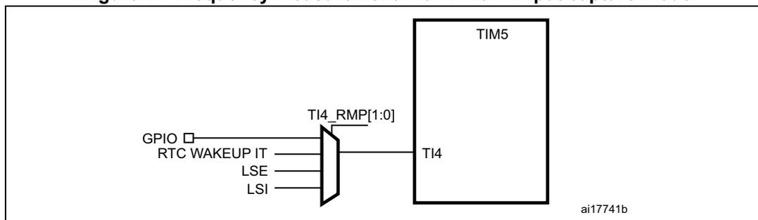
The diagram shows a block labeled 'TIM5'. On its left side, there is an input multiplexer. The multiplexer has four inputs: 'GPIO', 'RTC WAKEUP IT', 'LSE', and 'LSI'. The output of the multiplexer is connected to the 'TI4' input of the 'TIM5' block. Above the multiplexer, the label 'TI4_RMP[1:0]' is present. In the bottom right corner of the diagram, the text 'ai17741b' is visible.
Internal/external clock measurement using TIM11 channel1
TIM11 has an input multiplexer which allows choosing whether the input capture is triggered by the I/O or by an internal clock. This selection is performed through TI1_RMP [1:0] bits in the TIM11_OR register. The HSE_RTC clock (HSE divided by a programmable prescaler) is connected to channel 1 input capture to have a rough indication of the external crystal frequency. This requires that the HSI is the system clock source. This can be useful for instance to ensure compliance with the IEC 60730/IEC 61335 standards which require to be able to determine harmonic or subharmonic frequencies (-50/+100% deviations).
Figure 12. Frequency measurement with TIM11 in Input capture mode
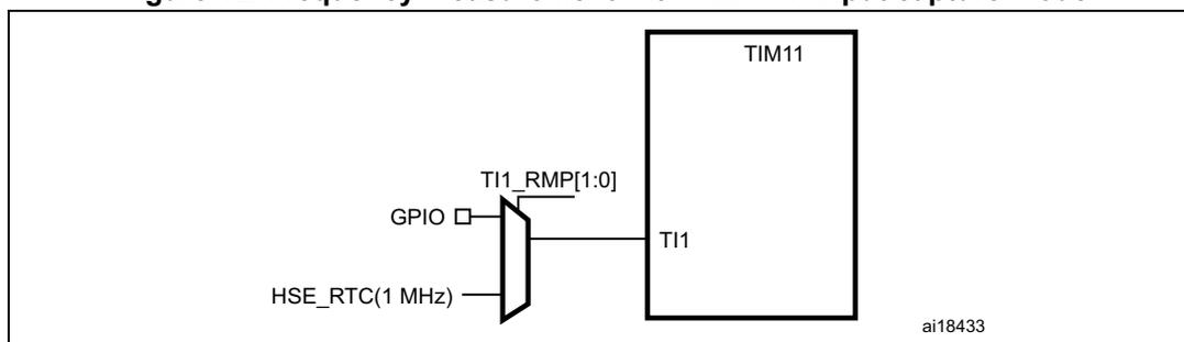
The diagram shows a block labeled 'TIM11'. On its left side, there is an input multiplexer. The multiplexer has two inputs: 'GPIO' and 'HSE_RTC(1 MHz)'. The output of the multiplexer is connected to the 'TI1' input of the 'TIM11' block. Above the multiplexer, the label 'TI1_RMP[1:0]' is present. In the bottom right corner of the diagram, the text 'ai18433' is visible.
5.3 RCC registers
The RCC registers can be accessed by bytes (8 bits), half-words (16 bits) or words (32 bits). Refer to Section 1.2 on page 46 for a list of abbreviations used in register descriptions.
5.3.1 RCC clock control register (RCC_CR)
Address offset: 0x00
Reset value: 0x0000 XX83 where X is undefined.
Access: no wait state, word, half-word and byte access
| 31 | 30 | 29 | 28 | 27 | 26 | 25 | 24 | 23 | 22 | 21 | 20 | 19 | 18 | 17 | 16 |
|---|---|---|---|---|---|---|---|---|---|---|---|---|---|---|---|
| Reserved | PLL2S RDY | PLL2 SON | PLL RDY | PLL
O N | Reserved | CSS ON | HSE BYP | HSE RDY | HSE ON | ||||||
| r | rw | r | rw | rw | rw | r | rw | ||||||||
| 15 | 14 | 13 | 12 | 11 | 10 | 9 | 8 | 7 | 6 | 5 | 4 | 3 | 2 | 1 | 0 |
| HSICAL[7:0] | HSITRIM[4:0] | Res. | HSI RDY | HSIO N | |||||||||||
| r | r | r | r | r | r | r | r | rw | rw | rw | rw | r | rw | ||
Bits 31:28 Reserved, always read as 0.
Bit 27 PLL2SRDY : PLL2S clock ready flag
Set by hardware to indicate that the PLL2S is locked.
0: PLL2S unlocked
1: PLL2S locked
Bit 26 PLL2SON : PLL2S enable
Set and cleared by software to enable PLL2S.
Cleared by hardware when entering Stop or Standby mode.
0: PLL2S OFF
1: PLL2S ON
Bit 25 PLL RDY : Main PLL (PLL) clock ready flag
Set by hardware to indicate that PLL is locked.
0: PLL unlocked
1: PLL locked
Bit 24 PLL ON : Main PLL (PLL) enable
Set and cleared by software to enable PLL.
Cleared by hardware when entering Stop or Standby mode. This bit cannot be reset if PLL clock is used as the system clock.
0: PLL OFF
1: PLL ON
Bits 23:20 Reserved, always read as 0.
Bit 19 CSSON : Clock security system enable
Set and cleared by software to enable the clock security system. When CSSON is set, the clock detector is enabled by hardware when the HSE oscillator is ready, and disabled by hardware if an oscillator failure is detected.
0: Clock security system OFF (Clock detector OFF)
1: Clock security system ON (Clock detector ON if HSE oscillator is stable, OFF if not)
Bit 18 HSEBYP : HSE clock bypass
Set and cleared by software to bypass the oscillator with an external clock. The external clock must be enabled with the HSEON bit, to be used by the device.
The HSEBYP bit can be written only if the HSE oscillator is disabled.
0: HSE oscillator not bypassed
1: HSE oscillator bypassed with an external clock
Bit 17 HSERDY : HSE clock ready flag
Set by hardware to indicate that the HSE oscillator is stable. After the HSEON bit is cleared, HSERDY goes low after 6 HSE oscillator clock cycles.
0: HSE oscillator not ready
1: HSE oscillator ready
Bit 16 HSEON : HSE clock enable
Set and cleared by software.
Cleared by hardware to stop the HSE oscillator when entering Stop or Standby mode. This bit cannot be reset if the HSE oscillator is used directly or indirectly as the system clock.
0: HSE oscillator OFF
1: HSE oscillator ON
Bits 15:8 HSICAL[7:0] : Internal high-speed clock calibration
These bits are initialized automatically at startup.
Bits 7:3 HSITRIM[4:0] : Internal high-speed clock trimming
These bits provide an additional user-programmable trimming value that is added to the HSICAL[7:0] bits. It can be programmed to adjust to variations in voltage and temperature that influence the frequency of the internal HSI RC.
The default value is 16, which, when added to the HSICAL value, should trim the HSI to 16 MHz \( \pm \) 1%. The typical trimming step ( \( F_{\text{HSITRIM}} \) ) between two consecutive HSICAL steps is around 80 kHz.
Bit 2 Reserved, always read as 0.
Bit 1 HSIRDY : Internal high-speed clock ready flag
Set by hardware to indicate that the HSI oscillator is stable. After the HSION bit is cleared, HSIRDY goes low after 6 HSI clock cycles.
0: HSI oscillator not ready
1: HSI oscillator ready
Bit 0 HSION : Internal high-speed clock enable
Set and cleared by software.
Set by hardware to force the HSI oscillator ON when leaving the Stop or Standby mode or in case of a failure of the HSE oscillator used directly or indirectly as the system clock. This bit cannot be cleared if the HSI is used directly or indirectly as the system clock.
0: HSI oscillator OFF
1: HSI oscillator ON
5.3.2 RCC PLL configuration register (RCC_PLLCFGR)
Address offset: 0x04
Reset value: 0x24003010
Access: no wait state, word, half-word and byte access.
This register is used to configure the PLL clock outputs according to the formulas:
- \( f_{\text{(VCO clock)}} = f_{\text{(PLL clock input)}} \times (\text{PLLN} / \text{PLLM}) \)
- • \( f_{(\text{PLL general clock output})} = f_{(\text{VCO clock})} / \text{PLLP} \)
- • \( f_{(\text{USB OTG FS, SDIO, RNG clock output})} = f_{(\text{VCO clock})} / \text{PLLQ} \)
| 31 | 30 | 29 | 28 | 27 | 26 | 25 | 24 | 23 | 22 | 21 | 20 | 19 | 18 | 17 | 16 |
|---|---|---|---|---|---|---|---|---|---|---|---|---|---|---|---|
| Reserved | PLLQ3 | PLLQ2 | PLLQ1 | PLLQ0 | Reserved | PLLSRC | Reserved | PLLP1 | PLLP0 | ||||||
| rw | rw | rw | rw | rw | rw | rw | |||||||||
| 15 | 14 | 13 | 12 | 11 | 10 | 9 | 8 | 7 | 6 | 5 | 4 | 3 | 2 | 1 | 0 |
| Reserved | PLLN8 | PLLN7 | PLLN6 | PLLN5 | PLLN4 | PLLN3 | PLLN2 | PLLN1 | PLLN0 | PLLM5 | PLLM4 | PLLM3 | PLLM2 | PLLM1 | PLLM0 |
| rw | rw | rw | rw | rw | rw | rw | rw | rw | rw | rw | rw | rw | rw | rw | |
Bit 31:28 Reserved, must be kept at reset value.
Bits 27:24 PLLQ : Main PLL (PLL) division factor for USB OTG FS, SDIO and random number generator clocks
Set and cleared by software to control the frequency of USB OTG FS clock, the random number generator clock and the SDIO clock. These bits should be written only if PLL is disabled.
Caution: The USB OTG FS requires a 48 MHz clock to work correctly. The SDIO and the random number generator need a frequency lower than or equal to 48 MHz to work correctly.
USB OTG FS clock frequency = VCO frequency / PLLQ with \( 2 \leq \text{PLLQ} \leq 15 \)
0000: PLLQ = 0, wrong configuration
0001: PLLQ = 1, wrong configuration
0010: PLLQ = 2
0011: PLLQ = 3
0100: PLLQ = 4
...
1111: PLLQ = 15
Bit 23 Reserved, always read as 0.
Bit 22 PLL SRC : Main PLL(PLL) and audio PLL (PLL I2S) entry clock source
Set and cleared by software to select PLL and PLL I2S clock source. This bit can be written only when PLL and PLL I2S are disabled.
0: HSI clock selected as PLL and PLL I2S clock entry
1: HSE oscillator clock selected as PLL and PLL I2S clock entry
Bits 21:18 Reserved, always read as 0.
Bits 17:16 PLLP : Main PLL (PLL) division factor for main system clock
Set and cleared by software to control the frequency of the general PLL output clock. These bits can be written only if PLL is disabled.
Caution: The software has to set these bits correctly not to exceed 120 MHz on this domain.
PLL output clock frequency = VCO frequency / PLLP with PLLP = 2, 4, 6, or 8
00: PLLP = 2
01: PLLP = 4
10: PLLP = 6
11: PLLP = 8
Bits 14:6 PLLN : Main PLL (PLL) multiplication factor for VCO
Set and cleared by software to control the multiplication factor of the VCO. These bits can be written only when PLL is disabled. Only half-word and word accesses are allowed to write these bits.
Caution: The software has to set these bits correctly to ensure that the VCO output frequency is between 192 and 432 MHz.
VCO output frequency = VCO input frequency \( \times \) PLLN with \( 192 \leq PLLN \leq 432 \)
000000000: PLLN = 0, wrong configuration
000000001: PLLN = 1, wrong configuration
...
011000000: PLLN = 192
011000001: PLLN = 193
011000010: PLLN = 194
...
110110000: PLLN = 432
110110001: PLLN = 433, wrong configuration
...
111111111: PLLN = 511, wrong configuration
Bits 5:0 PLLM : Division factor for the main PLL (PLL) and audio PLL (PLLI2S) input clock
Set and cleared by software to divide the PLL and PLLI2S input clock before the VCO. These bits can be written only when the PLL and PLLI2S are disabled.
Caution: The software has to set these bits correctly to ensure that the VCO input frequency ranges from 1 to 2 MHz. It is recommended to select a frequency of 2 MHz to limit PLL jitter.
VCO input frequency = PLL input clock frequency / PLLM with \( 2 \leq PLLM \leq 63 \)
000000: PLLM = 0, wrong configuration
000001: PLLM = 1, wrong configuration
000010: PLLM = 2
000011: PLLM = 3
000100: PLLM = 4
...
111110: PLLM = 62
111111: PLLM = 63
5.3.3 RCC clock configuration register (RCC_CFGR)
Address offset: 0x08
Reset value: 0x0000 0000
Access: \( 0 \leq \text{wait state} \leq 2 \) , word, half-word and byte access
1 or 2 wait states inserted only if the access occurs during a clock source switch.
| 31 | 30 | 29 | 28 | 27 | 26 | 25 | 24 | 23 | 22 | 21 | 20 | 19 | 18 | 17 | 16 |
|---|---|---|---|---|---|---|---|---|---|---|---|---|---|---|---|
| MCO2 | MCO2 PRE[2:0] | MCO1 PRE[2:0] | I2SSC R | MCO1 | RTCPRE[4:0] | ||||||||||
| rw | rw | rw | rw | rw | rw | rw | rw | rw | rw | rw | rw | rw | rw | ||
| 15 | 14 | 13 | 12 | 11 | 10 | 9 | 8 | 7 | 6 | 5 | 4 | 3 | 2 | 1 | 0 |
| PPRE2[2:0] | PPRE1[2:0] | Reserved | HPRE[3:0] | SWS1 | SWS0 | SW1 | SW0 | ||||||||
| rw | rw | rw | rw | rw | rw | rw | rw | rw | rw | r | r | rw | rw | ||
Set and cleared by software. Clock source selection may generate glitches on MCO2. It is highly recommended to configure these bits only after reset before enabling the external oscillators and the PLLs.
00: System clock (SYSCLK) selected
01: PLLI2S clock selected
10: HSE oscillator clock selected
11: PLL clock selected
Bits 27:29 MCO2PRE : MCO2 prescalerSet and cleared by software to configure the prescaler of the MCO2. Modification of this prescaler may generate glitches on MCO2. It is highly recommended to change this prescaler only after reset before enabling the external oscillators and the PLLs.
0xx: no division
100: division by 2
101: division by 3
110: division by 4
111: division by 5
Bits 24:26 MCO1PRE : MCO1 prescalerSet and cleared by software to configure the prescaler of the MCO1. Modification of this prescaler may generate glitches on MCO1. It is highly recommended to change this prescaler only after reset before enabling the external oscillators and the PLL.
0xx: no division
100: division by 2
101: division by 3
110: division by 4
111: division by 5
Bit 23 I2SSRC : I2S clock selectionSet and cleared by software. This bit allows to select the I2S clock source between the PLLI2S clock and the external clock. It is highly recommended to change this bit only after reset and before enabling the I2S module.
0: PLLI2S clock used as I2S clock source
1: External clock mapped on the I2S_CKIN pin used as I2S clock source
Bits 22:21 MCO1 : Microcontroller clock output 1Set and cleared by software. Clock source selection may generate glitches on MCO1. It is highly recommended to configure these bits only after reset before enabling the external oscillators and PLL.
00: HSI clock selected
01: LSE oscillator selected
10: HSE oscillator clock selected
11: PLL clock selected
Bits 20:16 RTCPRE : HSE division factor for RTC clock
Set and cleared by software to divide the HSE clock input clock to generate a 1 MHz clock for RTC.
Caution: The software has to set these bits correctly to ensure that the clock supplied to the RTC is 1 MHz. These bits must be configured if needed before selecting the RTC clock source.
00000: no clock
00001: no clock
00010: HSE/2
00011: HSE/3
00100: HSE/4
...
11110: HSE/30
11111: HSE/31
Bits 15:13 PPRE2 : APB high-speed prescaler (APB2)
Set and cleared by software to control APB high-speed clock division factor.
Caution: The software has to set these bits correctly not to exceed 60 MHz on this domain. The clocks are divided with the new prescaler factor from 1 to 16 AHB cycles after PPRE2 write.
0xx: AHB clock not divided
100: AHB clock divided by 2
101: AHB clock divided by 4
110: AHB clock divided by 8
111: AHB clock divided by 16
Bits 12:10 PPRE1 : APB Low speed prescaler (APB1)
Set and cleared by software to control APB low-speed clock division factor.
Caution: The software has to set these bits correctly not to exceed 30 MHz on this domain. The clocks are divided with the new prescaler factor from 1 to 16 AHB cycles after PPRE1 write.
0xx: AHB clock not divided
100: AHB clock divided by 2
101: AHB clock divided by 4
110: AHB clock divided by 8
111: AHB clock divided by 16
Bits 9:8 Reserved
Bits 7:4 HPRE : AHB prescaler
Set and cleared by software to control AHB clock division factor.
Caution: The clocks are divided with the new prescaler factor from 1 to 16 AHB cycles after HPRE write.
Caution: The AHB clock frequency must be at least 25 MHz when the Ethernet is used.
0xxx: system clock not divided
1000: system clock divided by 2
1001: system clock divided by 4
1010: system clock divided by 8
1011: system clock divided by 16
1100: system clock divided by 64
1101: system clock divided by 128
1110: system clock divided by 256
1111: system clock divided by 512
Bits 3:2 SWS : System clock switch status
Set and cleared by hardware to indicate which clock source is used as the system clock.
00: HSI oscillator used as the system clock
01: HSE oscillator used as the system clock
10: PLL used as the system clock
11: not applicable
Bits 1:0 SW : System clock switch
Set and cleared by software to select the system clock source.
Set by hardware to force the HSI selection when leaving the Stop or Standby mode or in case of failure of the HSE oscillator used directly or indirectly as the system clock.
00: HSI oscillator selected as system clock
01: HSE oscillator selected as system clock
10: PLL selected as system clock
11: not allowed
5.3.4 RCC clock interrupt register (RCC_CIR)
Address offset: 0x0C
Reset value: 0x0000 0000
Access: no wait state, word, half-word and byte access
| 31 | 30 | 29 | 28 | 27 | 26 | 25 | 24 | 23 | 22 | 21 | 20 | 19 | 18 | 17 | 16 |
|---|---|---|---|---|---|---|---|---|---|---|---|---|---|---|---|
| Reserved | CSSC | Reserved | PLL2SRDYC | PLLRDYC | HSE RDYC | HSI RDYC | LSE RDYC | LSI RDYC | |||||||
| w | w | w | w | w | w | w | |||||||||
| 15 | 14 | 13 | 12 | 11 | 10 | 9 | 8 | 7 | 6 | 5 | 4 | 3 | 2 | 1 | 0 |
| Reserved | PLL2SRDYIE | PLLRDYIE | HSE RDYIE | HSI RDYIE | LSE RDYIE | LSI RDYIE | CSSF | Reserved | PLL2SRDYF | PLLRDYF | HSE RDYF | HSI RDYF | LSE RDYF | LSI RDYF | |
| rw | rw | rw | rw | rw | rw | r | r | r | r | r | r | r | |||
Bits 31:24 Reserved, always read as 0.
Bit 23 CSSC : Clock security system interrupt clear
This bit is set by software to clear the CSSF flag.
0: No effect
1: Clear CSSF flag
Bits 22 Reserved, always read as 0.
Bit 21 PLL2SRDYC : PLL2S ready interrupt clear
This bit is set by software to clear the PLL2SRDYF flag.
0: No effect
1: PLL2SRDYF cleared
Bit 20 PLLRDYC : Main PLL(PLL) ready interrupt clear
This bit is set by software to clear the PLLRDYF flag.
0: No effect
1: PLLRDYF cleared
Bit 19 HSERDYC : HSE ready interrupt clear
This bit is set by software to clear the HSERDYF flag.
0: No effect
1: HSERDYF cleared
Bit 18 HSIRDYC : HSI ready interrupt clear
This bit is set software to clear the HSIRDYF flag.
0: No effect
1: HSIRDYF cleared
Bit 17 LSERDYC : LSE ready interrupt clear
This bit is set by software to clear the LSERDYF flag.
0: No effect
1: LSERDYF cleared
Bit 16 LSIRDYC : LSI ready interrupt clear
This bit is set by software to clear the LSIRDYF flag.
0: No effect
1: LSIRDYF cleared
Bits 15:12 Reserved, always read as 0.
Bit 13 PLL2SRDYIE : PLLI2S ready interrupt enable
Set and cleared by software to enable/disable interrupt caused by PLLI2S lock.
0: PLLI2S lock interrupt disabled
1: PLLI2S lock interrupt enabled
Bit 12 PLLRDYIE : Main PLL (PLL) ready interrupt enable
Set and cleared by software to enable/disable interrupt caused by PLL lock.
0: PLL lock interrupt disabled
1: PLL lock interrupt enabled
Bit 11 HSERDYIE : HSE ready interrupt enable
Set and cleared by software to enable/disable interrupt caused by the HSE oscillator stabilization.
0: HSE ready interrupt disabled
1: HSE ready interrupt enabled
Bit 10 HSIRDYIE : HSI ready interrupt enable
Set and cleared by software to enable/disable interrupt caused by the HSI oscillator stabilization.
0: HSI ready interrupt disabled
1: HSI ready interrupt enabled
Bit 9 LSERDYIE : LSE ready interrupt enable
Set and cleared by software to enable/disable interrupt caused by the LSE oscillator stabilization.
0: LSE ready interrupt disabled
1: LSE ready interrupt enabled
Bit 8 LSIRDYIE : LSI ready interrupt enable
Set and cleared by software to enable/disable interrupt caused by LSI oscillator stabilization.
0: LSI ready interrupt disabled
1: LSI ready interrupt enabled
Bit 7 CSSF : Clock security system interrupt flag
Set by hardware when a failure is detected in the HSE oscillator.
Cleared by software setting the CSSC bit.
0: No clock security interrupt caused by HSE clock failure
1: Clock security interrupt caused by HSE clock failure
Bits 6 Reserved, always read as 0.
Bit 5 PLL2SRDYF : PLLI2S ready interrupt flag
Set by hardware when the PLLI2S locks and PLLI2SRDYE is set.
Cleared by software setting the PLLRI2SDYC bit.
0: No clock ready interrupt caused by PLLI2S lock
1: Clock ready interrupt caused by PLLI2S lock
Bit 4 PLLRDYF : Main PLL (PLL) ready interrupt flag
Set by hardware when PLL locks and PLLRDYE is set.
Cleared by software setting the PLLRDYC bit.
0: No clock ready interrupt caused by PLL lock
1: Clock ready interrupt caused by PLL lock
Bit 3 HSERDYF : HSE ready interrupt flag
Set by hardware when External High Speed clock becomes stable and HSERDYE is set.
Cleared by software setting the HSERDYC bit.
0: No clock ready interrupt caused by the HSE oscillator
1: Clock ready interrupt caused by the HSE oscillator
Bit 2 HSIRDYF : HSI ready interrupt flag
Set by hardware when the Internal High Speed clock becomes stable and HSIRDYE is set.
Cleared by software setting the HSIRDYC bit.
0: No clock ready interrupt caused by the HSI oscillator
1: Clock ready interrupt caused by the HSI oscillator
Bit 1 LSERDYF : LSE ready interrupt flag
Set by hardware when the External Low Speed clock becomes stable and LSERDYE is set.
Cleared by software setting the LSERDYC bit.
0: No clock ready interrupt caused by the LSE oscillator
1: Clock ready interrupt caused by the LSE oscillator
Bit 0 LSIRDYF : LSI ready interrupt flag
Set by hardware when the internal low speed clock becomes stable and LSIRDYE is set.
Cleared by software setting the LSIRDYC bit.
0: No clock ready interrupt caused by the LSI oscillator
1: Clock ready interrupt caused by the LSI oscillator
5.3.5 RCC AHB1 peripheral reset register (RCC_AHB1RSTR)
Address offset: 0x10
Reset value: 0x0000 0000
Access: no wait state, word, half-word and byte access.
| 31 | 30 | 29 | 28 | 27 | 26 | 25 | 24 | 23 | 22 | 21 | 20 | 19 | 18 | 17 | 16 |
|---|---|---|---|---|---|---|---|---|---|---|---|---|---|---|---|
| Reserved | OTGHS RST | Reserved | ETHMAC RST | Reserved | DMA2 RST | DMA1 RST | Reserved | ||||||||
| rw | rw | rw | |||||||||||||
| 15 | 14 | 13 | 12 | 11 | 10 | 9 | 8 | 7 | 6 | 5 | 4 | 3 | 2 | 1 | 0 |
| Reserved | CRCRS T | Reserved | GPIOI RST | GPIOH RST | GPIOG RST | GPIOF RST | GPIOE RST | GPIO D RST | GPIOC RST | GPIOB RST | GPIOA RST | ||||
Bits 31:30 Reserved, always read as 0.
Bit 29 OTGHSRST : USB OTG HS module reset
Set and cleared by software.
0: does not reset the USB OTG HS module
1: resets the USB OTG HS module
Bits 28:26 Reserved, always read as 0.
Bit 25 ETHMACRST : Ethernet MAC reset
Set and cleared by software.
0: does not reset Ethernet MAC
1: resets Ethernet MAC
Bits 24:23 Reserved, always read as 0
Bit 22 DMA2RST : DMA2 reset
Set and cleared by software.
0: does not reset DMA2
1: resets DMA2
Bit 21 DMA1RST : DMA2 reset
Set and cleared by software.
0: does not reset DMA2
1: resets DMA2
Bits 20:13 Reserved, always read as 0.
Bit 12 CRCRST : CRC reset
Set and cleared by software.
0: does not reset CRC
1: resets CRC
Bits 11:9 Reserved, always read as 0
Bit 8 GPIOIRST : IO port I reset
Set and cleared by software.
0: does not reset IO port I
1: resets IO port I
Bit 7 GPIOHRST : IO port H reset
Set and cleared by software.
0: does not reset IO port H
1: resets IO port H
Bits 6 GPIOGRST : IO port G reset
Set and cleared by software.
0: does not reset IO port G
1: resets IO port G
- Bit 5
GPIOFRST
: IO port F reset
Set and cleared by software.
0: does not reset IO port F
1: resets IO port F - Bit 4
GPIOERST
: IO port E reset
Set and cleared by software.
0: does not reset IO port E
1: resets IO port E - Bit 3
GPIODRST
: IO port D reset
Set and cleared by software.
0: does not reset IO port D
1: resets IO port D - Bit 2
GPIOCRST
: IO port C reset
Set and cleared by software.
0: does not reset IO port C
1: resets IO port C - Bit 1
GPIOBRST
: IO port B reset
Set and cleared by software.
0: does not reset IO port B
1: resets IO port B - Bit 0
GPIOARST
: IO port A reset
Set and cleared by software.
0: does not reset IO port A
1: resets IO port A
5.3.6 RCC AHB2 peripheral reset register (RCC_AHB2RSTR)
Address offset: 0x14
Reset value: 0x0000 0000
Access: no wait state, word, half-word and byte access
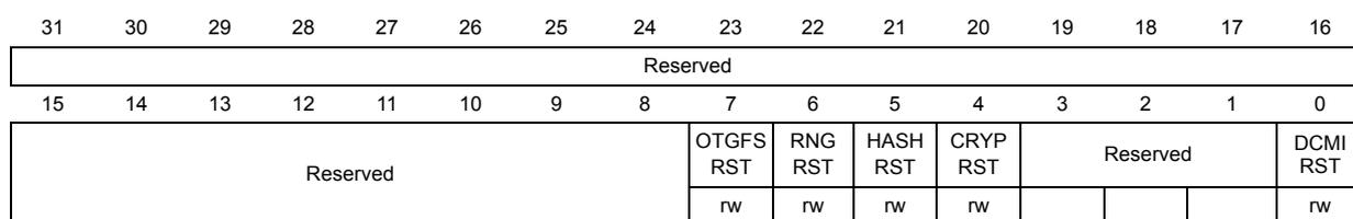
| 31 | 30 | 29 | 28 | 27 | 26 | 25 | 24 | 23 | 22 | 21 | 20 | 19 | 18 | 17 | 16 |
| Reserved | |||||||||||||||
| 15 | 14 | 13 | 12 | 11 | 10 | 9 | 8 | 7 | 6 | 5 | 4 | 3 | 2 | 1 | 0 |
| Reserved | OTGFS RST | RNG RST | HASH RST | CRYP RST | Reserved | DCMI RST | |||||||||
| rw | rw | rw | rw | rw | |||||||||||
Bits 31:8 Reserved, always read as 0.
- Bit 7
OTGFSRST
: USB OTG FS module reset
Set and cleared by software.
0: does not reset the USB OTG FS module
1: resets the USB OTG FS module
- Bit 6
RNGRST
: Random number generator module reset
Set and cleared by software.
0: does not reset the random number generator module
1: resets the random number generator module
- Bit 5
HASHRST
: Hash module reset
Set and cleared by software.
0: does not reset the HASH module
1: resets the HASH module - Bit 4
CRYPRST
: Cryptographic module reset
Set and cleared by software.
0: does not reset the cryptographic module
1: resets the cryptographic module - Bit 3:1 Reserved, always read as 0
- Bit 0
DCMIRST
: Camera interface reset
Set and cleared by software.
0: does not reset the Camera interface
1: resets the Camera interface
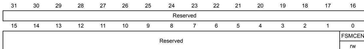
5.3.7 RCC AHB3 peripheral reset register (RCC_AHB3RSTR)
Address offset: 0x18
Reset value: 0x0000 0000
Access: no wait state, word, half-word and byte access.
| 31 | 30 | 29 | 28 | 27 | 26 | 25 | 24 | 23 | 22 | 21 | 20 | 19 | 18 | 17 | 16 |
| Reserved | |||||||||||||||
| 15 | 14 | 13 | 12 | 11 | 10 | 9 | 8 | 7 | 6 | 5 | 4 | 3 | 2 | 1 | 0 |
| Reserved | FSMCRST rw | ||||||||||||||
- Bits 31:1 Reserved, always read as 0.
- Bit 0
FSMCRST
: Flexible static memory controller module reset
Set and cleared by software.
0: does not reset the FSMC module
1: resets the FSMC module
5.3.8 RCC APB1 peripheral reset register (RCC_APB1RSTR)
Address offset: 0x20
Reset value: 0x0000 0000
Access: no wait state, word, half-word and byte access.
| 31 | 30 | 29 | 28 | 27 | 26 | 25 | 24 | 23 | 22 | 21 | 20 | 19 | 18 | 17 | 16 |
|---|---|---|---|---|---|---|---|---|---|---|---|---|---|---|---|
| Reserved | DACRST | PWR RST | Reserved | CAN2 RST | CAN1 RST | Reserved | I2C3 RST | I2C2 RST | I2C1 RST | UART5 RST | UART4 RST | UART3 RST | UART2 RST | Reserved | |
| rw | rw | rw | rw | rw | rw | rw | rw | rw | rw | ||||||
| 15 | 14 | 13 | 12 | 11 | 10 | 9 | 8 | 7 | 6 | 5 | 4 | 3 | 2 | 1 | 0 |
| SPI3 RST | SPI2 RST | Reserved | WWDG RST | Reserved | TIM14 RST | TIM13 RST | TIM12 RST | TIM7 RST | TIM6 RST | TIM5 RST | TIM4 RST | TIM3 RST | |||
| rw | rw | rw | rw | rw | rw | rw | rw | rw | rw | TIM2 RST | |||||
| rw | |||||||||||||||
Bits 31:30 Reserved, always read as 0.
Bit 29 DACRST : DAC reset
Set and cleared by software.
0: does not reset the DAC interface
1: resets the DAC interface
Bit 28 PWRRST : Power interface reset
Set and cleared by software.
0: does not reset the power interface
1: resets the power interface
Bit 27 Reserved, always read as 0
Bit 26 CAN2RST : CAN2 reset
Set and cleared by software.
0: does not reset CAN2
1: resets CAN2
Bit 25 CAN1RST : CAN1 reset
Set and cleared by software.
0: does not reset CAN1
1: resets CAN1
Bit 24 Reserved, always read as 0.
Bit 23 I2C3RST : I2C3 reset
Set and cleared by software.
0: does not reset I2C3
1: resets I2C3
Bit 22 I2C2RST : I2C 2 reset
Set and cleared by software.
0: does not reset I2C2
1: resets I2C 2
Bit 21 I2C1RST : I2C 1 reset
Set and cleared by software.
0: does not reset I2C1
1: resets I2C1
Bit 20 UART5RST : USART 5 reset
Set and cleared by software.
0: does not reset UART5
1: resets UART5
- Bit 19
UART4RST
: USART 4 reset
Set and cleared by software.
0: does not reset UART4
1: resets UART4 - Bit 18
USART3RST
: USART 3 reset
Set and cleared by software.
0: does not reset USART3
1: resets USART3 - Bit 17
USART2RST
: USART 2 reset
Set and cleared by software.
0: does not reset USART2
1: resets USART2 - Bit 16 Reserved, always read as 0.
- Bit 15
SPI3RST
: SPI 3 reset
Set and cleared by software.
0: does not reset SPI3
1: resets SPI3 - Bit 14
SPI2RST
: SPI 2 reset
Set and cleared by software.
0: does not reset SPI2
1: resets SPI2 - Bits 13:12 Reserved, always read as 0.
- Bit 11
WWDGRST
: Window watchdog reset
Set and cleared by software.
0: does not reset the window watchdog
1: resets the window watchdog - Bits 10:9 Reserved, always read as 0.
- Bit 8
TIM14RST
: TIM14 reset
Set and cleared by software.
0: does not reset TIM14
1: resets TIM14 - Bit 7
TIM13RST
: TIM13 reset
Set and cleared by software.
0: does not reset TIM13
1: resets TIM13 - Bit 6
TIM12RST
: TIM12 reset
Set and cleared by software.
0: does not reset TIM12
1: resets TIM12 - Bit 5
TIM7RST
: TIM7 reset
Set and cleared by software.
0: does not reset TIM7
1: resets TIM7
- Bit 4
TIM6RST
: TIM6 reset
Set and cleared by software.
0: does not reset TIM6
1: resets TIM6 - Bit 3
TIM5RST
: TIM5 reset
Set and cleared by software.
0: does not reset TIM5
1: resets TIM5 - Bit 2
TIM4RST
: TIM4 reset
Set and cleared by software.
0: does not reset TIM4
1: resets TIM4 - Bit 1
TIM3RST
: TIM3 reset
Set and cleared by software.
0: does not reset TIM3
1: resets TIM3 - Bit 0
TIM2RST
: TIM2 reset
Set and cleared by software.
0: does not reset TIM2
1: resets TIM2
5.3.9 RCC APB2 peripheral reset register (RCC_APB2RSTR)
Address offset: 0x24
Reset value: 0x0000 0000
Access: no wait state, word, half-word and byte access.
| 31 | 30 | 29 | 28 | 27 | 26 | 25 | 24 | 23 | 22 | 21 | 20 | 19 | 18 | 17 | 16 |
|---|---|---|---|---|---|---|---|---|---|---|---|---|---|---|---|
| Reserved | TIM11 RST | TIM10 RST | TIM9 RST | ||||||||||||
| rw | rw | rw | |||||||||||||
| 15 | 14 | 13 | 12 | 11 | 10 | 9 | 8 | 7 | 6 | 5 | 4 | 3 | 2 | 1 | 0 |
| Reser- ved | SYSCF G RST | Reser- ved | SPI1 RST | SDIO RST | Reserved | ADC RST | Reserved | USART 6 RST | USART 1 RST | Reserved | TIM8 RST | TIM1 RST | |||
| rw | rw | rw | rw | rw | rw | rw | rw | ||||||||
Bits 31:19 Reserved, always read as 0.
- Bit 18
TIM11RST
: TIM11 reset
Set and cleared by software.
0: does not reset TIM11
1: resets TIM14 - Bit 17
TIM10RST
: TIM10 reset
Set and cleared by software.
0: does not reset TIM10
1: resets TIM10
- Bit 16
TIM9RST
: TIM9 reset
Set and cleared by software.
0: does not reset TIM9
1: resets TIM9 - Bit 15 Reserved, always read as 0.
- Bit 14
SYSCFGIRST
: System configuration controller reset
Set and cleared by software.
0: does not reset the System configuration controller
1: resets the System configuration controller - Bit 13 Reserved, always read as 0.
- Bit 12
SPI1RST
: SPI 1 reset
Set and cleared by software.
0: does not reset SPI1
1: resets SPI1 - Bit 11
SDIORST
: SDIO reset
Set and cleared by software.
0: does not reset the SDIO module
1: resets the SDIO module - Bits 10:9 Reserved, always read as 0
- Bit 8
ADCRST
: ADC interface reset (common to all ADCs)
Set and cleared by software.
0: does not reset the ADC interface
1: resets the ADC interface - Bits 7:6 Reserved, always read as 0.
- Bit 5
USART6RST
: USART6 reset
Set and cleared by software.
0: does not reset USART6
1: resets USART6 - Bit 4
USART1RST
: USART1 reset
Set and cleared by software.
0: does not reset USART1
1: resets USART1 - Bits 3:2 Reserved, always read as 0.
- Bit 1
TIM8RST
: TIM8 reset
Set and cleared by software.
0: does not reset TIM8
1: resets TIM8 - Bit 0
TIM1RST
: TIM1 reset
Set and cleared by software.
0: does not reset TIM1
1: resets TIM1
5.3.10 RCC AHB1 peripheral clock register (RCC_AHB1ENR)
Address offset: 0x30
Reset value: 0x0000 0000
Access: no wait state, word, half-word and byte access.
| 31 | 30 | 29 | 28 | 27 | 26 | 25 | 24 | 23 | 22 | 21 | 20 | 19 | 18 | 17 | 16 |
|---|---|---|---|---|---|---|---|---|---|---|---|---|---|---|---|
| Reserved | OTGHS ULPIEN | OTGHS EN | ETHMAC PTPEN | ETHMAC RXEN | ETHMAC TXEN | ETHMAC CEN | Reserved | DMA2EN | DMA1EN | Reserved | BKPSR AMEN | Reserved | |||
| rw | rw | rw | rw | rw | rw | rw | rw | rw | |||||||
| 15 | 14 | 13 | 12 | 11 | 10 | 9 | 8 | 7 | 6 | 5 | 4 | 3 | 2 | 1 | 0 |
|---|---|---|---|---|---|---|---|---|---|---|---|---|---|---|---|
| Reserved | CRCCEN | Reserved | GPIOEN N | GPIOH EN | GPIOE N | GPIOF N | GPIOE EN | GPIO D EN | GPIO C EN | GPIO B EN | GPIO A EN | ||||
| rw | rw | rw | rw | rw | rw | rw | rw | rw | rw | ||||||
Bits 31 Reserved, always read as 0.
Bit 30 OTGHSULPIEN : USB OTG HSULPI clock enable
Set and cleared by software.
0: USB OTG HS ULPI clock disabled
1: USB OTG HS ULPI clock enabled
Bit 29 OTGHSEN : USB OTG HS clock enable
Set and cleared by software.
0: USB OTG HS clock disabled
1: USB OTG HS clock enabled
Bit 28 ETHMACPTPEN : Ethernet PTP clock enable
Set and cleared by software.
0: Ethernet PTP clock disabled
1: Ethernet PTP clock enabled
Bit 27 ETHMACRXEN : Ethernet Reception clock enable
Set and cleared by software.
0: Ethernet Reception clock disabled
1: Ethernet Reception clock enabled
Bit 26 ETHMACTXEN : Ethernet Transmission clock enable
Set and cleared by software.
0: Ethernet Transmission clock disabled
1: Ethernet Transmission clock enabled
Bit 25 ETHMACEN : Ethernet MAC clock enable
Set and cleared by software.
0: Ethernet MAC clock disabled
1: Ethernet MAC clock enabled
Bits 24:23 Reserved, always read as 0.
Bit 22 DMA2EN : DMA2 clock enable
Set and cleared by software.
0: DMA2 clock disabled
1: DMA2 clock enabled
Bit 21 DMA1EN : DMA1 clock enable
Set and cleared by software.
0: DMA1 clock disabled
1: DMA1 clock enabled
Bits 20:19 Reserved, always read as 0.
Bit 18 BKPSRAMEN : Backup SRAM interface clock enable
Set and cleared by software.
0: Backup SRAM interface clock disabled
1: Backup SRAM interface clock enabled
Bits 17:13 Reserved, always read as 0.
Bit 12 CRCEN : CRC clock enable
Set and cleared by software.
0: CRC clock disabled
1: CRC clock enabled
Bits 11:9 Reserved, always read as 0.
Bit 8 GPIOIEN : IO port I clock enable
Set and cleared by software.
0: IO port I clock disabled
1: IO port I clock enabled
Bit 7 GPIOHEN : IO port H clock enable
Set and cleared by software.
0: IO port H clock disabled
1: IO port H clock enabled
Bit 6 GPIOGEN : IO port G clock enable
Set and cleared by software.
0: IO port G clock disabled
1: IO port G clock enabled
Bit 5 GPIOFEN : IO port F clock enable
Set and cleared by software.
0: IO port F clock disabled
1: IO port F clock enabled
Bit 4 GPIOEEN : IO port E clock enable
Set and cleared by software.
0: IO port E clock disabled
1: IO port E clock enabled
Bit 3 GPIO DEN : IO port D clock enable
Set and cleared by software.
0: IO port D clock disabled
1: IO port D clock enabled
Bit 2 GPIOCEN : IO port C clock enable
Set and cleared by software.
0: IO port C clock disabled
1: IO port C clock enabled
Bit 1 GPIOBEN : IO port B clock enable
Set and cleared by software.
0: IO port B clock disabled
1: IO port B clock enabled
Bit 0 GPIOAEN : IO port A clock enable
Set and cleared by software.
0: IO port A clock disabled
1: IO port A clock enabled
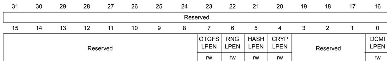
5.3.11 RCC AHB2 peripheral clock enable register (RCC_AHB2ENR)
Address offset: 0x34
Reset value: 0x0000 0000
Access: no wait state, word, half-word and byte access.
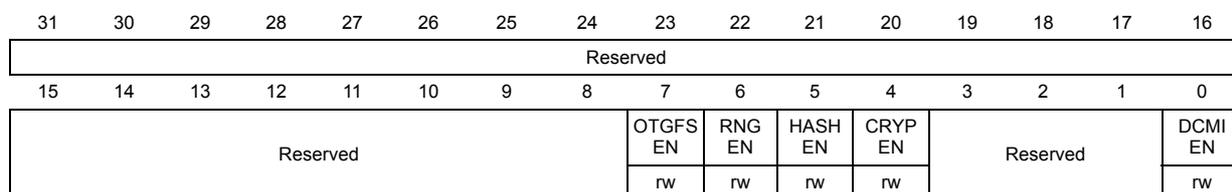
| 31 | 30 | 29 | 28 | 27 | 26 | 25 | 24 | 23 | 22 | 21 | 20 | 19 | 18 | 17 | 16 |
| Reserved | |||||||||||||||
| 15 | 14 | 13 | 12 | 11 | 10 | 9 | 8 | 7 | 6 | 5 | 4 | 3 | 2 | 1 | 0 |
| Reserved | OTGFS EN | RNG EN | HASH EN | CRYP EN | Reserved | DCMI EN | |||||||||
| rw | rw | rw | rw | rw | |||||||||||
Bits 31:8 Reserved, always read as 0.
Bit 7 OTGFSEN : USB OTG FS clock enable
Set and cleared by software.
0: USB OTG FS clock disabled
1: USB OTG FS clock enabled
Bit 6 RNGEN : Random number generator clock enable
Set and cleared by software.
0: Random number generator clock disabled
1: Random number generator clock enabled
Bit 5 HASHEN : Hash modules clock enable
Set and cleared by software.
0: Hash modules clock disabled
1: Hash modules clock enabled
Bit 4 CRYPEN : Cryptographic modules clock enable
Set and cleared by software.
0: cryptographic module clock disabled
1: cryptographic module clock enabled
Bit 3:1 Reserved, always read as 0
Bit 0 DCMIEN : Camera interface enable
Set and cleared by software.
0: Camera interface clock disabled
1: Camera interface clock enabled
5.3.12 RCC AHB3 peripheral clock enable register (RCC_AHB3ENR)
Address offset: 0x38
Reset value: 0x0000 0000
Access: no wait state, word, half-word and byte access.
| 31 | 30 | 29 | 28 | 27 | 26 | 25 | 24 | 23 | 22 | 21 | 20 | 19 | 18 | 17 | 16 |
| Reserved | |||||||||||||||
| 15 | 14 | 13 | 12 | 11 | 10 | 9 | 8 | 7 | 6 | 5 | 4 | 3 | 2 | 1 | 0 |
| Reserved | FSMCEN | ||||||||||||||
| rw | |||||||||||||||
Bits 31:1 Reserved, always read as 0.
Bit 0 FSMCEN : Flexible static memory controller module clock enable
Set and cleared by software.
0: FSMC module clock disabled
1: FSMC module clock enabled
5.3.13 RCC APB1 peripheral clock enable register (RCC_APB1ENR)
Address offset: 0x40
Reset value: 0x0000 0000
Access: no wait state, word, half-word and byte access.
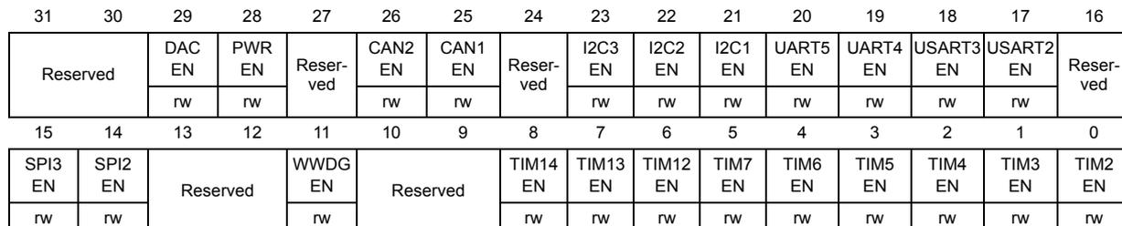
| 31 | 30 | 29 | 28 | 27 | 26 | 25 | 24 | 23 | 22 | 21 | 20 | 19 | 18 | 17 | 16 |
| Reserved | DAC EN | PWR EN | Reserved | CAN2 EN | CAN1 EN | Reserved | I2C3 EN | I2C2 EN | I2C1 EN | UART5 EN | UART4 EN | USART3 EN | USART2 EN | Reserved | |
| rw | rw | rw | rw | rw | rw | rw | rw | rw | rw | ||||||
| 15 | 14 | 13 | 12 | 11 | 10 | 9 | 8 | 7 | 6 | 5 | 4 | 3 | 2 | 1 | 0 |
| SPI3 EN | SPI2 EN | Reserved | WWDG EN | Reserved | TIM14 EN | TIM13 EN | TIM12 EN | TIM7 EN | TIM6 EN | TIM5 EN | TIM4 EN | TIM3 EN | TIM2 EN | ||
| rw | rw | rw | rw | rw | rw | rw | rw | rw | rw | rw | rw | ||||
Bits 31:30 Reserved, always read as 0.
Bit 29 DACEN : DAC interface clock enable
Set and cleared by software.
0: DAC interface clock disabled
1: DAC interface clock enable
Bit 28 PWREN : Power interface clock enable
Set and cleared by software.
0: Power interface clock disabled
1: Power interface clock enable
Bit 27 Reserved, always read as 0.
Bit 26 CAN2EN : CAN 2 clock enable
Set and cleared by software.
0: CAN 2 clock disabled
1: CAN 2 clock enabled
- Bit 25
CAN1EN
: CAN 1 clock enable
Set and cleared by software.
0: CAN 1 clock disabled
1: CAN 1 clock enabled - Bit 24 Reserved, always read as 0.
- Bit 23
I2C3EN
: I2C3 clock enable
Set and cleared by software.
0: I2C3 clock disabled
1: I2C3 clock enabled - Bit 22
I2C2EN
: I2C2 clock enable
Set and cleared by software.
0: I2C2 clock disabled
1: I2C2 clock enabled - Bit 21
I2C1EN
: I2C1 clock enable
Set and cleared by software.
0: I2C1 clock disabled
1: I2C1 clock enabled - Bit 20
UART5EN
: UART5 clock enable
Set and cleared by software.
0: UART5 clock disabled
1: UART5 clock enabled - Bit 19
UART4EN
: UART4 clock enable
Set and cleared by software.
0: UART4 clock disabled
1: UART4 clock enabled - Bit 18
USART3EN
: USART3 clock enable
Set and cleared by software.
0: USART3 clock disabled
1: USART3 clock enabled - Bit 17
USART2EN
: USART 2 clock enable
Set and cleared by software.
0: USART2 clock disabled
1: USART2 clock enabled - Bit 16 Reserved, always read as 0.
- Bit 15
SPI3EN
: SPI3 clock enable
Set and cleared by software.
0: SPI3 clock disabled
1: SPI3 clock enabled - Bit 14
SPI2EN
: SPI2 clock enable
Set and cleared by software.
0: SPI2 clock disabled
1: SPI2 clock enabled - Bits 13:12 Reserved, always read as 0.
- Bit 11
WWDGEN
: Window watchdog clock enable
Set and cleared by software.
0: Window watchdog clock disabled
1: Window watchdog clock enabled - Bit 10:9 Reserved, always read as 0.
- Bit 8
TIM14EN
: TIM14 clock enable
Set and cleared by software.
0: TIM14 clock disabled
1: TIM14 clock enabled - Bit 7
TIM13EN
: TIM13 clock enable
Set and cleared by software.
0: TIM13 clock disabled
1: TIM13 clock enabled - Bit 6
TIM12EN
: TIM12 clock enable
Set and cleared by software.
0: TIM12 clock disabled
1: TIM12 clock enabled - Bit 5
TIM7EN
: TIM7 clock enable
Set and cleared by software.
0: TIM7 clock disabled
1: TIM7 clock enabled - Bit 4
TIM6EN
: TIM6 clock enable
Set and cleared by software.
0: TIM6 clock disabled
1: TIM6 clock enabled - Bit 3
TIM5EN
: TIM5 clock enable
Set and cleared by software.
0: TIM5 clock disabled
1: TIM5 clock enabled - Bit 2
TIM4EN
: TIM4 clock enable
Set and cleared by software.
0: TIM4 clock disabled
1: TIM4 clock enabled - Bit 1
TIM3EN
: TIM3 clock enable
Set and cleared by software.
0: TIM3 clock disabled
1: TIM3 clock enabled - Bit 0
TIM2EN
: TIM2 clock enable
Set and cleared by software.
0: TIM2 clock disabled
1: TIM2 clock enabled
5.3.14 RCC APB2 peripheral clock enable register (RCC_APB2ENR)
Address offset: 0x44
Reset value: 0x0000 0000
Access: no wait state, word, half-word and byte access.
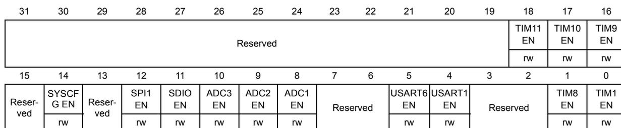
| 31 | 30 | 29 | 28 | 27 | 26 | 25 | 24 | 23 | 22 | 21 | 20 | 19 | 18 | 17 | 16 |
| Reserved | TIM11 EN | TIM10 EN | TIM9 EN | ||||||||||||
| rw | rw | rw | |||||||||||||
| 15 | 14 | 13 | 12 | 11 | 10 | 9 | 8 | 7 | 6 | 5 | 4 | 3 | 2 | 1 | 0 |
| Reser- ved | SYSCF G EN | Reser- ved | SPI1 EN | SDIO EN | ADC3 EN | ADC2 EN | ADC1 EN | Reserved | USART6 EN | USART1 EN | Reserved | TIM8 EN | TIM1 EN | ||
| rw | rw | rw | rw | rw | rw | rw | rw | ||||||||
Bits 31:19 Reserved, always read as 0.
Bit 18 TIM11EN : TIM11 clock enable
Set and cleared by software.
0: TIM11 clock disabled
1: TIM11 clock enabled
Bit 17 TIM10EN : TIM10 clock enable
Set and cleared by software.
0: TIM10 clock disabled
1: TIM10 clock enabled
Bit 16 TIM9EN : TIM9 clock enable
Set and cleared by software.
0: TIM9 clock disabled
1: TIM9 clock enabled
Bit 15 Reserved, always read as 0.
Bit 14 SYSCFGEN : System configuration controller clock enable
Set and cleared by software.
0: System configuration controller clock disabled
1: System configuration controller clock enabled
Bit 13 Reserved, always read as 0.
Bit 12 SPI1EN : SPI1 clock enable
Set and cleared by software.
0: SPI1 clock disabled
1: SPI1 clock enabled
Bit 11 SDIOEN : SDIO clock enable
Set and cleared by software.
0: SDIO module clock disabled
1: SDIO module clock enabled
Bit 10 ADC3EN : ADC3 clock enable
Set and cleared by software.
0: ADC3 clock disabled
1: ADC3 clock disabled
- Bit 9
ADC2EN
: ADC2 clock enable
Set and cleared by software.
0: ADC2 clock disabled
1: ADC2 clock disabled - Bit 8
ADC1EN
: ADC1 clock enable
Set and cleared by software.
0: ADC1 clock disabled
1: ADC1 clock disabled - Bits 7:6 Reserved, always read as 0.
- Bit 5
USART6EN
: USART6 clock enable
Set and cleared by software.
0: USART6 clock disabled
1: USART6 clock enabled - Bit 4
USART1EN
: USART1 clock enable
Set and cleared by software.
0: USART1 clock disabled
1: USART1 clock enabled - Bits 3:2 Reserved, always read as 0.
- Bit 1
TIM8EN
: TIM8 clock enable
Set and cleared by software.
0: TIM8 clock disabled
1: TIM8 clock enabled - Bit 0
TIM1EN
: TIM1 clock enable
Set and cleared by software.
0: TIM1 clock disabled
1: TIM1 clock enabled
5.3.15 RCC AHB1 peripheral clock enable in low power mode register (RCC_AHB1LPENR)
Address offset: 0x50
Reset value: 0x7E67 91FF
Access: no wait state, word, half-word and byte access.
| 31 | 30 | 29 | 28 | 27 | 26 | 25 | 24 | 23 | 22 | 21 | 20 | 19 | 18 | 17 | 16 |
|---|---|---|---|---|---|---|---|---|---|---|---|---|---|---|---|
| Reserved | OTGHS ULPILPEN | OTGHS LPEN | ETHPTP LPEN | ETHRX LPEN | ETH TX LPEN | ETHMAC LPEN | Reserved | DMA2 LPEN | DMA1 LPEN | Reserved | BKPSRAM LPEN | SRAM2 LPEN | |||
| rw | rw | rw | rw | rw | rw | rw | rw | rw | rw | ||||||
| 15 | 14 | 13 | 12 | 11 | 10 | 9 | 8 | 7 | 6 | 5 | 4 | 3 | 2 | 1 | 0 |
| FLITF LPEN | Reserved | CRC LPEN | Reserved | GPIOI LPEN | GPIOH LPEN | GPIOG LPEN | GPIOF LPEN | GPIOE LPEN | GPIO D LPEN | GPIOC LPEN | GPIOB LPEN | GPIOA LPEN | |||
| rw | rw | rw | rw | rw | rw | rw | rw | rw | rw | rw | |||||
- Bit 31 Reserved, always read as 0.
- Bit 30
OTGHSPILPEN
: USB OTG HS ULPI clock enable during Sleep mode
Set and cleared by software.
0: USB OTG HS ULPI clock disabled during Sleep mode
1: USB OTG HS ULPI clock enabled during Sleep mode - Bit 29
OTGHSLPEN
: USB OTG HS clock enable during Sleep mode
Set and cleared by software.
0: USB OTG HS clock disabled during Sleep mode
1: USB OTG HS clock enabled during Sleep mode - Bit 28
ETHMACPTPLPEN
: Ethernet PTP clock enable during Sleep mode
Set and cleared by software.
0: Ethernet PTP clock disabled during Sleep mode
1: Ethernet PTP clock enabled during Sleep mode - Bit 27
ETHMACRXLPEN
: Ethernet reception clock enable during Sleep mode
Set and cleared by software.
0: Ethernet reception clock disabled during Sleep mode
1: Ethernet reception clock enabled during Sleep mode - Bit 26
ETHMACTXLPEN
: Ethernet transmission clock enable during Sleep mode
Set and cleared by software.
0: Ethernet transmission clock disabled during sleep mode
1: Ethernet transmission clock enabled during sleep mode - Bit 25
ETHMACLPEN
: Ethernet MAC clock enable during Sleep mode
Set and cleared by software.
0: Ethernet MAC clock disabled during Sleep mode
1: Ethernet MAC clock enabled during Sleep mode - Bits 24:23 Reserved, always read as 0
- Bit 22
DMA2LPEN
: DMA2 clock enable during Sleep mode
Set and cleared by software.
0: DMA2 clock disabled during Sleep mode
1: DMA2 clock enabled during Sleep mode - Bit 21
DMA1LPEN
: DMA1 clock enable during Sleep mode
Set and cleared by software.
0: DMA1 clock disabled during Sleep mode
1: DMA1 clock enabled during Sleep mode - Bits 20:19 Reserved, always read as 0.
- Bit 18
BKPSRAMLPEN
: Backup SRAM interface clock enable during Sleep mode
Set and cleared by software.
0: Backup SRAM interface clock disabled during Sleep mode
1: Backup SRAM interface clock enabled during Sleep mode - Bit 17
SRAM2LPEN
: SRAM 2 interface clock enable during Sleep mode
Set and cleared by software.
0: SRAM 2 interface clock disabled during Sleep mode
1: SRAM 2 interface clock enabled during Sleep mode - Bit 16
SRAM1LPEN
: SRAM 1 interface clock enable during Sleep mode
Set and cleared by software.
0: SRAM 1 interface clock disabled during Sleep mode
1: SRAM 1 interface clock enabled during Sleep mode
Bit 15 FLITFLPEN : Flash interface clock enable during Sleep mode
Set and cleared by software.
0: Flash interface clock disabled during Sleep mode
1: Flash interface clock enabled during Sleep mode
Bits 14:13 Reserved, always read as 0
Bit 12 CRCLPEN : CRC clock enable during Sleep mode
Set and cleared by software.
0: CRC clock disabled during Sleep mode
1: CRC clock enabled during Sleep mode
Bits 11:9 Reserved, always read as 0
Bit 8 GPIOILPEN : IO port I clock enable during Sleep mode
Set and cleared by software.
0: IO port I clock disabled during Sleep mode
1: IO port I clock enabled during Sleep mode
Bit 7 GPIOHLPEN : IO port H clock enable during Sleep mode
Set and cleared by software.
0: IO port H clock disabled during Sleep mode
1: IO port H clock enabled during Sleep mode
Bits 6 GPIOGLPEN : IO port G clock enable during Sleep mode
Set and cleared by software.
0: IO port G clock disabled during Sleep mode
1: IO port G clock enabled during Sleep mode
Bit 5 GPIOFLPEN : IO port F clock enable during Sleep mode
Set and cleared by software.
0: IO port F clock disabled during Sleep mode
1: IO port F clock enabled during Sleep mode
Bit 4 GPIOELPEN : IO port E clock enable during Sleep mode
Set and cleared by software.
0: IO port E clock disabled during Sleep mode
1: IO port E clock enabled during Sleep mode
Bit 3 GIODLPEN : IO port D clock enable during Sleep mode
Set and cleared by software.
0: IO port D clock disabled during Sleep mode
1: IO port D clock enabled during Sleep mode
Bit 2 GPIOCLPEN : IO port C clock enable during Sleep mode
Set and cleared by software.
0: IO port C clock disabled during Sleep mode
1: IO port C clock enabled during Sleep mode
Bit 1 GPIOBLPEN : IO port B clock enable during Sleep mode
Set and cleared by software.
0: IO port B clock disabled during Sleep mode
1: IO port B clock enabled during Sleep mode
Bit 0 GPIOALPEN : IO port A clock enable during sleep mode
Set and cleared by software.
0: IO port A clock disabled during Sleep mode
1: IO port A clock enabled during Sleep mode
5.3.16 RCC AHB2 peripheral clock enable in low power mode register (RCC_AHB2LPENR)
Address offset: 0x54
Reset value: 0x0000 00F1
Access: no wait state, word, half-word and byte access.
| 31 | 30 | 29 | 28 | 27 | 26 | 25 | 24 | 23 | 22 | 21 | 20 | 19 | 18 | 17 | 16 |
| Reserved | |||||||||||||||
| 15 | 14 | 13 | 12 | 11 | 10 | 9 | 8 | 7 | 6 | 5 | 4 | 3 | 2 | 1 | 0 |
| Reserved | OTGFS LPEN | RNG LPEN | HASH LPEN | CRYP LPEN | Reserved | DCMI LPEN | |||||||||
| rw | rw | rw | rw | rw | |||||||||||
Bits 31:8 Reserved, always read as 0.
Bit 7 OTGFSLPEN : USB OTG FS clock enable during Sleep mode
Set and cleared by software.
0: USB OTG FS clock disabled during Sleep mode
1: USB OTG FS clock enabled during Sleep mode
Bit 6 RNGLPEN : Random number generator clock enable during Sleep mode
Set and cleared by software.
0: Random number generator clock disabled during Sleep mode
1: Random number generator clock enabled during Sleep mode
Bit 5 HASHPEN : Hash modules clock enable during Sleep mode
Set and cleared by software.
0: Hash modules clock disabled during Sleep mode
1: Hash modules clock enabled during Sleep mode
Bit 4 CRYPLPEN : Cryptography modules clock enable during Sleep mode
Set and cleared by software.
0: cryptography modules clock disabled during Sleep mode
1: cryptography modules clock enabled during Sleep mode
Bit 3:1 Reserved, always read as 0
Bit 0 DCMILPEN : Camera interface enable during Sleep mode
Set and cleared by software.
0: Camera interface clock disabled during Sleep mode
1: Camera interface clock enabled during Sleep mode
5.3.17 RCC AHB3 peripheral clock enable in low power mode register (RCC_AHB3LPENR)
Address offset: 0x58
Reset value: 0x0000 0001
Access: no wait state, word, half-word and byte access.
| 31 | 30 | 29 | 28 | 27 | 26 | 25 | 24 | 23 | 22 | 21 | 20 | 19 | 18 | 17 | 16 |
| Reserved | |||||||||||||||
| 15 | 14 | 13 | 12 | 11 | 10 | 9 | 8 | 7 | 6 | 5 | 4 | 3 | 2 | 1 | 0 |
| Reserved | FSMC LPEN | ||||||||||||||
| r/w | |||||||||||||||
Bits 31:1 Reserved, always read as 0.
FSMCLPEN: Flexible static memory controller module clock enable during Sleep mode
Bit 0 Set and cleared by software.
0: FSMC module clock disabled during Sleep mode
1: FSMC module clock enabled during Sleep mode
5.3.18 RCC APB1 peripheral clock enable in low power mode register (RCC_APB1LPENR)
Address offset: 0x60
Reset value: 0x36FE C9FF
Access: no wait state, word, half-word and byte access.
| 31 | 30 | 29 | 28 | 27 | 26 | 25 | 24 | 23 | 22 | 21 | 20 | 19 | 18 | 17 | 16 |
| Reserved | DAC LPEN | PWR LPEN | RESER VED | CAN2 LPEN | CAN1 LPEN | Reser- ved | I2C3 LPEN | I2C2 LPEN | I2C1 LPEN | UART5 LPEN | UART4 LPEN | USART 3 LPEN | USART2 LPEN | Reser- ved | |
| r/w | r/w | r/w | r/w | r/w | r/w | r/w | r/w | r/w | r/w | r/w | |||||
| 15 | 14 | 13 | 12 | 11 | 10 | 9 | 8 | 7 | 6 | 5 | 4 | 3 | 2 | 1 | 0 |
| SPI3 LPEN | SPI2 LPEN | Reserved | WWDG LPEN | Reserved | TIM14 LPEN | TIM13 LPEN | TIM12 LPEN | TIM7 LPEN | TIM6 LPEN | TIM5 LPEN | TIM4 LPEN | TIM3 LPEN | TIM2 LPEN | ||
| r/w | r/w | r/w | r/w | r/w | r/w | r/w | r/w | r/w | r/w | r/w | r/w | ||||
Bits 31:30 Reserved, always read as 0.
Bit 29 DACLPEN: DAC interface clock enable during Sleep mode
Set and cleared by software.
0: DAC interface clock disabled during Sleep mode
1: DAC interface clock enabled during Sleep mode
Bit 28 PWRLPEN: Power interface clock enable during Sleep mode
Set and cleared by software.
0: Power interface clock disabled during Sleep mode
1: Power interface clock enabled during Sleep mode
Bit 27 Reserved, always read as 0.
Bit 26 CAN2LPEN: CAN 2 clock enable during Sleep mode
Set and cleared by software.
0: CAN 2 clock disabled during sleep mode
1: CAN 2 clock enabled during sleep mode
- Bit 25
CAN1LPEN
: CAN 1 clock enable during Sleep mode
Set and cleared by software.
0: CAN 1 clock disabled during Sleep mode
1: CAN 1 clock enabled during Sleep mode - Bit 24 Reserved, always read as 0.
- Bit 23
I2C3LPEN
: I2C3 clock enable during Sleep mode
Set and cleared by software.
0: I2C3 clock disabled during Sleep mode
1: I2C3 clock enabled during Sleep mode - Bit 22
I2C2LPEN
: I2C2 clock enable during Sleep mode
Set and cleared by software.
0: I2C2 clock disabled during Sleep mode
1: I2C2 clock enabled during Sleep mode - Bit 21
I2C1LPEN
: I2C1 clock enable during Sleep mode
Set and cleared by software.
0: I2C1 clock disabled during Sleep mode
1: I2C1 clock enabled during Sleep mode - Bit 20
UART5LPEN
: UART5 clock enable during Sleep mode
Set and cleared by software.
0: UART5 clock disabled during Sleep mode
1: UART5 clock enabled during Sleep mode - Bit 19
UART4LPEN
: UART4 clock enable during Sleep mode
Set and cleared by software.
0: UART4 clock disabled during Sleep mode
1: UART4 clock enabled during Sleep mode - Bit 18
USART3LPEN
: USART3 clock enable during Sleep mode
Set and cleared by software.
0: USART3 clock disabled during Sleep mode
1: USART3 clock enabled during Sleep mode - Bit 17
USART2LPEN
: USART2 clock enable during Sleep mode
Set and cleared by software.
0: USART2 clock disabled during Sleep mode
1: USART2 clock enabled during Sleep mode - Bit 16 Reserved, always read as 0.
- Bit 15
SPI3LPEN
: SPI3 clock enable during Sleep mode
Set and cleared by software.
0: SPI3 clock disabled during Sleep mode
1: SPI3 clock enabled during Sleep mode - Bit 14
SPI2LPEN
: SPI2 clock enable during Sleep mode
Set and cleared by software.
0: SPI2 clock disabled during Sleep mode
1: SPI2 clock enabled during Sleep mode - Bits 13:12 Reserved, always read as 0.
Bit 11 WWDG LPEN : Window watchdog clock enable during Sleep mode
Set and cleared by software.
0: Window watchdog clock disabled during sleep mode
1: Window watchdog clock enabled during sleep mode
Bits 10:9 Reserved, always read as 0.
Bit 8 TIM14 LPEN : TIM14 clock enable during Sleep mode
Set and cleared by software.
0: TIM14 clock disabled during Sleep mode
1: TIM14 clock enabled during Sleep mode
Bit 7 TIM13 LPEN : TIM13 clock enable during Sleep mode
Set and cleared by software.
0: TIM13 clock disabled during Sleep mode
1: TIM13 clock enabled during Sleep mode
Bit 6 TIM12 LPEN : TIM12 clock enable during Sleep mode
Set and cleared by software.
0: TIM12 clock disabled during Sleep mode
1: TIM12 clock enabled during Sleep mode
Bit 5 TIM7 LPEN : TIM7 clock enable during Sleep mode
Set and cleared by software.
0: TIM7 clock disabled during Sleep mode
1: TIM7 clock enabled during Sleep mode
Bit 4 TIM6 LPEN : TIM6 clock enable during Sleep mode
Set and cleared by software.
0: TIM6 clock disabled during Sleep mode
1: TIM6 clock enabled during Sleep mode
Bit 3 TIM5 LPEN : TIM5 clock enable during Sleep mode
Set and cleared by software.
0: TIM5 clock disabled during Sleep mode
1: TIM5 clock enabled during Sleep mode
Bit 2 TIM4 LPEN : TIM4 clock enable during Sleep mode
Set and cleared by software.
0: TIM4 clock disabled during Sleep mode
1: TIM4 clock enabled during Sleep mode
Bit 1 TIM3 LPEN : TIM3 clock enable during Sleep mode
Set and cleared by software.
0: TIM3 clock disabled during Sleep mode
1: TIM3 clock enabled during Sleep mode
Bit 0 TIM2 LPEN : TIM2 clock enable during Sleep mode
Set and cleared by software.
0: TIM2 clock disabled during Sleep mode
1: TIM2 clock enabled during Sleep mode
5.3.19 RCC APB2 peripheral clock enabled in low power mode register (RCC_APB2LPENR)
Address offset: 0x64
Reset value: 0x0007 5F33
Access: no wait state, word, half-word and byte access.
| 31 | 30 | 29 | 28 | 27 | 26 | 25 | 24 | 23 | 22 | 21 | 20 | 19 | 18 | 17 | 16 |
|---|---|---|---|---|---|---|---|---|---|---|---|---|---|---|---|
| Reserved | TIM11 LPEN | TIM10 LPEN | TIM9 LPEN | ||||||||||||
| 15 | 14 | 13 | 12 | 11 | 10 | 9 | 8 | 7 | 6 | 5 | 4 | 3 | 2 | 1 | 0 |
| Reser- ved | SYSC FG LPEN | Reser- ved | SPI1 LPEN | SDIO LPEN | ADC3 LPEN | ADC2 LPEN | ADC1 LPEN | Reserved | USART 6 LPEN | USART 1 LPEN | Reserved | TIM8 LPEN | TIM1 LPEN | ||
| rw | rw | rw | rw | rw | rw | rw | rw | rw | rw | ||||||
Bits 31:19 Reserved, always read as 0.
Bit 18 TIM11LPEN : TIM11 clock enable during Sleep mode
Set and cleared by software.
0: TIM11 clock disabled during Sleep mode
1: TIM11 clock enabled during Sleep mode
Bit 17 TIM10LPEN : TIM10 clock enable during Sleep mode
Set and cleared by software.
0: TIM10 clock disabled during Sleep mode
1: TIM10 clock enabled during Sleep mode
Bit 16 TIM9LPEN : TIM9 clock enable during sleep mode
Set and cleared by software.
0: TIM9 clock disabled during Sleep mode
1: TIM9 clock enabled during Sleep mode
Bit 15 Reserved, always read as 0.
Bit 14 SYSCFGLPEN : System configuration controller clock enable during Sleep mode
Set and cleared by software.
0: System configuration controller clock disabled during Sleep mode
1: System configuration controller clock enabled during Sleep mode
Bits 13 Reserved, always read as 0.
Bit 12 SPI1LPEN : SPI 1 clock enable during Sleep mode
Set and cleared by software.
0: SPI 1 clock disabled during Sleep mode
1: SPI 1 clock enabled during Sleep mode
Bit 11 SDIOLPEN : SDIO clock enable during Sleep mode
Set and cleared by software.
0: SDIO module clock disabled during Sleep mode
1: SDIO module clock enabled during Sleep mode
- Bit 10
ADC3LPEN
: ADC 3 clock enable during Sleep mode
Set and cleared by software.
0: ADC 3 clock disabled during Sleep mode
1: ADC 3 clock disabled during Sleep mode - Bit 9
ADC2LPEN
: ADC2 clock enable during Sleep mode
Set and cleared by software.
0: ADC2 clock disabled during Sleep mode
1: ADC2 clock disabled during Sleep mode - Bit 8
ADC1LPEN
: ADC1 clock enable during Sleep mode
Set and cleared by software.
0: ADC1 clock disabled during Sleep mode
1: ADC1 clock enabled during Sleep mode - Bits 7:6 Reserved, always read as 0.
- Bit 5
USART6LPEN
: USART6 clock enable during Sleep mode
Set and cleared by software.
0: USART6 clock disabled during Sleep mode
1: USART6 clock enabled during Sleep mode - Bit 4
USART1LPEN
: USART1 clock enable during Sleep mode
Set and cleared by software.
0: USART1 clock disabled during Sleep mode
1: USART1 clock enabled during Sleep mode - Bits 3:2 Reserved, always read as 0.
- Bit 1
TIM8LPEN
: TIM8 clock enable during Sleep mode
Set and cleared by software.
0: TIM8 clock disabled during Sleep mode
1: TIM8 clock enabled during Sleep mode - Bit 0
TIM1LPEN
: TIM1 clock enable during Sleep mode
Set and cleared by software.
0: TIM1 clock disabled during Sleep mode
1: TIM1 clock enabled during Sleep mode
5.3.20 RCC Backup domain control register (RCC_BDCR)
Address offset: 0x70
Reset value: 0x0000 0000, reset by Backup domain reset.
Access: \( 0 \leq \text{wait state} \leq 3 \) , word, half-word and byte access
Wait states are inserted in case of successive accesses to this register.
The LSEON, LSEBYP, RTCSEL and RTCEN bits in the RCC Backup domain control register (RCC_BDCR) are in the Backup domain. As a result, after Reset, these bits are write-protected and the DBP bit in the PWR power control register (PWR_CR) has to be set before these can be modified. Refer to Section 5.1.1 for further information. These bits are only reset after a Backup domain Reset (see Section 5.1.3 ). Any internal or external Reset does not have any effect on these bits.
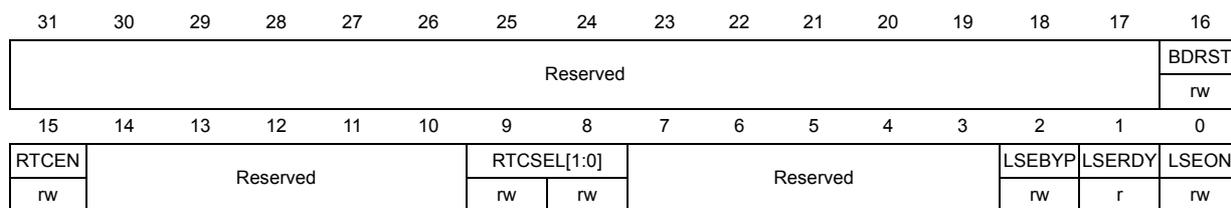
| 31 | 30 | 29 | 28 | 27 | 26 | 25 | 24 | 23 | 22 | 21 | 20 | 19 | 18 | 17 | 16 |
| Reserved | BDRST | ||||||||||||||
| rw | |||||||||||||||
| 15 | 14 | 13 | 12 | 11 | 10 | 9 | 8 | 7 | 6 | 5 | 4 | 3 | 2 | 1 | 0 |
| RTCCEN | Reserved | RTCSEL[1:0] | Reserved | LSEBYP | LSERDY | LSEON | |||||||||
| rw | rw | rw | r | rw | |||||||||||
Bits 31:17 Reserved, always read as 0.
Bit 16 BDRST : Backup domain software reset
Set and cleared by software.
0: Reset not activated
1: Resets the entire Backup domain
Note: The BKPSRAM is not affected by this reset, the only way of resetting the BKPSRAM is through the Flash interface when a protection level change from level 1 to level 0 is requested.
Bit 15 RTCCEN : RTC clock enable
Set and cleared by software.
0: RTC clock disabled
1: RTC clock enabled
Bits 14:10 Reserved, always read as 0.
Bits 9:8 RTCSEL[1:0] : RTC clock source selection
Set by software to select the clock source for the RTC. Once the RTC clock source has been selected, it cannot be changed anymore unless the Backup domain is reset. The BDRST bit can be used to reset them.
00: No clock
01: LSE oscillator clock used as the RTC clock
10: LSI oscillator clock used as the RTC clock
11: HSE oscillator clock divided by a programmable prescaler (selection through the RTCPRE[4:0] bits in the RCC clock configuration register (RCC_CFGR)) used as the RTC clock
Bits 7:3 Reserved, always read as 0.
Bit 2 LSEBYP : External low-speed oscillator bypass
Set and cleared by software to bypass oscillator. This bit can be written only when the LSE clock is disabled.
0: LSE oscillator not bypassed
1: LSE oscillator bypassed
Bit 1 LSERDY : External low-speed oscillator ready
Set and cleared by hardware to indicate when the external 32 kHz oscillator is stable. After the LSEON bit is cleared, LSERDY goes low after 6 external low-speed oscillator clock cycles.
0: LSE clock not ready
1: LSE clock ready
Bit 0 LSEON : External low-speed oscillator enable
Set and cleared by software.
0: LSE clock OFF
1: LSE clock ON
5.3.21 RCC clock control & status register (RCC_CSR)
Address offset: 0x74
Reset value: 0x0E00 0000, reset by system reset, except reset flags by power reset only.
Access: \( 0 \leq \text{wait state} \leq 3 \) , word, half-word and byte access
Wait states are inserted in case of successive accesses to this register.
| 31 | 30 | 29 | 28 | 27 | 26 | 25 | 24 | 23 | 22 | 21 | 20 | 19 | 18 | 17 | 16 |
|---|---|---|---|---|---|---|---|---|---|---|---|---|---|---|---|
| LPWR RSTF | WWDG RSTF | IWDG RSTF | SFT RSTF | POR RSTF | PIN RSTF | BORRS TF | RMVF | Reserved | |||||||
| rw | rw | rw | rw | rw | rw | rw | rw | ||||||||
| 15 | 14 | 13 | 12 | 11 | 10 | 9 | 8 | 7 | 6 | 5 | 4 | 3 | 2 | 1 | 0 |
| Reserved | LSIRDY | LSION | |||||||||||||
| r | rw | ||||||||||||||
Bit 31 LPWRRSTF: Low-power reset flag
Set by hardware when a Low-power management reset occurs.
Cleared by writing to the RMVF bit.
0: No Low-power management reset occurred
1: Low-power management reset occurred
For further information on Low-power management reset, refer to Low-power management reset .
Bit 30 WWDGRSTF: Window watchdog reset flag
Set by hardware when a window watchdog reset occurs.
Cleared by writing to the RMVF bit.
0: No window watchdog reset occurred
1: Window watchdog reset occurred
Bit 29 IWDGRSTF: Independent watchdog reset flag
Set by hardware when an independent watchdog reset from \( V_{DD} \) domain occurs.
Cleared by writing to the RMVF bit.
0: No watchdog reset occurred
1: Watchdog reset occurred
Bit 28 SFTRSTF: Software reset flag
Set by hardware when a software reset occurs.
Cleared by writing to the RMVF bit.
0: No software reset occurred
1: Software reset occurred
Bit 27 PORRSTF: POR/PDR reset flag
Set by hardware when a POR/PDR reset occurs.
Cleared by writing to the RMVF bit.
0: No POR/PDR reset occurred
1: POR/PDR reset occurred
Bit 26 PINRSTF: PIN reset flag
Set by hardware when a reset from the NRST pin occurs.
Cleared by writing to the RMVF bit.
0: No reset from NRST pin occurred
1: Reset from NRST pin occurred
Bit 25 BORRSTF : BOR reset flag
Cleared by software by writing the RMVF bit.
Set by hardware when a POR/PDR or BOR reset occurs.
0: No POR/PDR or BOR reset occurred
1: POR/PDR or BOR reset occurred
Bit 24 RMVF : Remove reset flag
Set by software to clear the reset flags.
0: No effect
1: Clear the reset flags
Bits 23:2 Reserved, always read as 0.
Bit 1 LSIRDY : Internal low-speed oscillator ready
Set and cleared by hardware to indicate when the internal RC 40 kHz oscillator is stable.
After the LSION bit is cleared, LSIRDY goes low after 3 LSI clock cycles.
0: LSI RC oscillator not ready
1: LSI RC oscillator ready
Bit 0 LSION : Internal low-speed oscillator enable
Set and cleared by software.
0: LSI RC oscillator OFF
1: LSI RC oscillator ON
5.3.22 RCC spread spectrum clock generation register (RCC_SSCGR)
Address offset: 0x80
Reset value: 0x0000 0000
Access: no wait state, word, half-word and byte access.
The spread spectrum clock generation is available only for the main PLL.
The RCC_SSCGR register must be written either before the main PLL is enabled or after the main PLL disabled.
Note: For full details about PLL spread spectrum clock generation (SSCG) characteristics, refer to the “Electrical characteristics” section in your device datasheet.
| 31 | 30 | 29 | 28 | 27 | 26 | 25 | 24 | 23 | 22 | 21 | 20 | 19 | 18 | 17 | 16 |
|---|---|---|---|---|---|---|---|---|---|---|---|---|---|---|---|
| SSCG EN | SPR EAD SEL | Reserved | INCSTEP | ||||||||||||
| rw | rw | rw | rw | rw | rw | rw | rw | rw | rw | rw | rw | rw | |||
| 15 | 14 | 13 | 12 | 11 | 10 | 9 | 8 | 7 | 6 | 5 | 4 | 3 | 2 | 1 | 0 |
| INCSTEP | MODPER | ||||||||||||||
| rw | rw | rw | rw | rw | rw | rw | rw | rw | rw | rw | rw | rw | rw | rw | rw |
Bits 31 SSCGEN : Spread spectrum modulation enable
Set and cleared by software.
0: Spread spectrum modulation DISABLE. (To write after clearing CR[24]=PLLON bit)
1: Spread spectrum modulation ENABLE. (To write before setting CR[24]=PLLON bit)
Bit 30 SPREADSEL : Spread Select
Set and cleared by software.
To write before to set CR[24]=PLLON bit.
0: Center spread
1: Down spread
Bit 29:28 Reserved
Bit 27:13 INCSTEP : Incrementation step
Set and cleared by software. To write before setting CR[24]=PLLON bit.
Configuration input for modulation profile amplitude.
Bit 12:0 MODPER : Modulation period
Set and cleared by software. To write before setting CR[24]=PLLON bit.
Configuration input for modulation profile period.
5.3.23 RCC PLLI2S configuration register (RCC_PLLI2SCFGR)
Address offset: 0x84
Reset value: 0x2000 3000
Access: no wait state, word, half-word and byte access.
This register is used to configure the PLLI2S clock outputs according to the formulas:
- • \( f_{(VCO\ clock)} = f_{(PLLI2S\ clock\ input)} \times (PLLI2SN / PLLM) \)
- • \( f_{(PLL\ I2S\ clock\ output)} = f_{(VCO\ clock)} / PLLI2SR \)
| 31 | 30 | 29 | 28 | 27 | 26 | 25 | 24 | 23 | 22 | 21 | 20 | 19 | 18 | 17 | 16 |
|---|---|---|---|---|---|---|---|---|---|---|---|---|---|---|---|
| Reserved | PLLI2S R2 | PLLI2S R1 | PLLI2S R0 | Reserved | |||||||||||
| rw | rw | rw | |||||||||||||
| 15 | 14 | 13 | 12 | 11 | 10 | 9 | 8 | 7 | 6 | 5 | 4 | 3 | 2 | 1 | 0 |
| Reserved | PLLI2SN 8 | PLLI2SN 7 | PLLI2SN 6 | PLLI2SN 5 | PLLI2SN 4 | PLLI2SN 3 | PLLI2SN 2 | PLLI2SN 1 | PLLI2SN 0 | Reserved | |||||
| rw | rw | rw | rw | rw | rw | rw | rw | rw | |||||||
Bit 31 Reserved, always read as 0.
Bits 30:28 PLLI2SR : PLLI2S division factor for I2S clocks
Set and cleared by software to control the I2S clock frequency. These bits should be written only if the PLLI2S is disabled. The factor must be chosen in accordance with the prescaler values inside the I2S peripherals, to reach 0.3% error when using standard crystals and 0% error with audio crystals. For more information about I2S clock frequency and precision, refer to Section 25.4.3: Clock generator in the I2S chapter.
Caution: The I2Ss requires a frequency lower than or equal to 192 MHz to work correctly.
I2S clock frequency = VCO frequency / PLLR with \( 2 \leq PLLR \leq 7 \)
000: PLLR = 0, wrong configuration
001: PLLR = 1, wrong configuration
010: PLLR = 2
...
111: PLLR = 7
Bits 27:15 Reserved, always read as 0.
Bits 14:6 PLLI2SN : PLLI2S multiplication factor for VCO
Set and cleared by software to control the multiplication factor of the VCO. These bits can be written only when the PLLI2S is disabled. Only half-word and word accesses are allowed to write these bits.
Caution: The software has to set these bits correctly to ensure that the VCO output frequency is between 192 and 432 MHz.
VCO output frequency = VCO input frequency \( \times \) PLLI2SN with \( 192 \leq \text{PLLI2SN} \leq 432 \)
000000000: PLLI2SN = 0, wrong configuration
000000001: PLLI2SN = 1, wrong configuration
...
011000000: PLLI2SN = 192
011000001: PLLI2SN = 193
011000010: PLLI2SN = 194
...
110110000: PLLI2SN = 432
110110000: PLLI2SN = 433, wrong configuration
...
111111111: PLLI2SN = 511, wrong configuration
Bits 5:0 Reserved, always read as 0.
5.3.24 RCC register map
Table 13 gives the register map and reset values.
Table 13. RCC register map and reset values
| Addr. offset | Register name | 31 | 30 | 29 | 28 | 27 | 26 | 25 | 24 | 23 | 22 | 21 | 20 | 19 | 18 | 17 | 16 | 15 | 14 | 13 | 12 | 11 | 10 | 9 | 8 | 7 | 6 | 5 | 4 | 3 | 2 | 1 | 0 | |
|---|---|---|---|---|---|---|---|---|---|---|---|---|---|---|---|---|---|---|---|---|---|---|---|---|---|---|---|---|---|---|---|---|---|---|
| 0x00 | RCC_CR | Reserved | PLL I2SRDY | PLL I2SON | PLL RDY | Reserved | CSSON | HSEBYP | HSE RDY | HSEON | HSICAL 7 | HSICAL 6 | HSICAL 5 | HSICAL 4 | HSICAL 3 | HSICAL 2 | HSICAL 1 | HSICAL 0 | HSITRIM 4 | HSITRIM 3 | HSITRIM 2 | HSITRIM 1 | HSITRIM 0 | Reserved | HSIRDY | HSION | ||||||||
| 0x04 | RCC_PLLC FGR | Reserved | PLLQ 3 | PLLQ 2 | PLLQ 1 | PLLQ 0 | Reserved | PLLSPC | Reserved | PLL1 1 | PLL1 0 | Reserved | PLLN 8 | PLLN 7 | PLLN 6 | PLLN 5 | PLLN 4 | PLLN 3 | PLLN 2 | PLLN 1 | PLLN 0 | PLL M 5 | PLL M 4 | PLL M 3 | PLL M 2 | PLL M 1 | PLL M 0 | |||||||
| 0x08 | RCC_CFGR | MCO2 1 | MCO2 0 | MCO2PRE2 | MCO2PRE1 | MCO2PRE0 | MCO1PRE2 | MCO1PRE1 | MCO1PRE0 | I2SSRC | MCO1 1 | MCO1 0 | RTCPRE 4 | RTCPRE 3 | RTCPRE 2 | RTCPRE 1 | RTCPRE 0 | PPRE2 2 | PPRE2 1 | PPRE2 0 | PPRE1 2 | PPRE1 1 | PPRE1 0 | Reserved | HPRE 3 | HPRE 2 | HPRE 1 | HPRE 0 | SWS 1 | SWS 0 | SW 1 | SW 0 | ||
| 0x0C | RCC_CIR | Reserved | CSSC | Reserved | PLL I2SRDYC | PLL RDYC | HSE RDYC | HSIRDYC | LSERDYC | LSIRDYC | Reserved | PLL I2SRDYIE | PLL RDYIE | HSERDYIE | HSIRDYIE | LSERDYIE | LSIRDYIE | CSSF | Reserved | PLL I2SRDYIF | PLL RDYIF | HSERDYIF | HSIRDYIF | LSERDYIF | LSIRDYIF | |||||||||
| 0x10 | RCC_AHB1 RSTR | Reserved | OTGHSRST | Reserved | ETHMACRST | Reserved | DMA2RST | DMA1RST | Reserved | CRCRST | Reserved | GPIOIRST | GPIOHRST | GPIOGRST | GPIOFRST | GPIOERST | GPIODRST | GPIOCRST | GPIOBRST | GPIOARST | ||||||||||||||
| 0x14 | RCC_AHB2 RSTR | Reserved | OTGFSRST | RNGRST | HSAHRST | CRYPRST | Reserved | DCMIRST | ||||||||||||||||||||||||||
| 0x18 | RCC_AHB3 RSTR | Reserved | FSMCRST | |||||||||||||||||||||||||||||||
| 0x1C | Reserved | Reserved | ||||||||||||||||||||||||||||||||
| 0x20 | RCC_APB1 RSTR | Reserved | DACRST | PWRRST | Reserved | CAN2RST | CAN1RST | Reserved | I2C3RST | I2C2RST | I2C1RST | UART5RST | UART4RST | UART3RST | UART2RST | Reserved | SPI3RST | SPI2RST | Reserved | WWDGRST | Reserved | TIM14RST | TIM13RST | TIM12RST | TIM7RST | TIM6RST | TIM5RST | TIM4RST | ||||||
| 0x24 | RCC_APB2 RSTR | Reserved | TIM11RST | TIM10RST | TIM9RST | Reserved | SYSCFGGRST | Reserved | SP1RST | SDIORST | Reserved | ADCIRST | Reserved | USART6RST | USART1RST | Reserved | ||||||||||||||||||
| 0x28 | Reserved | Reserved | ||||||||||||||||||||||||||||||||
| 0x2C | Reserved | Reserved | ||||||||||||||||||||||||||||||||
| 0x30 | RCC_AHB1 ENR | Reserved | OTGHSULPIEN | OTGHSEN | ETHMACPTPEN | ETHMACRXEN | ETHMACTXEN | ETHMACEN | Reserved | DMA2EN | DMA1EN | Reserved | BKPSRAMEN | Reserved | CRCEN | Reserved | GPIOEN | GPIOHEN | GPIOGEN | GPIOFEN | GPIOEEN | GPIODEN | GPIOCEN | GPIOBEN | GPIOAEN | |||||||||
Table 13. RCC register map and reset values (continued)
| Addr. offset | Register name | 31 | 30 | 29 | 28 | 27 | 26 | 25 | 24 | 23 | 22 | 21 | 20 | 19 | 18 | 17 | 16 | 15 | 14 | 13 | 12 | 11 | 10 | 9 | 8 | 7 | 6 | 5 | 4 | 3 | 2 | 1 | 0 |
|---|---|---|---|---|---|---|---|---|---|---|---|---|---|---|---|---|---|---|---|---|---|---|---|---|---|---|---|---|---|---|---|---|---|
| 0x34 | RCC_AHB2 ENR | OTGFSEN | RNGEN | HASHEN | CRYPEN | Reserved | DCMIEN | ||||||||||||||||||||||||||
| 0x38 | RCC_AHB3 ENR | FSMCGEN | |||||||||||||||||||||||||||||||
| 0x3C | Reserved | ||||||||||||||||||||||||||||||||
| 0x40 | RCC_APB1 ENR | Reserved | DACEN | PWREN | Reserved | CAN2EN | CAN1EN | Reserved | I2C3EN | I2C2EN | I2C1EN | UART5EN | UART4EN | USART3EN | USART2EN | Reserved | SPI3EN | SPI2EN | Reserved | WWDGEN | Reserved | TIM14EN | TIM13EN | TIM12EN | TIM7EN | TIM6EN | TIM5EN | TIM4EN | TIM3EN | TIM2EN | |||
| 0x44 | RCC_APB2 ENR | TIM11EN | TIM10EN | TIM9EN | Reserved | SYSCFGEN | Reserved | SPI1EN | SDIOEN | ADC3EN | ADC2EN | ADC1EN | Reserved | USART6EN | USART1EN | Reserved | TIM8EN | TIM1EN | |||||||||||||||
| 0x48 | Reserved | ||||||||||||||||||||||||||||||||
| 0x4C | Reserved | ||||||||||||||||||||||||||||||||
| 0x50 | RCC_AHB1 LPENR | Reserved | OTGHSULPILPEN | OTGHSLPEN | ETHMACPTLPEN | ETHMACRXLPEN | ETHMACTXLPEN | ETHMACCLPEN | Reserved | DMA2LPEN | DMA1LPEN | Reserved | BKPSRAMLPEN | SRAM2LPEN | SRAM1LPEN | FLITLPEN | Reserved | CRCLPEN | Reserved | GPIOILPEN | GPIOHLPEN | GPIOGLPEN | GPIOFLPEN | GPIOELPEN | GPIOILPEN | GPIOHLPEN | GPIOGLPEN | GPIOFLPEN | GPIOELPEN | GPIOILPEN | GPIOHLPEN | GPIOGLPEN | GPIOALPEN |
| 0x54 | RCC_AHB2 LPENR | OTGFSLPEN | RNGLPEN | HASHLPEN | CRYPLPEN | Reserved | DCMILPEN | ||||||||||||||||||||||||||
| 0x58 | RCC_AHB3 LPENR | FSMCLPEN | |||||||||||||||||||||||||||||||
| 0x5C | Reserved | ||||||||||||||||||||||||||||||||
| 0x60 | RCC_APB1 LPENR | Reserved | DACLPEN | PWRLPEN | Reserved | CAN2LPEN | CAN1LPEN | Reserved | I2C3LPEN | I2C2LPEN | I2C1LPEN | UART5LPEN | UART4LPEN | USART3LPEN | USART2LPEN | Reserved | SPI3LPEN | SPI2LPEN | Reserved | WWDGLPEN | Reserved | TIM14LPEN | TIM13LPEN | TIM12LPEN | TIM7LPEN | TIM6LPEN | TIM5LPEN | TIM4LPEN | TIM3LPEN | TIM2LPEN | |||
| 0x64 | RCC_APB2 LPENR | TIM11LPEN | TIM10LPEN | TIM9LPEN | Reserved | SYSCFGLPEN | Reserved | SPI1LPEN | SDIOLPEN | ADC3LPEN | ADC2LPEN | ADC1LPEN | Reserved | USART6LPEN | USART1LPEN | Reserved | TIM8LPEN | TIM1LPEN | |||||||||||||||
| 0x68 | Reserved | ||||||||||||||||||||||||||||||||
| 0x6C | Reserved | ||||||||||||||||||||||||||||||||
| 0x70 | RCC_BDCR | BDRST | RTCEN | Reserved | RTCSEL 1 | RTCSEL 0 | Reserved | LSEBYP | LSERDY | LSEON |
Table 13. RCC register map and reset values (continued)
| Addr. offset | Register name | 31 | 30 | 29 | 28 | 27 | 26 | 25 | 24 | 23 | 22 | 21 | 20 | 19 | 18 | 17 | 16 | 15 | 14 | 13 | 12 | 11 | 10 | 9 | 8 | 7 | 6 | 5 | 4 | 3 | 2 | 1 | 0 |
|---|---|---|---|---|---|---|---|---|---|---|---|---|---|---|---|---|---|---|---|---|---|---|---|---|---|---|---|---|---|---|---|---|---|
| 0x74 | RCC_CSR | LPWRRSTF | WWDGRSTF | IWDGRSTF | SFTRSTF | PORRSTF | PADRSTF | BORRSTF | RMVF | Reserved | LSIRDY | LSION | |||||||||||||||||||||
| 0x78 | Reserved | Reserved | |||||||||||||||||||||||||||||||
| 0x7C | Reserved | Reserved | |||||||||||||||||||||||||||||||
| 0x80 | RCC_SSCGR | SSCGEN | SPREADSEL | Reserved | INCSTEP | MODPER | |||||||||||||||||||||||||||
| 0x84 | RCC_PLLI2SCFGR | Reserved | PLLI2SRx | Reserved | PLLI2SNx | Reserved | |||||||||||||||||||||||||||
Refer to Section 2.3 on page 51 for the register boundary addresses.