2. Memory and bus architecture
2.1 System architecture
The main system consists of 32-bit multilayer AHB bus matrix that interconnects:
- • Height masters:
- – Cortex ® -M3 core I-bus, D-bus and S-bus
- – DMA1 memory bus
- – DMA2 memory bus
- – DMA2 peripheral bus
- – Ethernet DMA bus
- – USB OTG HS DMA bus
- • Seven slaves:
- – Internal Flash memory ICode bus
- – Internal Flash memory DCode bus
- – Main internal SRAM1 (112 KB)
- – Auxiliary internal SRAM2 (16 KB)
- – AHB1peripherals including AHB to APB bridges and APB peripherals
- – AHB2 peripherals
- – FSMC
The bus matrix provides access from a master to a slave, enabling concurrent access and efficient operation even when several high-speed peripherals work simultaneously. This architecture is shown in Figure 1 .
Figure 1. System architecture
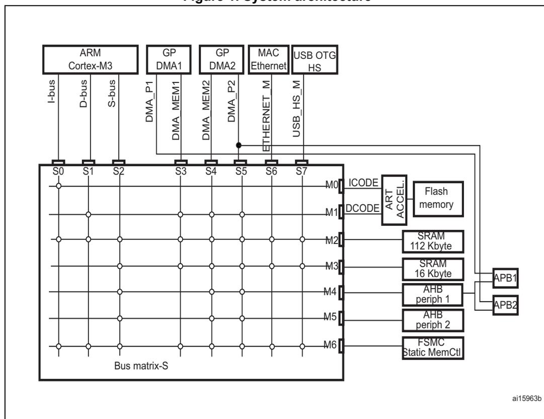
The diagram illustrates the system architecture of the RM0033 microcontroller. At the top, the ARM Cortex-M3 core is shown with its I-bus, D-bus, and S-bus connected to the Bus matrix-S. Below the core, two General Purpose DMA (GP DMA) units, DMA1 and DMA2, are shown with their respective master interfaces (DMA_P1, DMA_MEM1, DMA_MEM2, DMA_P2) connected to the matrix. A MAC Ethernet and a USB OTG HS are also connected to the matrix via their master interfaces (ETHERNET_M and USB_HS_M). The Bus matrix-S is a grid with 8 slave ports (S0 to S7) on the left and 7 master ports (M0 to M6) on the right. The slave ports are connected to the ARM Cortex-M3 (S0, S1, S2), GP DMA1 (S3), GP DMA2 (S4), MAC Ethernet (S5), and USB OTG HS (S6, S7). The master ports are connected to various system components: M0 (ICODE) and M1 (DCODE) lead to an ART ACCEL block, which is connected to Flash memory; M2 is connected to SRAM 112 Kbyte; M3 is connected to SRAM 16 Kbyte; M4 is connected to AHB periph 1; M5 is connected to AHB periph 2; and M6 is connected to FSMC Static MemCtl. APB1 and APB2 are shown as being connected to AHB periph 1. The diagram is labeled 'ai15963b' in the bottom right corner.
2.1.1 S0: I-bus
This bus connects the Instruction bus of the Cortex ® -M3 core to the BusMatrix. This bus is used by the core to fetch instructions. The target of this bus is a memory containing code (internal Flash memory/SRAM or external memories through the FSMC).
2.1.2 S1: D-bus
This bus connects the databus of the Cortex ® -M3 to the BusMatrix. This bus is used by the core for literal load and debug access. The target of this bus is a memory containing code or data (internal Flash memory /SRAM or external memories through the FSMC).
2.1.3 S2: S-bus
This bus connects the system bus of the Cortex ® -M3 core to a BusMatrix. This bus is used to access data located in a peripheral or in SRAM. Instructions may also be fetch on this bus (less efficient than ICode). The targets of this bus are the 112 KB & 16 KB internal SRAMs, the AHB1 peripherals including the APB peripherals, the AHB2 peripherals and the external memories through the FSMC.
2.1.4 S3, S4: DMA memory bus
This bus connects the DMA memory bus master interface to the BusMatrix. It is used by the DMA to perform transfer to/from memories. The targets of this bus are data memories: internal SRAM and external memories through the FSMC.
2.1.5 S5: DMA peripheral bus
This bus connects the DMA peripheral master bus interface to the BusMatrix. This bus is used by the DMA to access AHB peripherals or to perform memory-to-memory transfers. The targets of this bus are the AHB and APB peripherals plus data memories: internal SRAM and external memories through the FSMC.
2.1.6 S6: Ethernet DMA bus
This bus connects the Ethernet DMA master interface to the BusMatrix. This bus is used by the Ethernet DMA to load/store data to a memory. The targets of this bus are data memories: internal SRAM and external memories through the FSMC.
2.1.7 S7: USB OTG HS DMA bus
This bus connects the USB OTG HS DMA master interface to the BusMatrix. This bus is used by the USB OTG DMA to load/store data to a memory. The targets of this bus are data memories: internal SRAM and external memories through the FSMC.
2.1.8 BusMatrix
The BusMatrix manages the access arbitration between masters. The arbitration uses a round-robin algorithm.
2.1.9 AHB/APB bridges (APB)
The two AHB/APB bridges provide full synchronous connections between the AHB and the two APB buses, allowing flexible selection of the peripheral frequency:
- • APB1, limited to 30 MHz for low-speed peripherals
- • APB2, limited to 60 MHz for high-speed peripherals
Refer to Table 1 on page 51 for the address mapping of AHB and APB peripherals.
After each device reset, all peripheral clocks are disabled (except for the SRAM and Flash memory interface). Before using a peripheral you have to enable its clock in the RCC_AHBxENR or RCC_APBxENR register.
Note: When a 16- or an 8-bit access is performed on an APB register, the access is transformed into a 32-bit access: the bridge duplicates the 16- or 8-bit data to feed the 32-bit vector.
2.2 Memory organization
Program memory, data memory, registers and I/O ports are organized within the same linear 4 Gbyte address space.
The bytes are coded in memory in little endian format. The lowest numbered byte in a word is considered the word's least significant byte and the highest numbered byte, the word's most significant.
For the detailed mapping of peripheral registers, refer to the related chapters.
The addressable memory space is divided into 8 main blocks, each of 512 MB.
All the memory areas that are not allocated to on-chip memories and peripherals are considered "Reserved"). Refer to the memory map figure in the product datasheet.
2.3 Memory map
See the datasheet corresponding to your device for a comprehensive diagram of the memory map. Table 1 gives the boundary addresses of the peripherals available in all STM32F20x and STM32F21x devices.
Table 1. STM32F20x and STM32F21x register boundary addresses
| Boundary address | Peripheral | Bus | Register map |
|---|---|---|---|
| 0xA000 0000 - 0xA000 0FFF | FSMC control register | AHB3 | Section 31.6.9: FSMC register map on page 1299 |
| 0x5006 0800 - 0x5006 0BFF | RNG | AHB2 | Section 20.4.4: RNG register map on page 539 |
| 0x5006 0400 - 0x5006 07FF | HASH | Section 21.4.8: HASH register map on page 559 | |
| 0x5006 0000 - 0x5006 03FF | CRYP | Section 19.6.11: CRYP register map on page 533 | |
| 0x5005 0000 - 0x5005 03FF | DCMI | Section 12.8.12: DCMI register map on page 296 | |
| 0x5000 0000 - 0x5003 FFFF | USB OTG FS | Section 29.16.6: OTG_FS register map on page 1025 | |
| 0x4004 0000 - 0x4007 FFFF | USB OTG HS | Section 30.12.6: OTG_HS register map on page 1171 | |
| 0x4002 9000 - 0x4002 93FF | ETHERNET MAC | Section 28.8.5: Ethernet register maps on page 935 | |
| 0x4002 8C00 - 0x4002 8FFF | |||
| 0x4002 8800 - 0x4002 8BFF | |||
| 0x4002 8400 - 0x4002 87FF | |||
| 0x4002 8000 - 0x4002 83FF | |||
| 0x4002 6400 - 0x4002 67FF | DMA2 | Section 9.5.11: DMA register map on page 205 | |
| 0x4002 6000 - 0x4002 63FF | DMA1 | ||
| 0x4002 4000 - 0x4002 4FFF | BKPSRAM | ||
| 0x4002 3C00 - 0x4002 3FFF | Flash interface register | AHB1 | See Flash programming manual |
| 0x4002 3800 - 0x4002 3BFF | RCC | Section 5.3.24: RCC register map on page 132 | |
| 0x4002 3000 - 0x4002 33FF | CRC | Section 3.4.4: CRC register map on page 63 | |
| 0x4002 2000 - 0x4002 23FF | GPIOI | Section 6.4.11: GPIO register map on page 154 | |
| 0x4002 1C00 - 0x4002 1FFF | GPIOH | ||
| 0x4002 1800 - 0x4002 1BFF | GPIOG | ||
| 0x4002 1400 - 0x4002 17FF | GPIOF | ||
| 0x4002 1000 - 0x4002 13FF | GPIOE | ||
| 0x4002 0C00 - 0x4002 0FFF | GPIO_D | ||
| 0x4002 0800 - 0x4002 0BFF | GPIOC | ||
| 0x4002 0400 - 0x4002 07FF | GPIOB | ||
| 0x4002 0000 - 0x4002 03FF | GPIOA |
Table 1. STM32F20x and STM32F21x register boundary addresses (continued)
| Boundary address | Peripheral | Bus | Register map |
|---|---|---|---|
| 0x4001 4800 - 0x4001 4BFF | TIM11 | APB2 | Section 15.5.12: TIM10/11/13/14 register map on page 473 |
| 0x4001 4400 - 0x4001 47FF | TIM10 | ||
| 0x4001 4000 - 0x4001 43FF | TIM9 | Section 15.4.14: TIM9/12 register map on page 463 | |
| 0x4001 3C00 - 0x4001 3FFF | EXTI | Section 8.3.7: EXTI register map on page 172 | |
| 0x4001 3800 - 0x4001 3BFF | SYSCFG | Section 7.2.8: SYSCFG register map on page 160 | |
| 0x4001 3000 - 0x4001 33FF | SPI1 | Section 25.5.10: SPI register map on page 723 | |
| 0x4001 2C00 - 0x4001 2FFF | SDIO | Section 26.9.16: SDIO register map on page 778 | |
| 0x4001 2000 - 0x4001 23FF | ADC1 - ADC2 - ADC3 | Section 10.13.18: ADC register map on page 250 | |
| 0x4001 1400 - 0x4001 17FF | USART6 | Section 24.6.8: USART register map on page 671 | |
| 0x4001 1000 - 0x4001 13FF | USART1 | ||
| 0x4001 0400 - 0x4001 07FF | TIM8 | Section 13.4.21: TIM1 and TIM8 register map on page 366 | |
| 0x4001 0000 - 0x4001 03FF | TIM1 |
Table 1. STM32F20x and STM32F21x register boundary addresses (continued)
| Boundary address | Peripheral | Bus | Register map |
|---|---|---|---|
| 0x4000 7400 - 0x4000 77FF | DAC | APB1 | Section 11.5.15: DAC register map on page 273 |
| 0x4000 7000 - 0x4000 73FF | PWR | Section 4.4.3: PWR register map on page 83 | |
| 0x4000 6800 - 0x4000 6BFF | CAN2 | Section 27.9.5: bxCAN register map on page 819 | |
| 0x4000 6400 - 0x4000 67FF | CAN1 | ||
| 0x4000 5C00 - 0x4000 5FFF | I2C3 | Section 23.6.10: I2C register map on page 619 | |
| 0x4000 5800 - 0x4000 5BFF | I2C2 | ||
| 0x4000 5400 - 0x4000 57FF | I2C1 | ||
| 0x4000 5000 - 0x4000 53FF | UART5 | Section 24.6.8: USART register map on page 671 | |
| 0x4000 4C00 - 0x4000 4FFF | UART4 | ||
| 0x4000 4800 - 0x4000 4BFF | USART3 | ||
| 0x4000 4400 - 0x4000 47FF | USART2 | ||
| 0x4000 3C00 - 0x4000 3FFF | SPI3 / I2S3 | Section 25.5.10: SPI register map on page 723 | |
| 0x4000 3800 - 0x4000 3BFF | SPI2 / I2S2 | ||
| 0x4000 3000 - 0x4000 33FF | IWDG | Section 17.4.5: IWDG register map on page 491 | |
| 0x4000 2C00 - 0x4000 2FFF | WWDG | Section 18.6.4: WWDG register map on page 498 | |
| 0x4000 2800 - 0x4000 2BFF | RTC & BKP Registers | Section 22.6.15: RTC register map on page 587 | |
| 0x4000 2000 - 0x4000 23FF | TIM14 | Section 15.5.12: TIM10/11/13/14 register map on page 473 | |
| 0x4000 1C00 - 0x4000 1FFF | TIM13 | ||
| 0x4000 1800 - 0x4000 1BFF | TIM12 | Section 15.4.14: TIM9/12 register map on page 463 | |
| 0x4000 1400 - 0x4000 17FF | TIM7 | Section 16.4.9: TIM6 and TIM7 register map on page 486 | |
| 0x4000 1000 - 0x4000 13FF | TIM6 | ||
| 0x4000 0C00 - 0x4000 0FFF | TIM5 | Section 14.4.21: TIMx register map on page 426 | |
| 0x4000 0800 - 0x4000 0BFF | TIM4 | ||
| 0x4000 0400 - 0x4000 07FF | TIM3 | ||
| 0x4000 0000 - 0x4000 03FF | TIM2 |
2.3.1 Embedded SRAM
The STM32F20x and STM32F21x feature 4 Kbytes of backup SRAM (see Section 4.1.2: Battery backup domain ) plus 128 Kbytes of system SRAM.
The system SRAM can be accessed as bytes, half-words (16 bits) or full words (32 bits). The start address of the SRAM is 0x2000 0000. Read and write operations are performed at CPU speed with 0 wait state.
The system SRAM is split up into two blocks, of 112 KB and 16 KB, with a capability for concurrent access from by the AHB masters (like the Ethernet or the USB OTG HS): for
instance, the Ethernet MAC can read/write from/to the 16 KB SRAM while the CPU is reading/writing from/to the 112 KB SRAM.
The CPU can access the system SRAM through the System Bus or through the I-Code/D-Code buses when boot from SRAM is selected or when physical remap is selected ( SYSCFG memory remap register (SYSCFG_MEMRMP) in the SYSCFG controller). To get the max performance on SRAM execution, physical remap should be selected (boot or software selection).
2.3.2 Bit banding
The Cortex ® -M3 memory map includes two bit-band regions. These regions map each word in an alias region of memory to a bit in a bit-band region of memory. Writing to a word in the alias region has the same effect as a read-modify-write operation on the targeted bit in the bit-band region.
In the STM32F20x and STM32F21x both the peripheral registers and the SRAM are mapped to a bit-band region, so that single bit-band write and read operations are allowed. The operations are only available for Cortex ® -M3 accesses, and not from other bus masters (e.g. DMA).
A mapping formula shows how to reference each word in the alias region to a corresponding bit in the bit-band region. The mapping formula is:
where:
- – bit_word_addr is the address of the word in the alias memory region that maps to the targeted bit
- – bit_band_base is the starting address of the alias region
- – byte_offset is the number of the byte in the bit-band region that contains the targeted bit
- – bit_number is the bit position (0-7) of the targeted bit
Example
The following example shows how to map bit 2 of the byte located at SRAM address 0x20000300 to the alias region:
Writing to address 0x22006008 has the same effect as a read-modify-write operation on bit 2 of the byte at SRAM address 0x20000300.
Reading address 0x22006008 returns the value (0x01 or 0x00) of bit 2 of the byte at SRAM address 0x20000300 (0x01: bit set; 0x00: bit reset).
For more information on bit-banding, refer to the Cortex ® -M3 programming manual (see Related documents on page 1 ).
2.3.3 Embedded Flash memory
The Flash memory has the following main features:
- • Capacity up to 1 Mbyte
- • 128 bits wide data read
- • Byte, half-word, word and double word write
- • Sector and mass erase
- • Memory organization
The Flash memory is organized as follows:
- – A main memory block divided into 4 sectors of 16 Kbytes, 1 sector of 64 Kbytes, and 7 sectors of 128 Kbytes
- – System memory from which the device boots in System memory boot mode
- – 512 OTP (one-time programmable) bytes for user data
The OTP area contains 16 additional bytes used to lock the corresponding OTP data block.
- – Option bytes to configure read and write protection, BOR level, watchdog software/hardware and reset when the device is in Standby or Stop mode
Table 2. Flash module organization
| Block | Name | Block base addresses | Size |
|---|---|---|---|
| Main memory | Sector 0 | 0x0800 0000 - 0x0800 3FFF | 16 Kbyte |
| Sector 1 | 0x0800 4000 - 0x0800 7FFF | 16 Kbyte | |
| Sector 2 | 0x0800 8000 - 0x0800 BFFF | 16 Kbyte | |
| Sector 3 | 0x0800 C000 - 0x0800 FFFF | 16 Kbyte | |
| Sector 4 | 0x0801 0000 - 0x0801 FFFF | 64 Kbyte | |
| Sector 5 | 0x0802 0000 - 0x0803 FFFF | 128 Kbyte | |
| Sector 6 | 0x0804 0000 - 0x0805 FFFF | 128 Kbyte | |
| . | . | . | |
| . | . | . | |
| Sector 11 | 0x080E 0000 - 0x080F FFFF | 128 Kbyte | |
| System memory | 0x1FFF 0000 - 0x1FFF 77FF | 30 Kbyte | |
| OTP | 0x1FFF 7800 - 0x1FFF 7A0F | 528 bytes | |
| Option bytes | 0x1FFF C000 - 0x1FFF C00F | 16 bytes | |
2.3.4 Flash memory read interface
Relation between CPU clock frequency and Flash memory read time
To correctly read data from Flash memory, the number of wait states (LATENCY) must be correctly programmed in the Flash access control register (FLASH_ACR) according to the frequency of the Cortex®-M3 clock and the supply voltage of the device. Table 3 shows the correspondence between wait states and core clock frequency.
Table 3. Number of wait states according to Cortex ® -M3 clock frequency| Wait states (WS) (LATENCY) | HCLK - Cortex ® -M3 clock frequency (MHz) | |||
|---|---|---|---|---|
| Voltage range 2.7 to 3.6 V | Voltage range 2.4 to 2.7 V | Voltage range 2.1 to 2.4 V | Voltage range 1.8 (1) to 2.1 V | |
| 0 WS (1 CPU cycle) | 0 < HCLK ≤ 30 | 0 < HCLK ≤ 24 | 0 < HCLK ≤ 18 | 0 < HCLK ≤ 16 |
| 1 WS (2 CPU cycles) | 30 < HCLK ≤ 60 | 24 < HCLK ≤ 48 | 18 < HCLK ≤ 36 | 16 < HCLK ≤ 32 |
| 2 WS (3 CPU cycles) | 60 < HCLK ≤ 90 | 48 < HCLK ≤ 72 | 36 < HCLK ≤ 54 | 32 < HCLK ≤ 48 |
| 3 WS (4 CPU cycles) | 90 < HCLK ≤ 120 | 72 < HCLK ≤ 96 | 54 < HCLK ≤ 72 | 48 < HCLK ≤ 64 |
| 4 WS (5 CPU cycles) | 96 < HCLK ≤ 120 | 72 < HCLK ≤ 90 | 64 < HCLK ≤ 80 | |
| 5 WS (6 CPU cycles) | 90 < HCLK ≤ 108 | 80 < HCLK ≤ 96 | ||
| 6 WS (7 CPU cycles) | 108 < HCLK ≤ 120 | 96 < HCLK ≤ 112 | ||
| 7 WS (8 CPU cycles) | 112 < HCLK ≤ 120 | |||
1. If IRROFF is set to VDD on STM32F20xx devices, this value can be lowered to 1.65 V when the device operates in a reduced temperature range.
After reset, the CPU clock frequency is 16 MHz and 0 wait state (WS) is configured in the FLASH_ACR register.
It is highly recommended to use the following software sequences to tune the number of wait states needed to access the Flash memory with the CPU frequency.
Increasing the CPU frequency
- • Program the new number of wait states to the LATENCY bits in the FLASH_ACR register
- • Check that the new number of wait states is used to access the Flash memory by reading the FLASH_ACR register
- • Modify the CPU clock source by writing the SW bits in the RCC clock configuration register (RCC_CFGR)
- • If needed, modify the CPU clock prescaler by writing the HPRE bits in RCC_CFGR
- • Check that the new CPU clock source or/and the new CPU clock prescaler value is/are taken into account by reading the clock source status (SWS bits) or/and the AHB prescaler value (HPRE bits), respectively, in the RCC_CFGR register
Decreasing the CPU frequency
- • Modify the CPU clock source by writing the SW bits in the RCC_CFGR register
- • If needed, modify the CPU clock prescaler by writing the HPRE bits in RCC_CFGR
- • Check that the new CPU clock source or/and the new CPU clock prescaler value is/are taken into account by reading the clock source status (SWS bits) or/and the AHB prescaler value (HPRE bits), respectively, in the RCC_CFGR register
- • Program the new number of wait states to the LATENCY bits in FLASH_ACR
- • Check that the new number of wait states is used to access the Flash memory by reading the FLASH_ACR register
Note: A change in CPU clock configuration or wait state (WS) configuration may not be effective straight away. To make sure that the current CPU clock frequency is the one you have
configured, you can check the AHB prescaler factor and clock source status values. To make sure that the number of WS you have programmed is effective, you can read the FLASH_ACR register.
The FLASH_ACR register is used to enable/disable the acceleration features and control the Flash memory access time according to CPU frequency. The tables below provides the bit map and bit descriptions for this register.
For complete information on Flash memory operations and register configurations, refer to the STM32F20x and STM32F21x Flash programming manual (PM0059).
Flash access control register (FLASH_ACR)
The Flash access control register is used to enable/disable the acceleration features and control the Flash memory access time according to CPU frequency.
Address offset: 0x00
Reset value: 0x0000 0000
Access: no wait state, word, half-word and byte access
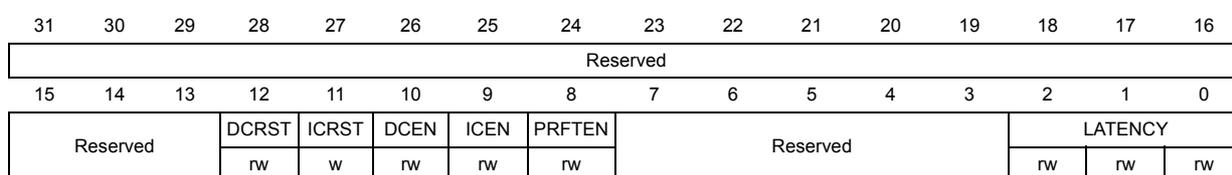
| 31 | 30 | 29 | 28 | 27 | 26 | 25 | 24 | 23 | 22 | 21 | 20 | 19 | 18 | 17 | 16 |
| Reserved | |||||||||||||||
| 15 | 14 | 13 | 12 | 11 | 10 | 9 | 8 | 7 | 6 | 5 | 4 | 3 | 2 | 1 | 0 |
| Reserved | DCRST | ICRST | DCEN | ICEN | PRFTEN | Reserved | LATENCY | ||||||||
| rw | w | rw | rw | rw | rw | rw | rw | ||||||||
Bits 31:11 Reserved, must be kept cleared.
Bit 12 DCRST : Data cache reset
- 0: Data cache is not reset
- 1: Data cache is reset
This bit can be written only when the D cache is disabled.
Bit 11 ICRST : Instruction cache reset
- 0: Instruction cache is not reset
- 1: Instruction cache is reset
This bit can be written only when the I cache is disabled.
Bit 10 DCEN : Data cache enable
- 0: Data cache is disabled
- 1: Data cache is enabled
Bit 9 ICEN : Instruction cache enable
- 0: Instruction cache is disabled
- 1: Instruction cache is enabled
Bit 8 PRFTEN : Prefetch enable
0: Prefetch is disabled
1: Prefetch is enabled
Bits 7:3 Reserved, must be kept cleared.
Bits 2:0 LATENCY : Latency
These bits represent the ratio of the CPU clock period to the Flash memory access time.
000: Zero wait state
001: One wait state
010: Two wait states
011: Three wait states
100: Four wait states
101: Five wait states
110: Six wait states
111: Seven wait states
2.3.5 Adaptive real-time memory accelerator (ART Accelerator™)
The ART Accelerator™ is a memory accelerator which is optimized for STM32 industry-standard Arm® Cortex®-M3 processors. It balances the inherent performance advantage of the Arm® Cortex®-M3 over Flash memory technologies, which normally requires the processor to wait for the Flash memory at higher operating frequencies. Thanks to the ART Accelerator™, the CPU can operate up to 120 MHz without wait states, thereby increasing the overall system speed and efficiency.
To release the processor full 150 DMIPS performance at this frequency the accelerator implements an instruction prefetch queue and branch cache, which enables program execution from Flash memory at up to 120 MHz without wait states.
2.4 Boot configuration
Due to its fixed memory map, the code area starts from address 0x0000 0000 (accessed through the ICode/DCode buses) while the data area (SRAM) starts from address 0x2000 0000 (accessed through the system bus). The Cortex®-M3 CPU always fetches the reset vector on the ICode bus, which implies to have the boot space available only in the code area (typically, Flash memory). STM32F20x and STM32F21x microcontrollers implement a special mechanism to be able to boot from other memories (like the internal SRAM).
In the STM32F20x and STM32F21x, three different boot modes can be selected through the BOOT[1:0] pins as shown in Table 4 .
Table 4. Boot modes
| Boot mode selection pins | Boot mode | Aliasings | |
|---|---|---|---|
| BOOT1 | BOOT0 | ||
| x | 0 | Main Flash memory | Main Flash memory is selected as the boot space |
| 0 | 1 | System memory | System memory is selected as the boot space |
| 1 | 1 | Embedded SRAM | Embedded SRAM is selected as the boot space |
The values on the BOOT pins are latched on the 4th rising edge of SYSCLK after a reset. It is up to the user to set the BOOT1 and BOOT0 pins after reset to select the required boot mode.
BOOT0 is a dedicated pin while BOOT1 is shared with a GPIO pin. Once BOOT1 has been sampled, the corresponding GPIO pin is free and can be used for other purposes.
The BOOT pins are also resampled when the device exits the Standby mode. Consequently, they must be kept in the required Boot mode configuration when the device is in the Standby mode. After this startup delay is over, the CPU fetches the top-of-stack value from address 0x0000 0000, then starts code execution from the boot memory starting from 0x0000 0004.
Note: When the device boots from SRAM, in the application initialization code, you have to relocate the vector table in SRAM using the NVIC exception table and the offset register.
Physical remap
Once the boot pins are selected, the application software can modify the memory accessible in the code area (in this way the code can be executed through the ICode bus in place of the System bus). This modification is performed by programming the Section 7.2.1: SYSCFG memory remap register (SYSCFG_MEMRMP) in the SYSCFG controller.
The following memories can thus be remapped:
- • Main Flash memory
- • System memory
- • Embedded SRAM1 (112 KB)
- • FSMC Bank 1 (NOR/PSRAM 1 and 2)
Table 5. Memory mapping vs. Boot mode/physical remap
| Addresses | Boot/Remap in main Flash memory | Boot/Remap in embedded SRAM | Boot/Remap in System memory | Remap in FSMC |
|---|---|---|---|---|
| 0x2001 C000 - 0x2001 FFFF | SRAM2 (16 KB) | SRAM2 (16 KB) | SRAM2 (16 KB) | SRAM2 (16 KB) |
| 0x2000 0000 - 0x2001 BFFF | SRAM1 (112 KB) | SRAM1 (112 KB) | SRAM1 (112 KB) | SRAM1 (112 KB) |
| 0x1FFF 0000 - 0x1FFF 77FF | System memory | System memory | System memory | System memory |
| 0x0810 0000 - 0x0FFF FFFF | Reserved | Reserved | Reserved | Reserved |
| 0x0800 0000 - 0x080F FFFF | Flash memory | Flash memory | Flash memory | Flash memory |
| 0x0400 0000 - 0x07FF FFFF | Reserved | Reserved | Reserved | FSMC Bank1 NOR/PSRAM 2 (Aliased) |
| 0x0000 0000 - 0x03FF FFFF (1)(2) | Flash (1 MB) Aliased | SRAM1 (112 KB) Aliased | System memory (30 KB) Aliased | FSMC Bank1 NOR/PSRAM 1 (Aliased) |
- 1. When the FSMC is remapped at address 0x0000 0000, only the first two regions of Bank 1 memory controller (Bank1 NOR/PSRAM 1 and NOR/PSRAM 2) can be remapped. In remap mode, the CPU can access the external memory via ICode bus instead of System bus which boosts up the performance. However, in remap mode, the FSMC addressing is fixed to the remap address area only (Bank1 NOR/PSRAM 1 and NOR/PSRAM 2) and FSMC control registers are not accessible. The FSMC remap function must be disabled to allows addressing other memory devices through the FSMC and/or to access FSMC control registers.
- 2. Even when aliased in the boot memory space, the related memory is still accessible at its original memory space.
Embedded bootloader
The embedded bootloader mode is used to reprogram the Flash memory using one of the following serial interfaces:
- • USART1(PA9/PA10)
- • USART3(PB10/11 and PC10/11)
- • CAN2(PB5/13)
- • USB OTG FS(PA11/12) in Device mode (DFU: device firmware upgrade).
The USART peripherals operate at the internal 16 MHz oscillator (HSI) frequency, while the CAN and USB OTG FS require an external clock (HSE) multiple of 1 MHz (ranging from 4 to 26 MHz).
The embedded bootloader code is located in system memory. It is programmed by ST during production. For additional information, refer to application note AN2606.