29. Ethernet (ETH): media access control (MAC) with DMA controller
Low-density devices are STM32F101xx, STM32F102xx and STM32F103xx microcontrollers where the Flash memory density ranges between 16 and 32 Kbytes.
Medium-density devices are STM32F101xx, STM32F102xx and STM32F103xx microcontrollers where the Flash memory density ranges between 64 and 128 Kbytes.
High-density devices are STM32F101xx and STM32F103xx microcontrollers where the Flash memory density ranges between 256 and 512 Kbytes.
XL-density devices are STM32F101xx and STM32F103xx microcontrollers where the Flash memory density ranges between 768 Kbytes and 1 Mbyte.
Connectivity line devices are STM32F105xx and STM32F107xx microcontrollers.
This section applies only to STM32F107xx connectivity line devices.
29.1 Ethernet introduction
Portions Copyright (c) 2004, 2005 Synopsys, Inc. All rights reserved. Used with permission.
The Ethernet peripheral enables the STM32F107xx to transmit and receive data over Ethernet in compliance with the IEEE 802.3-2002 standard.
The Ethernet provides a configurable, flexible peripheral to meet the needs of various applications and customers. It supports two industry standard interfaces to the external physical layer (PHY): the default media independent interface (MII) defined in the IEEE 802.3 specifications and the reduced media independent interface (RMII). It can be used in number of applications such as switches, network interface cards, etc.
The Ethernet is compliant with the following standards:
- • IEEE 802.3-2002 for Ethernet MAC
- • IEEE 1588-2002 standard for precision networked clock synchronization
- • AMBA 2.0 for AHB Master/Slave ports
- • RMII specification from RMII consortium
29.2 Ethernet main features
The Ethernet (ETH) peripheral includes the following features, listed by category:
29.2.1 MAC core features
- • Supports 10/100 Mbit/s data transfer rates with external PHY interfaces
- • IEEE 802.3-compliant MII interface to communicate with an external Fast Ethernet PHY
- • Supports both full-duplex and half-duplex operations
- – Supports CSMA/CD Protocol for half-duplex operation
- – Supports IEEE 802.3x flow control for full-duplex operation
- – Optional forwarding of received pause control frames to the user application in full-duplex operation
- – Back-pressure support for half-duplex operation
- – Automatic transmission of zero-quanta pause frame on deassertion of flow control input in full-duplex operation
- • Preamble and start-of-frame data (SFD) insertion in Transmit, and deletion in Receive paths
- • Automatic CRC and pad generation controllable on a per-frame basis
- • Options for automatic pad/CRC stripping on receive frames
- • Programmable frame length to support Standard frames with sizes up to 16 KB
- • Programmable interframe gap (40-96 bit times in steps of 8)
- • Supports a variety of flexible address filtering modes:
- – Up to four 48-bit perfect (DA) address filters with masks for each byte
- – Up to three 48-bit SA address comparison check with masks for each byte
- – 64-bit Hash filter (optional) for multicast and unicast (DA) addresses
- – Option to pass all multicast addressed frames
- – Promiscuous mode support to pass all frames without any filtering for network monitoring
- – Passes all incoming packets (as per filter) with a status report
- • Separate 32-bit status returned for transmission and reception packets
- • Supports IEEE 802.1Q VLAN tag detection for reception frames
- • Separate transmission, reception, and control interfaces to the Application
- • Supports mandatory network statistics with RMON/MIB counters (RFC2819/RFC2665)
- • MDIO interface for PHY device configuration and management
- • Detection of LAN wakeup frames and AMD Magic Packet™ frames
- • Receive feature for checksum off-load for received IPv4 and TCP packets encapsulated by the Ethernet frame
- • Enhanced receive feature for checking IPv4 header checksum and TCP, UDP, or ICMP checksum encapsulated in IPv4 or IPv6 datagrams
- • Support Ethernet frame time stamping as described in IEEE 1588-2002. Sixty-four-bit time stamps are given in each frame's transmit or receive status
- • Two sets of FIFOs: a 2-KB Transmit FIFO with programmable threshold capability, and a 2-KB Receive FIFO with a configurable threshold (default of 64 bytes)
- • Receive Status vectors inserted into the Receive FIFO after the EOF transfer enables multiple-frame storage in the Receive FIFO without requiring another FIFO to store those frames' Receive Status
- • Option to filter all error frames on reception and not forward them to the application in
Store-and-Forward mode
- • Option to forward under-sized good frames
- • Supports statistics by generating pulses for frames dropped or corrupted (due to overflow) in the Receive FIFO
- • Supports Store and Forward mechanism for transmission to the MAC core
- • Automatic generation of PAUSE frame control or back pressure signal to the MAC core based on Receive FIFO-fill (threshold configurable) level
- • Handles automatic retransmission of Collision frames for transmission
- • Discards frames on late collision, excessive collisions, excessive deferral and underrun conditions
- • Software control to flush Tx FIFO
- • Calculates and inserts IPv4 header checksum and TCP, UDP, or ICMP checksum in frames transmitted in Store-and-Forward mode
- • Supports internal loopback on the MII for debugging
29.2.2 DMA features
- • Supports all AHB burst types in the AHB Slave Interface
- • Software can select the type of AHB burst (fixed or indefinite burst) in the AHB Master interface.
- • Option to select address-aligned bursts from AHB master port
- • Optimization for packet-oriented DMA transfers with frame delimiters
- • Byte-aligned addressing for data buffer support
- • Dual-buffer (ring) or linked-list (chained) descriptor chaining
- • Descriptor architecture, allowing large blocks of data transfer with minimum CPU intervention;
- • each descriptor can transfer up to 8 KB of data
- • Comprehensive status reporting for normal operation and transfers with errors
- • Individual programmable burst size for Transmit and Receive DMA Engines for optimal host bus utilization
- • Programmable interrupt options for different operational conditions
- • Per-frame Transmit/Receive complete interrupt control
- • Round-robin or fixed-priority arbitration between Receive and Transmit engines
- • Start/Stop modes
- • Current Tx/Rx buffer pointer as status registers
- • Current Tx/Rx descriptor pointer as status registers
29.2.3 PTP features
- • Received and transmitted frames time stamping
- • Coarse and fine correction methods
- • Trigger interrupt when system time becomes greater than target time
- • Pulse per second output (product alternate function output)
29.3 Ethernet pins
Table 209 shows the MAC signals and the corresponding MII/RMII default or remapped signals. It also indicates the pins onto which the signals are input or output, and the pin configuration.
Table 209. Ethernet pin configuration
| MAC signals | MII default | MII remap | RMII default | RMII remap | Pin | Pin configuration |
|---|---|---|---|---|---|---|
| ETH_MDC | MDC | - | MDC | - | PC1 | AF output push-pull high-speed (50 MHz) |
| ETH_MII_TXD2 | TXD2 | - | - | - | PC2 | AF output push-pull high-speed (50 MHz) |
| ETH_MII_TX_CLK | TX_CLK | - | - | - | PC3 | Floating input (reset state) |
| ETH_MII_CRS | CRS | - | - | - | PA0 | Floating input (reset state) |
| ETH_MII_RX_CLK ETH_RMII_REF_CLK | RX_CLK | - | REF_CLK | - | PA1 | Floating input (reset state) |
| ETH_MDIO | MDIO | - | MDIO | - | PA2 | AF output push-pull high-speed (50 MHz) |
| ETH_MII_COL | COL | - | - | - | PA3 | Floating input (reset state) |
| ETH_MII_RX_DV ETH_RMII_CRS_DV | RX_DV | - | CRS_DV | - | PA7 | Floating input (reset state) |
| ETH_MII_RXD0 ETH_RMII_RXD0 | RXD0 | - | RXD0 | - | PC4 | Floating input (reset state) |
| ETH_MII_RXD1 ETH_RMII_RXD1 | RXD1 | - | RXD1 | - | PC5 | Floating input (reset state) |
| ETH_MII_RXD2 | RXD2 | - | - | - | PB0 | Floating input (reset state) |
| ETH_MII_RXD3 | RXD3 | - | - | - | PB1 | Floating input (reset state) |
| ETH_MII_RX_ER | RX_ER | - | - | - | PB10 | Floating input (reset state) |
| ETH_MII_TX_EN ETH_RMII_TX_EN | TX_EN | - | TX_EN | - | PB11 | AF output push-pull high-speed (50 MHz) |
| ETH_MII_TXD0 ETH_RMII_TXD0 | TXD0 | - | TXD0 | - | PB12 | AF output push-pull high-speed (50 MHz) |
| ETH_MII_TXD1 ETH_RMII_TXD1 | TXD1 | - | TXD1 | - | PB13 | AF output push-pull high-speed (50 MHz) |
| ETH_PPS_OUT | PPS_OUT | - | PPS_OUT | - | PB5 | AF output push-pull high-speed (50 MHz) |
| ETH_MII_TXD3 | TXD3 | - | - | - | PB8 | AF output push-pull high-speed (50 MHz) |
| ETH_RMII_CRS_DV | - | RX_DV | - | CRS_DV | PD8 | Floating input (reset state) |
| ETH_MII_RXD0 ETH_RMII_RXD0 | - | RXD0 | - | RXD0 | PD9 | Floating input (reset state) |
| ETH_MII_RXD1 ETH_RMII_RXD1 | - | RXD1 | - | RXD1 | PD10 | Floating input (reset state) |
Table 209. Ethernet pin configuration (continued)
| MAC signals | MII default | MII remap | RMII default | RMII remap | Pin | Pin configuration |
|---|---|---|---|---|---|---|
| ETH_MII_RXD2 | - | RXD2 | - | - | PD11 | Floating input (reset state) |
| ETH_MII_RXD3 | - | RXD3 | - | - | PD12 | Floating input (reset state) |
29.4 Ethernet functional description: SMI, MII and RMII
The Ethernet peripheral consists of a MAC 802.3 (media access control) with a dedicated DMA controller. It supports both default media-independent interface (MII) and reduced media-independent interface (RMII) through one selection bit (refer to AFIO_MAPR register).
The DMA controller interfaces with the Core and memories through the AHB Master and Slave interfaces. The AHB Master Interface controls data transfers while the AHB Slave interface accesses Control and Status registers (CSR) space.
The Transmit FIFO (Tx FIFO) buffers data read from system memory by the DMA before transmission by the MAC Core. Similarly, the Receive FIFO (Rx FIFO) stores the Ethernet frames received from the line until they are transferred to system memory by the DMA.
The Ethernet peripheral also includes an SMI to communicate with external PHY. A set of configuration registers permit the user to select the desired mode and features for the MAC and the DMA controller.
Note: The AHB clock frequency must be at least 25 MHz when the Ethernet is used.
Figure 327. ETH block diagram
- 1. For AHB connections refer to Figure 1: System architecture (low-, medium-, XL-density devices) .
29.4.1 Station management interface: SMI
The station management interface (SMI) allows the application to access any PHY registers through a 2-wire clock and data lines. The interface supports accessing up to 32 PHYs.
The application can select one of the 32 PHYs and one of the 32 registers within any PHY and send control data or receive status information. Only one register in one PHY can be addressed at any given time.
Both the MDC clock line and the MDIO data line are implemented as alternate function I/O in the microcontroller:
- • MDC: a periodic clock that provides the timing reference for the data transfer at the maximum frequency of 2.5 MHz. The minimum high and low times for MDC must be 160 ns each, and the minimum period for MDC must be 400 ns. In idle state the SMI management interface drives the MDC clock signal low.
- • MDIO: data input/output bitstream to transfer status information to/from the PHY device synchronously with the MDC clock signal
Figure 328. SMI interface signals
SMI frame format
The frame structure related to a read or write operation is shown in Table 13 , the order of bit transmission must be from left to right.
Table 210. Management frame format
| Management frame fields | ||||||||
|---|---|---|---|---|---|---|---|---|
| Preamble (32 bits) | Start | Operation | PADDR | RADDR | TA | Data (16 bits) | Idle | |
| Read | 1... 1 | 01 | 10 | ppppp | rrrrr | Z0 | ddddddddddddd | Z |
| Write | 1... 1 | 01 | 01 | ppppp | rrrrr | 10 | ddddddddddddd | Z |
The management frame consists of eight fields:
- • Preamble: each transaction (read or write) can be initiated with the preamble field that corresponds to 32 contiguous logic one bits on the MDIO line with 32 corresponding cycles on MDC. This field is used to establish synchronization with the PHY device.
- • Start: the start of frame is defined by a <01> pattern to verify transitions on the line from the default logic one state to zero and back to one.
- • Operation: defines the type of transaction (read or write) in progress.
- • PADDR: the PHY address is 5 bits, allowing 32 unique PHY addresses. The MSB bit of the address is the first transmitted and received.
- • RADDR: the register address is 5 bits, allowing 32 individual registers to be addressed within the selected PHY device. The MSB bit of the address is the first transmitted and received.
- • TA: the turn-around field defines a 2-bit pattern between the RADDR and DATA fields to avoid contention during a read transaction. For a read transaction the MAC controller drives high-impedance on the MDIO line for the 2 bits of TA. The PHY device must drive a high-impedance state on the first bit of TA, a zero bit on the second one.
For a write transaction, the MAC controller drives a <10> pattern during the TA field. The PHY device must drive a high-impedance state for the 2 bits of TA.
- • Data: the data field is 16-bit. The first bit transmitted and received must be bit 15 of the ETH_MIID register.
- • Idle: the MDIO line is driven in high-impedance state. All three-state drivers must be disabled and the PHY's pull-up resistor keeps the line at logic one.
SMI write operation
When the application sets the MII Write and Busy bits (in Ethernet MAC MII address register (ETH_MACMIIAR) ), the SMI initiates a write operation into the PHY registers by transferring the PHY address, the register address in PHY, and the write data (in Ethernet MAC MII data register (ETH_MACMIIDR) ). The application should not change the MII Address register contents or the MII Data register while the transaction is ongoing. Write operations to the MII Address register or the MII Data register during this period are ignored (the Busy bit is high), and the transaction is completed without any error. After the Write operation has completed, the SMI indicates this by resetting the Busy bit.
Figure 329 shows the frame format for the write operation.
Figure 329. MDIO timing and frame structure - Write cycle
ai15626
SMI read operation
When the user sets the MII Busy bit in the Ethernet MAC MII address register (ETH_MACMIIAR) with the MII Write bit at 0, the SMI initiates a read operation in the PHY registers by transferring the PHY address and the register address in PHY. The application should not change the MII Address register contents or the MII Data register while the transaction is ongoing. Write operations to the MII Address register or MII Data register during this period are ignored (the Busy bit is high) and the transaction is completed without any error. After the read operation has completed, the SMI resets the Busy bit and then updates the MII Data register with the data read from the PHY.
Figure 330 shows the frame format for the read operation.
Figure 330. MDIO timing and frame structure - Read cycle
SMI clock selection
The MAC initiates the Management Write/Read operation. The SMI clock is a divided clock whose source is the application clock (AHB clock). The divide factor depends on the clock range setting in the MII Address register.
Table 211 shows how to set the clock ranges.
Table 211. Clock range
| Selection | HCLK clock | MDC clock |
|---|---|---|
| 0000 | 60-72 MHz | AHB clock / 42 |
| 0001 | Reserved | - |
| 0010 | 20-35 MHz | AHB clock / 16 |
| 0011 | 35-60 MHz | AHB clock / 26 |
| 0100, 0101, 0110, 0111 | Reserved | - |
29.4.2 Media-independent interface: MII
The media-independent interface (MII) defines the interconnection between the MAC sublayer and the PHY for data transfer at 10 Mbit/s and 100 Mbit/s.
Figure 331. Media independent interface signals
![Figure 331. Media independent interface signals. The diagram shows the connection between an STM32 MCU and an External PHY via the 802.3 MAC. The signals are: TX_CLK (from PHY to MAC), TXD[3:0] (from MAC to PHY), TX_EN (from MAC to PHY), RX_CLK (from PHY to MAC), RXD[3:0] (from PHY to MAC), RX_ER (from PHY to MAC), RX_DV (from PHY to MAC), CRS (from PHY to MAC), COL (from PHY to MAC), MDC (from MAC to PHY), and MDIO (from MAC to PHY).](/RM0008-STM32F101-102-103-105-107/995e2470bd2827d9047ae94854b3f5f2_img.jpg)
- • MII_TX_CLK: continuous clock that provides the timing reference for the TX data transfer. The nominal frequency is: 2.5 MHz at 10 Mbit/s speed; 25 MHz at 100 Mbit/s speed.
- • MII_RX_CLK: continuous clock that provides the timing reference for the RX data transfer. The nominal frequency is: 2.5 MHz at 10 Mbit/s speed; 25 MHz at 100 Mbit/s speed.
- • MII_TX_EN: transmission enable indicates that the MAC is presenting nibbles on the MII for transmission. It must be asserted synchronously (MII_TX_CLK) with the first nibble of the preamble and must remain asserted while all nibbles to be transmitted are presented to the MII.
- • MII_TXD[3:0]: transmit data is a bundle of 4 data signals driven synchronously by the MAC sublayer and qualified (valid data) on the assertion of the MII_TX_EN signal. MII_TXD[0] is the least significant bit, MII_TXD[3] is the most significant bit. While MII_TX_EN is deasserted the transmit data must have no effect upon the PHY.
- • MII_CRS: carrier sense is asserted by the PHY when either the transmit or receive medium is non idle. It shall be deasserted by the PHY when both the transmit and receive media are idle. The PHY must ensure that the MII_CS signal remains asserted throughout the duration of a collision condition. This signal is not required to transition synchronously with respect to the TX and RX clocks. In full duplex mode the state of this signal is don't care for the MAC sublayer.
- • MII_COL: collision detection must be asserted by the PHY upon detection of a collision on the medium and must remain asserted while the collision condition persists. This signal is not required to transition synchronously with respect to the TX and RX clocks. In full duplex mode the state of this signal is don't care for the MAC sublayer.
- • MII_RXD[3:0]: reception data is a bundle of 4 data signals driven synchronously by the PHY and qualified (valid data) on the assertion of the MII_RX_DV signal. MII_RXD[0] is the least significant bit, MII_RXD[3] is the most significant bit. While MII_RX_EN is deasserted and MII_RX_ER is asserted, a specific MII_RXD[3:0] value is used to transfer specific information from the PHY (see Table 213 ).
- • MII_RX_DV: receive data valid indicates that the PHY is presenting recovered and decoded nibbles on the MII for reception. It must be asserted synchronously (MII_RX_CLK) with the first recovered nibble of the frame and must remain asserted through the final recovered nibble. It must be deasserted prior to the first clock cycle that follows the final nibble. In order to receive the frame correctly, the MII_RX_DV signal must encompass the frame, starting no later than the SFD field.
- • MII_RX_ER: receive error must be asserted for one or more clock periods (MII_RX_CLK) to indicate to the MAC sublayer that an error was detected somewhere in the frame. This error condition must be qualified by MII_RX_DV assertion as described in Table 213 .
Table 212. TX interface signal encoding
| MII_TX_EN | MII_TXD[3:0] | Description |
|---|---|---|
| 0 | 0000 through 1111 | Normal inter-frame |
| 1 | 0000 through 1111 | Normal data transmission |
Table 213. RX interface signal encoding
| MII_RX_DV | MII_RX_ERR | MII_RXD[3:0] | Description |
|---|---|---|---|
| 0 | 0 | 0000 through 1111 | Normal inter-frame |
| 0 | 1 | 0000 | Normal inter-frame |
| 0 | 1 | 0001 through 1101 | Reserved |
| 0 | 1 | 1110 | False carrier indication |
| 0 | 1 | 1111 | Reserved |
| 1 | 0 | 0000 through 1111 | Normal data reception |
| 1 | 1 | 0000 through 1111 | Data reception with errors |
MII clock sources
To generate both TX_CLK and RX_CLK clock signals, the external PHY must be clocked with an external 25 MHz as shown in Figure 332 . Instead of using an external 25 MHz quartz to provide this clock, the STM32F10xxx microcontroller can output this signal on its MCO pin. In this case, the PLL multiplier has to be configured so as to get the desired frequency on the MCO pin, from the 25 MHz external quartz.
Figure 332. MII clock sources
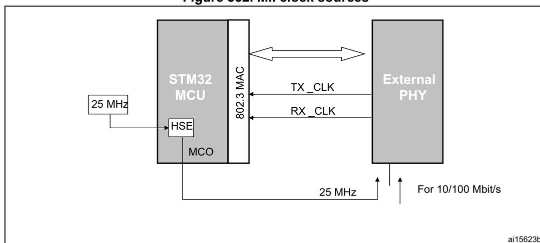
The diagram illustrates the clocking configuration for the MII interface. On the left, an STM32 MCU block contains an HSE (High-Speed External) input connected to a 25 MHz source and an MCO (Microcontroller Clock Output) pin. The MCO pin is connected to the TX_CLK and RX_CLK pins of an External PHY block on the right. The External PHY is labeled 'For 10/100 Mbit/s'. Between the HSE and the PHY, the 802.3 MAC block is shown. The diagram also includes a label 'ai15623b' in the bottom right corner.
29.4.3 Reduced media-independent interface: RMII
The reduced media-independent interface (RMII) specification reduces the pin count between the microcontroller Ethernet peripheral and the external Ethernet in 10/100 Mbit/s. According to the IEEE 802.3u standard, an MII contains 16 pins for data and control. The RMII specification is dedicated to reduce the pin count to 7 pins (a 62.5% decrease in pin count).
The RMII is instantiated between the MAC and the PHY. This helps translation of the MAC's MII into the RMII. The RMII block has the following characteristics:
- • It supports 10-Mbit/s and 100-Mbit/s operating rates
- • The clock reference must be doubled to 50 MHz
- • The same clock reference must be sourced externally to both MAC and external Ethernet PHY
- • It provides independent 2-bit wide (dibit) transmit and receive data paths
Figure 333. Reduced media-independent interface signals
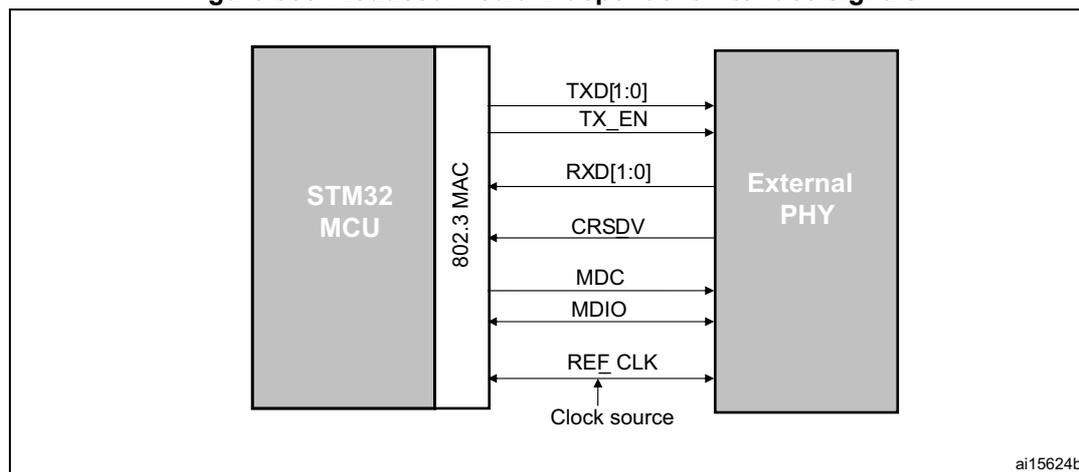
Diagram illustrating the Reduced media-independent interface (RMII) signals between an STM32 MCU and an External PHY. The STM32 MCU is connected to an 802.3 MAC block. The 802.3 MAC block is connected to the External PHY via the following signals: TXD[1:0], TX_EN, RXD[1:0], CRS_DV, MDC, MDIO, and REF_CLK. The REF_CLK signal is sourced from a Clock source. The diagram is labeled ai15624b.
RMII clock sources
As described in the RMII clock sources section, the STM32F10xxx/STM32F107xx could provide this 50 MHz clock signal on its MCO output pin and you then have to configure this output value through PLL configuration.
Figure 334. RMII clock sources
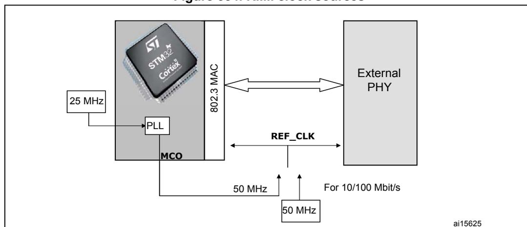
Diagram illustrating the RMII clock sources. A 25 MHz clock source is connected to a PLL block within the STM32 MCU. The PLL block outputs a 50 MHz clock signal to the MCO pin. The MCO pin is connected to the External PHY via the REF_CLK signal. The REF_CLK signal is also connected to a 50 MHz clock source. The diagram is labeled ai15625.
29.4.4 MII/RMII selection
The mode, MII or RMII, is selected using the configuration bit 23, MII_RMII_SEL, in the AFIO_MAPR register. The application has to set the MII/RMII mode while the Ethernet controller is under reset or before enabling the clocks.
MII/RMII internal clock scheme
The clock scheme required to support both the MII and RMII, as well as 10 and 100 Mbit/s operations is described in Figure 335 .
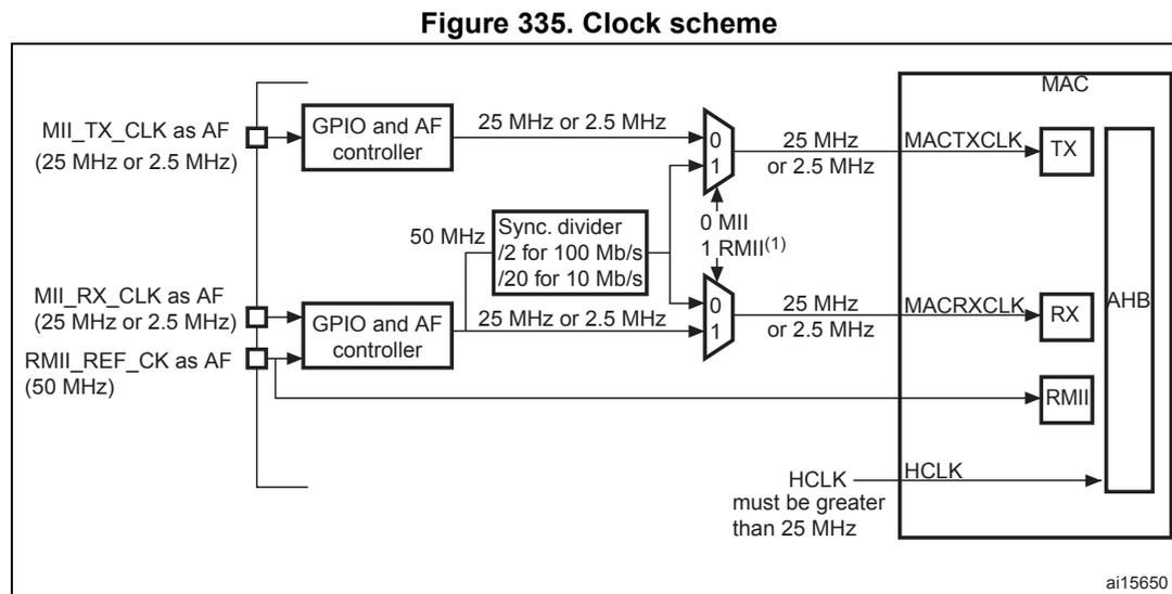
Figure 335. Clock scheme
The diagram illustrates the internal clock scheme for the Ethernet MAC. On the left, three input clock signals are shown:
- MII_TX_CLK as AF (25 MHz or 2.5 MHz)
- MII_RX_CLK as AF (25 MHz or 2.5 MHz)
- RMII_REF_CK as AF (50 MHz)
The MII_RX_CLK and RMII_REF_CK signals are also connected to a GPIO and AF controller . The MII_RX_CLK output (25 MHz or 2.5 MHz) is multiplexed (0 or 1) to provide the MAC_RX_CLK signal to the RX block. The RMII_REF_CK signal (50 MHz) is fed into a Sync. divider which has options for /2 for 100 Mb/s or /20 for 10 Mb/s . The output of this divider (25 MHz or 2.5 MHz) is also multiplexed (0 or 1) to provide the MAC_RX_CLK signal to the RX block.
A common HCLK signal is shown entering the MAC block from the bottom, with a note that HCLK must be greater than 25 MHz . The MAC block contains TX , RX , RMII , and AHB sub-blocks. The reference number ai15650 is located in the bottom right corner of the diagram.
- 1. The MII/RMII selection is controlled through bit 23, MII_RMII_SEL, in the AFIO_MAPR register.
To save a pin, the two input clock signals, RMII_REF_CK and MII_RX_CLK, are multiplexed on the same GPIO pin.
29.5 Ethernet functional description: MAC 802.3
The IEEE 802.3 International Standard for local area networks (LANs) employs the CSMA/CD (carrier sense multiple access with collision detection) as the access method.
The Ethernet peripheral consists of a MAC 802.3 (media access control) controller with media independent interface (MII) and a dedicated DMA controller.
The MAC block implements the LAN CSMA/CD sublayer for the following families of systems: 10 Mbit/s and 100 Mbit/s of data rates for baseband and broadband systems. Half- and full-duplex operation modes are supported. The collision detection access method is applied only to the half-duplex operation mode. The MAC control frame sublayer is supported.
The MAC sublayer performs the following functions associated with a data link control procedure:
- • Data encapsulation (transmit and receive)
- – Framing (frame boundary delimitation, frame synchronization)
- – Addressing (handling of source and destination addresses)
- – Error detection
- • Media access management
- – Medium allocation (collision avoidance)
- – Contention resolution (collision handling)
Basically there are two operating modes of the MAC sublayer:
- • Half-duplex mode: the stations contend for the use of the physical medium, using the CSMA/CD algorithms.
- • Full duplex mode: simultaneous transmission and reception without contention resolution (CSMA/CD algorithm are unnecessary) when all the following conditions are met:
- – physical medium capability to support simultaneous transmission and reception
- – exactly 2 stations connected to the LAN
- – both stations configured for full-duplex operation
29.5.1 MAC 802.3 frame format
The MAC block implements the MAC sublayer and the optional MAC control sublayer (10/100 Mbit/s) as specified by the IEEE 802.3-2002 standard.
Two frame formats are specified for data communication systems using the CSMA/CD MAC:
- • Basic MAC frame format
- • Tagged MAC frame format (extension of the basic MAC frame format)
Figure 337 and Figure 338 describe the frame structure (untagged and tagged) that includes the following fields:
- • Preamble: 7-byte field used for synchronization purposes (PLS circuitry)
Hexadecimal value: 55-55-55-55-55-55-55
Bit pattern: 01010101 01010101 01010101 01010101 01010101 01010101 01010101 (right-to-left bit transmission) - • Start frame delimiter (SFD): 1-byte field used to indicate the start of a frame.
Hexadecimal value: D5
Bit pattern: 11010101 (right-to-left bit transmission) - • Destination and Source Address fields: 6-byte fields to indicate the destination and source station addresses as follows (see
Figure 336
):
- – Each address is 48 bits in length
- – The first LSB bit (I/G) in the destination address field is used to indicate an individual (I/G = 0) or a group address (I/G = 1). A group address could identify
none, one or more, or all the stations connected to the LAN. In the source address the first bit is reserved and reset to 0.
- – The second bit (U/L) distinguishes between locally (U/L = 1) or globally (U/L = 0) administered addresses. For broadcast addresses this bit is also 1.
- – Each byte of each address field must be transmitted least significant bit first.
The address designation is based on the following types:
- • Individual address: this is the physical address associated with a particular station on the network.
- • Group address. A multdestination address associated with one or more stations on a given network. There are two kinds of multicast address:
- – Multicast-group address: an address associated with a group of logically related stations.
- – Broadcast address: a distinguished, predefined multicast address (all 1's in the destination address field) that always denotes all the stations on a given LAN.
Figure 336. Address field format
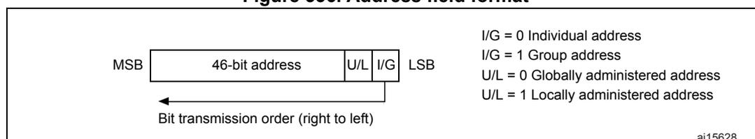
I/G = 0 Individual address
I/G = 1 Group address
U/L = 0 Globally administered address
U/L = 1 Locally administered address
ai15628
- • QTag Prefix: 4-byte field inserted between the Source address field and the MAC Client Length/Type field. This field is an extension of the basic frame (untagged) to obtain the tagged MAC frame. The untagged MAC frames do not include this field. The extensions for tagging are as follows:
- – 2-byte constant Length/Type field value consistent with the Type interpretation (greater than 0x0600) equal to the value of the 802.1Q Tag Protocol Type (0x8100 hexadecimal). This constant field is used to distinguish tagged and untagged MAC frames.
- – 2-byte field containing the Tag control information field subdivided as follows: a 3-bit user priority, a canonical format indicator (CFI) bit and a 12-bit VLAN Identifier. The length of the tagged MAC frame is extended by 4 bytes by the QTag Prefix.
- • MAC client length/type: 2-byte field with different meaning (mutually exclusive), depending on its value:
- – If the value is less than or equal to maxValidFrame (0d1500) then this field indicates the number of MAC client data bytes contained in the subsequent data field of the 802.3 frame (length interpretation).
- – If the value is greater than or equal to MinTypeValue (0d1536 decimal, 0x0600) then this field indicates the nature of the MAC client protocol (Type interpretation) related to the Ethernet frame.
Regardless of the interpretation of the length/type field, if the length of the data field is less than the minimum required for proper operation of the protocol, a PAD field is
added after the data field but prior to the FCS (frame check sequence) field. The length/type field is transmitted and received with the higher-order byte first.
For length/type field values in the range between maxValidLength and minTypeValue (boundaries excluded), the behavior of the MAC sublayer is not specified: they may or may not be passed by the MAC sublayer.
- • Data and PAD fields: n-byte data field. Full data transparency is provided, it means that any arbitrary sequence of byte values may appear in the data field. The size of the PAD, if any, is determined by the size of the data field. Max and min length of the data and PAD field are:
- – Maximum length = 1500 bytes
- – Minimum length for untagged MAC frames = 46 bytes
- – Minimum length for tagged MAC frames = 42 bytes
When the data field length is less than the minimum required, the PAD field is added to match the minimum length (42 bytes for tagged frames, 46 bytes for untagged frames).
- • Frame check sequence: 4-byte field that contains the cyclic redundancy check (CRC) value. The CRC computation is based on the following fields: source address, destination address, QTag prefix, length/type, LLC data and PAD (that is, all fields except the preamble, SFD). The generating polynomial is the following:
The CRC value of a frame is computed as follows:
- • The first 2 bits of the frame are complemented
- • The n-bits of the frame are the coefficients of a polynomial \( M(x) \) of degree \( (n - 1) \) . The first bit of the destination address corresponds to the \( x^{n-1} \) term and the last bit of the data field corresponds to the \( x^0 \) term
- • \( M(x) \) is multiplied by \( x^{32} \) and divided by \( G(x) \) , producing a remainder \( R(x) \) of degree \( \leq 31 \)
- • The coefficients of \( R(x) \) are considered as a 32-bit sequence
- • The bit sequence is complemented and the result is the CRC
- • The 32-bits of the CRC value are placed in the frame check sequence. The \( x^{32} \) term is the first transmitted, the \( x^0 \) term is the last one
Figure 337. MAC frame format
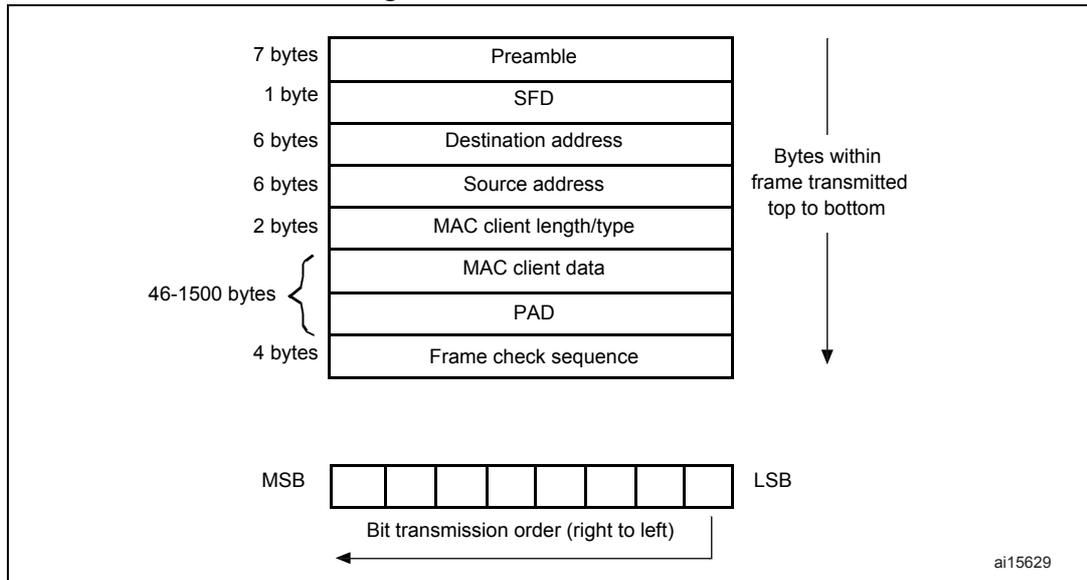
The diagram shows the structure of a standard MAC frame. The fields are listed from top to bottom: Preamble (7 bytes), SFD (1 byte), Destination address (6 bytes), Source address (6 bytes), MAC client length/type (2 bytes), MAC client data (46-1500 bytes), PAD (part of the data), and Frame check sequence (4 bytes). A bracket on the left groups the MAC client data and PAD fields. To the right, a vertical arrow indicates that bytes within the frame are transmitted from top to bottom. Below the frame structure, a bit transmission order diagram shows a byte with MSB on the left and LSB on the right, with an arrow indicating transmission from right to left. The identifier 'ai15629' is in the bottom right corner.
Figure 338. Tagged MAC frame format
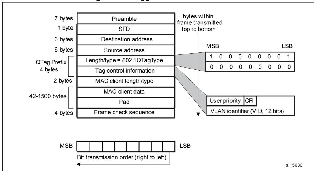
This diagram shows the structure of a tagged MAC frame. It is similar to the standard frame but includes a 4-byte QTag Prefix inserted after the Source address. The QTag Prefix consists of a Length/type field set to 802.1QTagType and a Tag control information field. A callout box provides a detailed view of the Tag control information, showing 16 bits: the first bit is User priority, the second is CFI, and the remaining 14 bits are the VLAN identifier (VID, 12 bits). The bit transmission order diagram at the bottom is identical to Figure 337. The identifier 'ai15630' is in the bottom right corner.
Each byte of the MAC frame, except the FCS field, is transmitted low-order bit first.
An invalid MAC frame is defined by one of the following conditions:
- • The frame length is inconsistent with the expected value as specified by the length/type field. If the length/type field contains a type value, then the frame length is assumed to be consistent with this field (no invalid frame)
- • The frame length is not an integer number of bytes (extra bits)
- • The CRC value computed on the incoming frame does not match the included FCS
29.5.2 MAC frame transmission
The DMA controls all transactions for the transmit path. Ethernet frames read from the system memory are pushed into the FIFO by the DMA. The frames are then popped out and transferred to the MAC core. When the end-of-frame is transferred, the status of the transmission is taken from the MAC core and transferred back to the DMA. The Transmit FIFO has a depth of 2 Kbyte. FIFO-fill level is indicated to the DMA so that it can initiate a data fetch in required bursts from the system memory, using the AHB interface. The data from the AHB Master interface is pushed into the FIFO.
When the SOF is detected, the MAC accepts the data and begins transmitting to the MII. The time required to transmit the frame data to the MII after the application initiates transmission is variable, depending on delay factors like IFG delay, time to transmit preamble/SFD, and any back-off delays for Half-duplex mode. After the EOF is transferred to the MAC core, the core completes normal transmission and then gives the status of transmission back to the DMA. If a normal collision (in Half-duplex mode) occurs during transmission, the MAC core makes the transmit status valid, then accepts and drops all further data until the next SOF is received. The same frame should be retransmitted from SOF on observing a Retry request (in the Status) from the MAC. The MAC issues an underflow status if the data are not provided continuously during the transmission. During the normal transfer of a frame, if the MAC receives an SOF without getting an EOF for the previous frame, then the SOF is ignored and the new frame is considered as the continuation of the previous frame.
There are two modes of operation for popping data towards the MAC core:
- • In Threshold mode, as soon as the number of bytes in the FIFO crosses the configured threshold level (or when the end-of-frame is written before the threshold is crossed), the data is ready to be popped out and forwarded to the MAC core. The threshold level is configured using the TTC bits of ETH_DMAABMR.
- • In Store-and-forward mode, only after a complete frame is stored in the FIFO, the frame is popped towards the MAC core. If the Tx FIFO size is smaller than the Ethernet frame to be transmitted, then the frame is popped towards the MAC core when the Tx FIFO becomes almost full.
The application can flush the Transmit FIFO of all contents by setting the FTF (ETH_DMAOMR register [20]) bit. This bit is self-clearing and initializes the FIFO pointers to the default state. If the FTF bit is set during a frame transfer to the MAC core, then transfer is stopped as the FIFO is considered to be empty. Hence an underflow event occurs at the MAC transmitter and the corresponding Status word is forwarded to the DMA.
Automatic CRC and pad generation
When the number of bytes received from the application falls below 60 (DA+SA+LT+Data), zeros are appended to the transmitting frame to make the data length exactly 46 bytes to meet the minimum data field requirement of IEEE 802.3. The MAC can be programmed not to append any padding. The cyclic redundancy check (CRC) for the frame check sequence (FCS) field is calculated and appended to the data being transmitted. When the MAC is programmed to not append the CRC value to the end of Ethernet frames, the computed CRC is not transmitted. An exception to this rule is that when the MAC is programmed to append pads for frames (DA+SA+LT+Data) less than 60 bytes, CRC will be appended at the end of the padded frames.
The CRC generator calculates the 32-bit CRC for the FCS field of the Ethernet frame. The encoding is defined by the following polynomial.
Transmit protocol
The MAC controls the operation of Ethernet frame transmission. It performs the following functions to meet the IEEE 802.3/802.3z specifications. It:
- • generates the preamble and SFD
- • generates the jam pattern in Half-duplex mode
- • controls the Jabber timeout
- • controls the flow for Half-duplex mode (back pressure)
- • generates the transmit frame status
- • contains time stamp snapshot logic in accordance with IEEE 1588
When a new frame transmission is requested, the MAC sends out the preamble and SFD, followed by the data. The preamble is defined as 7 bytes of 0b10101010 pattern, and the SFD is defined as 1 byte of 0b10101011 pattern. The collision window is defined as 1 slot time (512 bit times for 10/100 Mbit/s Ethernet). The jam pattern generation is applicable only to Half-duplex mode, not to Full-duplex mode.
In MII mode, if a collision occurs at any time from the beginning of the frame to the end of the CRC field, the MAC sends a 32-bit jam pattern of 0x5555 5555 on the MII to inform all other stations that a collision has occurred. If the collision is seen during the preamble transmission phase, the MAC completes the transmission of the preamble and SFD and then sends the jam pattern.
A jabber timer is maintained to cut off the transmission of Ethernet frames if more than 2048 (default) bytes have to be transferred. The MAC uses the deferral mechanism for flow control (back pressure) in Half-duplex mode. When the application requests to stop receiving frames, the MAC sends a JAM pattern of 32 bytes whenever it senses the reception of a frame, provided that transmit flow control is enabled. This results in a collision and the remote station backs off. The application requests flow control by setting the BPA bit (bit 0) in the ETH_MACFCR register. If the application requests a frame to be transmitted, then it is scheduled and transmitted even when back pressure is activated. Note that if back pressure is kept activated for a long time (and more than 16 consecutive collision events occur) then the remote stations abort their transmissions due to excessive collisions. If IEEE 1588 time stamping is enabled for the transmit frame, this block takes a snapshot of the system time when the SFD is put onto the transmit MII bus.
Transmit scheduler
The MAC is responsible for scheduling the frame transmission on the MII. It maintains the interframe gap between two transmitted frames and follows the truncated binary exponential backoff algorithm for Half-duplex mode. The MAC enables transmission after satisfying the IFG and backoff delays. It maintains an idle period of the configured interframe gap (IFG bits in the ETH_MACCR register) between any two transmitted frames. If frames to be transmitted arrive sooner than the configured IFG time, the MII waits for the enable signal from the MAC before starting the transmission on it. The MAC starts its IFG counter as soon as the carrier signal of the MII goes inactive. At the end of the programmed IFG value, the MAC enables transmission in Full-duplex mode. In Half-duplex mode and when IFG is
configured for 96 bit times, the MAC follows the rule of deference specified in Section 4.2.3.2.1 of the IEEE 802.3 specification. The MAC resets its IFG counter if a carrier is detected during the first two-thirds (64-bit times for all IFG values) of the IFG interval. If the carrier is detected during the final one third of the IFG interval, the MAC continues the IFG count and enables the transmitter after the IFG interval. The MAC implements the truncated binary exponential backoff algorithm when it operates in Half-duplex mode.
Transmit flow control
When the Transmit Flow Control Enable bit (TFE bit in ETH_MACFCR) is set, the MAC generates Pause frames and transmits them as necessary, in Full-duplex mode. The Pause frame is appended with the calculated CRC, and is sent. Pause frame generation can be initiated in two ways.
A pause frame is sent either when the application sets the FCB bit in the ETH_MACFCR register or when the receive FIFO is full (packet buffer).
- • If the application has requested flow control by setting the FCB bit in ETH_MACFCR, the MAC generates and transmits a single Pause frame. The value of the pause time in the generated frame contains the programmed pause time value in ETH_MACFCR. To extend the pause or end the pause prior to the time specified in the previously transmitted Pause frame, the application must request another Pause frame transmission after programming the Pause Time value (PT in ETH_MACFCR register) with the appropriate value.
- • If the application has requested flow control when the receive FIFO is full, the MAC generates and transmits a Pause frame. The value of the pause time in the generated frame is the programmed pause time value in ETH_MACFCR. If the receive FIFO remains full at a configurable number of slot-times (PLT bits in ETH_MACFCR) before this Pause time runs out, a second Pause frame is transmitted. The process is repeated as long as the receive FIFO remains full. If this condition is no more satisfied prior to the sampling time, the MAC transmits a Pause frame with zero pause time to indicate to the remote end that the receive buffer is ready to receive new data frames.
Single-packet transmit operation
The general sequence of events for a transmit operation is as follows:
- 1. If the system has data to be transferred, the DMA controller fetches them from the memory through the AHB Master interface and starts forwarding them to the FIFO. It continues to receive the data until the end of frame is transferred.
- 2. When the threshold level is crossed or a full packet of data is received into the FIFO, the frame data are popped and driven to the MAC core. The DMA continues to transfer data from the FIFO until a complete packet has been transferred to the MAC. Upon completion of the frame, the DMA controller is notified by the status coming from the MAC.
Transmit operation—Two packets in the buffer
- 1. Because the DMA must update the descriptor status before releasing it to the Host, there can be at the most two frames inside a transmit FIFO. The second frame is fetched by the DMA and put into the FIFO only if the OSF (operate on second frame) bit is set. If this bit is not set, the next frame is fetched from the memory only after the MAC has completely processed the frame and the DMA has released the descriptors.
- 2. If the OSF bit is set, the DMA starts fetching the second frame immediately after completing the transfer of the first frame to the FIFO. It does not wait for the status to be updated. In the meantime, the second frame is received into the FIFO while the first
frame is being transmitted. As soon as the first frame has been transferred and the status is received from the MAC, it is pushed to the DMA. If the DMA has already completed sending the second packet to the FIFO, the second transmission must wait for the status of the first packet before proceeding to the next frame.
Retransmission during collision
While a frame is being transferred to the MAC, a collision event may occur on the MAC line interface in Half-duplex mode. The MAC would then indicate a retry attempt by giving the status even before the end of frame is received. Then the retransmission is enabled and the frame is popped out again from the FIFO. After more than 96 bytes have been popped towards the MAC core, the FIFO controller frees up that space and makes it available to the DMA to push in more data. This means that the retransmission is not possible after this threshold is crossed or when the MAC core indicates a late collision event.
Transmit FIFO flush operation
The MAC provides a control to the software to flush the Transmit FIFO through the use of Bit 20 in the Operation mode register. The Flush operation is immediate and the Tx FIFO and the corresponding pointers are cleared to the initial state even if the Tx FIFO is in the middle of transferring a frame to the MAC Core. This results in an underflow event in the MAC transmitter, and the frame transmission is aborted. The status of such a frame is marked with both underflow and frame flush events (TDES0 bits 13 and 1). No data are coming to the FIFO from the application (DMA) during the Flush operation. Transfer transmit status words are transferred to the application for the number of frames that is flushed (including partial frames). Frames that are completely flushed have the Frame flush status bit (TDES0 13) set. The Flush operation is completed when the application (DMA) has accepted all of the Status words for the frames that were flushed. The Transmit FIFO Flush control register bit is then cleared. At this point, new frames from the application (DMA) are accepted. All data presented for transmission after a Flush operation are discarded unless they start with an SOF marker.
Transmit status word
At the end of the Ethernet frame transfer to the MAC core and after the core has completed the transmission of the frame, the transmit status is given to the application. The detailed description of the Transmit Status is the same as for bits [23:0] in TDES0. If IEEE 1588 time stamping is enabled, a specific frames' 64-bit time stamp is returned, along with the transmit status.
Transmit checksum offload
Communication protocols such as TCP and UDP implement checksum fields, which helps determine the integrity of data transmitted over a network. Because the most widespread use of Ethernet is to encapsulate TCP and UDP over IP datagrams, the Ethernet controller has a transmit checksum offload feature that supports checksum calculation and insertion in the transmit path, and error detection in the receive path. This section explains the operation of the checksum offload feature for transmitted frames.
Note: The checksum for TCP, UDP or ICMP is calculated over a complete frame, then inserted into its corresponding header field. Due to this requirement, this function is enabled only when the Transmit FIFO is configured for Store-and-forward mode (that is, when the TSF bit
is set in the ETH_ETH_DMAOMR register). If the core is configured for Threshold (cut-through) mode, the Transmit checksum offload is bypassed.
You must make sure the Transmit FIFO is deep enough to store a complete frame before that frame is transferred to the MAC Core transmitter. If the FIFO depth is less than the input Ethernet frame size, the payload (TCP/UDP/ICMP) checksum insertion function is bypassed and only the frame's IPv4 Header checksum is modified, even in Store-and-forward mode.
The transmit checksum offload supports two types of checksum calculation and insertion. This checksum can be controlled for each frame by setting the CIC bits (Bits 28:27 in TDES1, described in TDES1: Transmit descriptor Word1 ).
See IETF specifications RFC 791, RFC 793, RFC 768, RFC 792, RFC 2460 and RFC 4443 for IPv4, TCP, UDP, ICMP, IPv6 and ICMPv6 packet header specifications, respectively.
- • IP header checksum
In IPv4 datagrams, the integrity of the header fields is indicated by the 16-bit header checksum field (the eleventh and twelfth bytes of the IPv4 datagram). The checksum offload detects an IPv4 datagram when the Ethernet frame's Type field has the value 0x0800 and the IP datagram's Version field has the value 0x4. The input frame's checksum field is ignored during calculation and replaced by the calculated value. IPv6 headers do not have a checksum field; thus, the checksum offload does not modify IPv6 header fields. The result of this IP header checksum calculation is indicated by the IP Header Error status bit in the Transmit status (Bit 16). This status bit is set whenever the values of the Ethernet Type field and the IP header's Version field are not consistent, or when the Ethernet frame does not have enough data, as indicated by the IP header Length field. In other words, this bit is set when an IP header error is asserted under the following circumstances:
- For IPv4 datagrams:
- – The received Ethernet type is 0x0800, but the IP header's Version field does not equal 0x4
- – The IPv4 Header Length field indicates a value less than 0x5 (20 bytes)
- – The total frame length is less than the value given in the IPv4 Header Length field
- For IPv6 datagrams:
- – The Ethernet type is 0x86DD but the IP header Version field does not equal 0x6
- – The frame ends before the IPv6 header (40 bytes) or extension header (as given in the corresponding Header Length field in an extension header) has been completely received. Even when the checksum offload detects such an IP header
error, it inserts an IPv4 header checksum if the Ethernet Type field indicates an IPv4 payload.
- • TCP/UDP/ICMP checksum
The TCP/UDP/ICMP checksum processes the IPv4 or IPv6 header (including extension headers) and determines whether the encapsulated payload is TCP, UDP or ICMP.
Note that:
- a) For non-TCP, -UDP, or -ICMP/ICMPv6 payloads, this checksum is bypassed and nothing further is modified in the frame.
- b) Fragmented IP frames (IPv4 or IPv6), IP frames with security features (such as an authentication header or encapsulated security payload), and IPv6 frames with routing headers are bypassed and not processed by the checksum.
The checksum is calculated for the TCP, UDP, or ICMP payload and inserted into its corresponding field in the header. It can work in the following two modes:
- – In the first mode, the TCP, UDP, or ICMPv6 pseudo-header is not included in the checksum calculation and is assumed to be present in the input frame's checksum field. The checksum field is included in the checksum calculation, and then replaced by the final calculated checksum.
- – In the second mode, the checksum field is ignored, the TCP, UDP, or ICMPv6 pseudo-header data are included into the checksum calculation, and the checksum field is overwritten with the final calculated value.
Note that: for ICMP-over-IPv4 packets, the checksum field in the ICMP packet must always be 0x0000 in both modes, because pseudo-headers are not defined for such packets. If it does not equal 0x0000, an incorrect checksum may be inserted into the packet.
The result of this operation is indicated by the payload checksum error status bit in the Transmit Status vector (bit 12). The payload checksum error status bit is set when either of the following is detected:
- – the frame has been forwarded to the MAC transmitter in Store-and-forward mode without the end of frame being written to the FIFO
- – the packet ends before the number of bytes indicated by the payload length field in the IP header is received.
When the packet is longer than the indicated payload length, the bytes are ignored as stuff bytes, and no error is reported. When the first type of error is detected, the TCP, UDP or ICMP header is not modified. For the second error type, still, the calculated checksum is inserted into the corresponding header field.
MII/RMII transmit bit order
Each nibble from the MII is transmitted on the RMII a dibit at a time with the order of dibit transmission shown in Figure 339 . Lower order bits (D1 and D0) are transmitted first followed by higher order bits (D2 and D3).
Figure 339. Transmission bit order
![Diagram showing the transmission bit order for a nibble stream. A nibble stream (D0, D1, D2, D3) is shown with LSB at the top and MSB at the bottom. The nibble stream is converted into a bit stream (D0, D1) with LSB at the top and MSB at the bottom. The conversion is labeled RMII_TXD[1:0].](/RM0008-STM32F101-102-103-105-107/ffa781d7856e6f4108ab9b2c31c37d85_img.jpg)
The diagram illustrates the bit order for transmission. On the left, a 'Nibble stream' is shown as a vertical stack of four cells labeled D0, D1, D2, and D3. Above D0 is the label 'LSB' and below D3 is 'MSB'. An arrow labeled 'MII_TXD[3:0]' points to this stack. On the right, a 'Bit stream' is shown as a vertical stack of two cells labeled D0 and D1. Above D0 is 'LSB' and above D1 is 'MSB'. An arrow labeled 'RMII_TXD[1:0]' points to this stack. Dashed lines connect D0 to D0 and D1 to D1. Solid lines connect D2 to D0 and D3 to D1. The text 'ai15632' is in the bottom right corner.
MII/RMII transmit timing diagrams
Figure 340. Transmission with no collision
![Timing diagram for transmission with no collision. It shows five signals over time: MII_TX_CLK (clock), MII_TX_EN (enable), MII_TXD[3:0] (data), MII_CS (carrier sense), and MII_COL (collision). The data signal shows a sequence of frames: PR, EA, MB, LE, followed by a gap, then another frame. The carrier sense signal is high during transmission. The collision signal is low throughout the shown period.](/RM0008-STM32F101-102-103-105-107/194fa9f888b41872f275a6763a59e7c0_img.jpg)
The timing diagram shows five signals over time.
1.
MII_TX_CLK
: A periodic square wave clock signal.
2.
MII_TX_EN
: An active-low signal that goes low to start transmission and returns high to stop.
3.
MII_TXD[3:0]
: A 4-bit data bus. It shows a sequence of frames: PR (Preamble), EA (Destination MAC), MB (Source MAC), LE (Length/Type), followed by a gap (grey), then another frame.
4.
MII_CS
: Carrier Sense signal, which goes high when the transmitter is active and returns low when idle.
5.
MII_COL
: Collision signal, which is shown as 'Low' throughout the diagram.
Vertical dashed lines indicate clock edges. The text 'ai15631' is in the bottom right corner.
Figure 341. Transmission with collision
![Timing diagram for Figure 341: Transmission with collision. It shows five signals over time: MII_TX_CLK (a square wave clock), MII_TX_EN (transmit enable, goes high before data), MII_TXD[3:0] (4-bit data bus with fields PR, EAM, BLE, SFD, DA, DA, JAM, JAM, JAM, JAM), MII_CS (carrier sense, goes high when TX_EN is high), and MII_COL (collision, goes high during the collision period). The collision occurs during the transmission of the data fields.](/RM0008-STM32F101-102-103-105-107/c5a8b0ac7f90e800533355de63ecba19_img.jpg)
Figure 342 shows a frame transmission in MII and RMII.
Figure 342. Frame transmission in MMI and RMII modes
![Timing diagram for Figure 342: Frame transmission in MMI and RMII modes. It compares MII and RMII signals. MII_RX_CLK is a receive clock. MII_TX_EN is the MII transmit enable. MII_TXD[3:0] shows the MII data bus. RMII_REF_CLK is a reference clock for RMII. RMII_TX_EN is the RMII transmit enable. RMII_TXD[1:0] shows the RMII data bus. The diagram illustrates the timing relationship between the various signals during a frame transmission in both modes.](/RM0008-STM32F101-102-103-105-107/b7b3364adb40fc4805e27463dc74101a_img.jpg)
29.5.3 MAC frame reception
The MAC received frames are pushed into the Rx FIFO. The status (fill level) of this FIFO is indicated to the DMA once it crosses the configured receive threshold (RTC in the ETH_DMAOMR register) so that the DMA can initiate pre-configured burst transfers towards the AHB interface.
In the default Cut-through mode, when 64 bytes (configured with the RTC bits in the ETH_DMAOMR register) or a full packet of data are received into the FIFO, the data are popped out and the DMA is notified of its availability. Once the DMA has initiated the transfer to the AHB interface, the data transfer continues from the FIFO until a complete
packet has been transferred. Upon completion of the EOF frame transfer, the status word is popped out and sent to the DMA controller.
In Rx FIFO Store-and-forward mode (configured by the RSF bit in the ETH_DMAOMR register), a frame is read only after being written completely into the Receive FIFO. In this mode, all error frames are dropped (if the core is configured to do so) such that only valid frames are read and forwarded to the application. In Cut-through mode, some error frames are not dropped, because the error status is received at the end of the frame, by which time the start of that frame has already been read of the FIFO.
A receive operation is initiated when the MAC detects an SFD on the MII. The core strips the preamble and SFD before proceeding to process the frame. The header fields are checked for the filtering and the FCS field used to verify the CRC for the frame. The frame is dropped in the core if it fails the address filter.
Receive protocol
The received frame preamble and SFD are stripped. Once the SFD has been detected, the MAC starts sending the Ethernet frame data to the receive FIFO, beginning with the first byte following the SFD (destination address). If IEEE 1588 time stamping is enabled, a snapshot of the system time is taken when any frame's SFD is detected on the MII. Unless the MAC filters out and drops the frame, this time stamp is passed on to the application.
If the received frame length/type field is less than 0x600 and if the MAC is programmed for the auto CRC/pad stripping option, the MAC sends the data of the frame to RxFIFO up to the count specified in the length/type field, then starts dropping bytes (including the FCS field). If the Length/Type field is greater than or equal to 0x600, the MAC sends all received Ethernet frame data to Rx FIFO, regardless of the value on the programmed auto-CRC strip option. The MAC watchdog timer is enabled by default, that is, frames above 2048 bytes (DA + SA + LT + Data + pad + FCS) are cut off. This feature can be disabled by programming the watchdog disable (WD) bit in the MAC configuration register. However, even if the watchdog timer is disabled, frames greater than 16 KB in size are cut off and a watchdog timeout status is given.
Receive CRC: automatic CRC and pad stripping
The MAC checks for any CRC error in the receiving frame. It calculates the 32-bit CRC for the received frame that includes the Destination address field through the FCS field. The encoding is defined by the following polynomial.
Regardless of the auto-pad/CRC strip, the MAC receives the entire frame to compute the CRC check for the received frame.
Receive checksum offload
Both IPv4 and IPv6 frames in the received Ethernet frames are detected and processed for data integrity. You can enable the receive checksum offload by setting the IPCO bit in the ETH_MACCR register. The MAC receiver identifies IPv4 or IPv6 frames by checking for value 0x0800 or 0x86DD, respectively, in the received Ethernet frame Type field. This identification applies to VLAN-tagged frames as well. The receive checksum offload calculates IPv4 header checksums and checks that they match the received IPv4 header checksums. The IP Header Error bit is set for any mismatch between the indicated payload
type (Ethernet Type field) and the IP header version, or when the received frame does not have enough bytes, as indicated by the IPv4 header's Length field (or when fewer than 20 bytes are available in an IPv4 or IPv6 header). The receive checksum offload also identifies a TCP, UDP or ICMP payload in the received IP datagrams (IPv4 or IPv6) and calculates the checksum of such payloads properly, as defined in the TCP, UDP or ICMP specifications. It includes the TCP/UDP/ICMPv6 pseudo-header bytes for checksum calculation and checks whether the received checksum field matches the calculated value. The result of this operation is given as a Payload Checksum Error bit in the receive status word. This status bit is also set if the length of the TCP, UDP or ICMP payload does not match the expected payload length given in the IP header. As mentioned in TCP/UDP/ICMP checksum , the receive checksum offload bypasses the payload of fragmented IP datagrams, IP datagrams with security features, IPv6 routing headers, and payloads other than TCP, UDP or ICMP. This information (whether the checksum is bypassed or not) is given in the receive status, as described in the RDES0: Receive descriptor Word0 section. In this configuration, the core does not append any payload checksum bytes to the received Ethernet frames.
As mentioned in RDES0: Receive descriptor Word0 , the meaning of certain register bits changes as shown in Table 214 .
Table 214. Frame statuses
| Bit 18: Ethernet frame | Bit 27: Header checksum error | Bit 28: Payload checksum error | Frame status |
|---|---|---|---|
| 0 | 0 | 0 | The frame is an IEEE 802.3 frame (Length field value is less than 0x0600). |
| 1 | 0 | 0 | IPv4/IPv6 Type frame in which no checksum error is detected. |
| 1 | 0 | 1 | IPv4/IPv6 Type frame in which a payload checksum error (as described for PCE) is detected |
| 1 | 1 | 0 | IPv4/IPv6 Type frame in which IP header checksum error (as described for IPCO HCE) is detected. |
| 1 | 1 | 1 | IPv4/IPv6 Type frame in which both PCE and IPCO HCE are detected. |
| 0 | 0 | 1 | IPv4/IPv6 Type frame in which there is no IP HCE and the payload check is bypassed due to unsupported payload. |
| 0 | 1 | 1 | Type frame which is neither IPv4 or IPv6 (checksum offload bypasses the checksum check completely) |
| 0 | 1 | 0 | Reserved |
Receive frame controller
If the RA bit is reset in the MAC CSR frame filter register, the MAC performs frame filtering based on the destination/source address (the application still needs to perform another level of filtering if it decides not to receive any bad frames like runt, CRC error frames, etc.). On detecting a filter-fail, the frame is dropped and not transferred to the application. When the filtering parameters are changed dynamically, and in case of (DA-SA) filter-fail, the rest of the frame is dropped and the Rx Status Word is immediately updated (with zero frame
length, CRC error and Runt Error bits set), indicating the filter fail. In Ethernet power down mode, all received frames are dropped, and are not forwarded to the application.
Receive flow control
The MAC detects the receiving Pause frame and pauses the frame transmission for the delay specified within the received Pause frame (only in Full-duplex mode). The Pause frame detection function can be enabled or disabled with the RFCE bit in ETH_MACFCR. Once receive flow control has been enabled, the received frame destination address begins to be monitored for any match with the multicast address of the control frame (0x0180 C200 0001). If a match is detected (the destination address of the received frame matches the reserved control frame destination address), the MAC then decides whether or not to transfer the received control frame to the application, based on the level of the PCF bit in ETH_MACFFR.
The MAC also decodes the type, opcode, and Pause Timer fields of the receiving control frame. If the byte count of the status indicates 64 bytes, and if there is no CRC error, the MAC transmitter pauses the transmission of any data frame for the duration of the decoded Pause time value, multiplied by the slot time (64 byte times for both 10/100 Mbit/s modes). Meanwhile, if another Pause frame is detected with a zero Pause time value, the MAC resets the Pause time and manages this new pause request.
If the received control frame matches neither the type field (0x8808), the opcode (0x00001), nor the byte length (64 bytes), or if there is a CRC error, the MAC does not generate a Pause.
In the case of a pause frame with a multicast destination address, the MAC filters the frame based on the address match.
For a pause frame with a unicast destination address, the MAC filtering depends on whether the DA matched the contents of the MAC address 0 register and whether the UPDF bit in ETH_MACFCR is set (detecting a pause frame even with a unicast destination address). The PCF register bits (bits [7:6] in ETH_MACFFR) control filtering for control frames in addition to address filtering.
Receive operation multiframe handling
Since the status is available immediately following the data, the FIFO is capable of storing any number of frames into it, as long as it is not full.
Error handling
If the Rx FIFO is full before it receives the EOF data from the MAC, an overflow is declared and the whole frame is dropped, and the overflow counter in the (ETH_DMAMFBOCR register) is incremented. The status indicates a partial frame due to overflow. The Rx FIFO can filter error and undersized frames, if enabled (using the FEF and FUGF bits in ETH_DMAOMR).
If the Receive FIFO is configured to operate in Store-and-forward mode, all error frames can be filtered and dropped.
In Cut-through mode, if a frame's status and length are available when that frame's SOF is read from the Rx FIFO, then the complete erroneous frame can be dropped. The DMA can flush the error frame being read from the FIFO, by enabling the receive frame flash bit. The data transfer to the application (DMA) is then stopped and the rest of the frame is internally read and dropped. The next frame transfer can then be started, if available.
Receive status word
At the end of the Ethernet frame reception, the MAC outputs the receive status to the application (DMA). The detailed description of the receive status is the same as for bits[31:0] in RDES0, given in RDES0: Receive descriptor Word0 .
Frame length interface
In case of switch applications, data transmission and reception between the application and MAC happen as complete frame transfers. The application layer should be aware of the length of the frames received from the ingress port in order to transfer the frame to the egress port. The MAC core provides the frame length of each received frame inside the status at the end of each frame reception.
Note: A frame length value of 0 is given for partial frames written into the Rx FIFO due to overflow.
MII/RMII receive bit order
Each nibble is transmitted to the MII from the dibit received from the RMII in the nibble transmission order shown in Figure 343 . The lower-order bits (D0 and D1) are received first, followed by the higher-order bits (D2 and D3).
Figure 343. Receive bit order
![Diagram illustrating the receive bit order for MII/RMII. A vertical stack of four bits (D0, D1, D2, D3) represents the nibble stream, with D0 at the top (LSB) and D3 at the bottom (MSB). An arrow labeled 'MII_RXD[3:0]' points to this stack. Above the stack, a horizontal box contains two bits, D0 and D1, labeled 'Di-bit stream'. Above this box, an arrow labeled 'RMII_RXD[1:0]' points upwards, with 'LSB' on the left and 'MSB' on the right. Dashed lines connect D0 and D1 from the Di-bit stream to the corresponding positions in the nibble stream. The diagram is labeled 'ai15633' in the bottom right corner.](/RM0008-STM32F101-102-103-105-107/e267c4cdd8baf989ff95307501353401_img.jpg)
The diagram illustrates the receive bit order. On the left, a vertical stack of four bits labeled D0, D1, D2, and D3 represents the 'Nibble stream'. D0 is at the top, marked as 'LSB', and D3 is at the bottom, marked as 'MSB'. An arrow labeled 'MII_RXD[3:0]' points to this stack. Above the stack, a horizontal box contains two bits, D0 and D1, labeled 'Di-bit stream'. Above this box, an arrow labeled 'RMII_RXD[1:0]' points upwards, with 'LSB' on the left and 'MSB' on the right. Dashed lines connect D0 and D1 from the Di-bit stream to the corresponding positions in the nibble stream. The diagram is labeled 'ai15633' in the bottom right corner.
Figure 344. Reception with no error
![Timing diagram for Figure 344 showing successful Ethernet reception. The diagram includes four signals: MII_RX_CLK (a continuous square wave), MII_RX_DV (Data Valid signal, high during data reception), MII_RXD[3:0] (4-bit data bus showing PREAMBLE, SFD, data, and FCS), and MII_RX_ERR (error signal, which remains low throughout the reception).](/RM0008-STM32F101-102-103-105-107/f8be66de0f709b251feb6132441c349a_img.jpg)
Figure 345. Reception with errors
![Timing diagram for Figure 345 showing Ethernet reception with errors. The signals are similar to Figure 344, but the MII_RXD[3:0] bus contains 'XX' (invalid) symbols after the SFD. The MII_RX_ERR signal goes high during the reception of these invalid symbols and returns low after the error sequence.](/RM0008-STM32F101-102-103-105-107/46d8c16b74a03c252995f0c42dbe9975_img.jpg)
Figure 346. Reception with false carrier indication
![Timing diagram for Figure 346 showing a false carrier indication. The MII_RX_DV signal is high, indicating a carrier, but the data on the MII_RXD[3:0] bus is mostly 'XX' (invalid), with one '0E' value. The MII_RX_ERR signal goes high when the invalid data is detected.](/RM0008-STM32F101-102-103-105-107/60ca052a759727014c0d408897f9aa70_img.jpg)
29.5.4 MAC interrupts
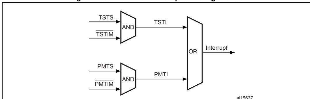
Interrupts can be generated from the MAC core as a result of various events.
The ETH_MACCSR register describes the events that can cause an interrupt from the MAC core. You can prevent each event from asserting the interrupt by setting the corresponding mask bits in the Interrupt Mask register.
The interrupt register bits only indicate the block from which the event is reported. You have to read the corresponding status registers and other registers to clear the interrupt. For example, bit 3 of the Interrupt register, set high, indicates that the Magic packet or Wake-on-LAN frame is received in Power-down mode. You must read the ETH_MACPMTCSR register to clear this interrupt event.
Figure 347. MAC core interrupt masking scheme
29.5.5 MAC filtering
Address filtering
Address filtering checks the destination and source addresses on all received frames and the address filtering status is reported accordingly. Address checking is based on different parameters (Frame filter register) chosen by the application. The filtered frame can also be identified: multicast or broadcast frame.
Address filtering uses the station's physical (MAC) address and the Multicast Hash table for address checking purposes.
Unicast destination address filter
The MAC supports up to 4 MAC addresses for unicast perfect filtering. If perfect filtering is selected (HU bit in the Frame filter register is reset), the MAC compares all 48 bits of the received unicast address with the programmed MAC address for any match. Default MacAddr0 is always enabled, other addresses MacAddr1–MacAddr3 are selected with an individual enable bit. Each byte of these other addresses (MacAddr1–MacAddr3) can be masked during comparison with the corresponding received DA byte by setting the corresponding Mask Byte Control bit in the register. This helps group address filtering for the DA. In Hash filtering mode (when HU bit is set), the MAC performs imperfect filtering for unicast addresses using a 64-bit Hash table. For hash filtering, the MAC uses the 6 upper CRC (see note 1 below) bits of the received destination address to index the content of the Hash table. A value of 000000 selects bit 0 in the selected register, and a value of 111111 selects bit 63 in the Hash Table register. If the corresponding bit (indicated by the 6-bit CRC) is set to 1, the unicast frame is said to have passed the Hash filter; otherwise, the frame has failed the Hash filter.
Note: This CRC is a 32-bit value coded by the following polynomial (for more details refer to Section 29.5.3):
Multicast destination address filter
The MAC can be programmed to pass all multicast frames by setting the PAM bit in the Frame filter register. If the PAM bit is reset, the MAC performs the filtering for multicast addresses based on the HM bit in the Frame filter register. In Perfect filtering mode, the multicast address is compared with the programmed MAC destination address registers (1–3). Group address filtering is also supported. In Hash filtering mode, the MAC performs imperfect filtering using a 64-bit Hash table. For hash filtering, the MAC uses the 6 upper CRC (see note 1 below) bits of the received multicast address to index the content of the Hash table. A value of 000000 selects bit 0 in the selected register and a value of 111111 selects bit 63 in the Hash Table register. If the corresponding bit is set to 1, then the multicast frame is said to have passed the Hash filter; otherwise, the frame has failed the Hash filter.
Note: This CRC is a 32-bit value coded by the following polynomial (for more details refer to Section 29.5.3 ):
Hash or perfect address filter
The DA filter can be configured to pass a frame when its DA matches either the Hash filter or the Perfect filter by setting the HPF bit in the Frame filter register and setting the corresponding HU or HM bits. This configuration applies to both unicast and multicast frames. If the HPF bit is reset, only one of the filters (Hash or Perfect) is applied to the received frame.
Broadcast address filter
The MAC does not filter any broadcast frames in the default mode. However, if the MAC is programmed to reject all broadcast frames by setting the BFD bit in the Frame filter register, any broadcast frames are dropped.
Unicast source address filter
The MAC can also perform perfect filtering based on the source address field of the received frames. By default, the MAC compares the SA field with the values programmed in the SA registers. The MAC address registers [1:3] can be configured to contain SA instead of DA for comparison, by setting bit 30 in the corresponding register. Group filtering with SA is also supported. The frames that fail the SA filter are dropped by the MAC if the SAF bit in the Frame filter register is set. Otherwise, the result of the SA filter is given as a status bit in the Receive Status word (see RDES0: Receive descriptor Word0 ).
When the SAF bit is set, the result of the SA and DA filters is AND'ed to decide whether the frame needs to be forwarded. This means that either of the filter fail result will drop the frame. Both filters have to pass the frame for the frame to be forwarded to the application.
Inverse filtering operation
For both destination and source address filtering, there is an option to invert the filter-match result at the final output. These are controlled by the DAIF and SAIF bits in the Frame filter register, respectively. The DAIF bit is applicable for both Unicast and Multicast DA frames. The result of the unicast/multicast destination address filter is inverted in this mode. Similarly, when the SAIF bit is set, the result of the unicast SA filter is inverted. Table 215
and Table 216 summarize destination and source address filtering based on the type of frame received.
Table 215. Destination address filtering
| Frame type | PM | HPF | HU | DAIF | HM | PAM | DB | DA filter operation |
|---|---|---|---|---|---|---|---|---|
| Broadcast | 1 | X | X | X | X | X | X | Pass |
| 0 | X | X | X | X | X | 0 | Pass | |
| 0 | X | X | X | X | X | 1 | Fail | |
| Unicast | 1 | X | X | X | X | X | X | Pass all frames |
| 0 | X | 0 | 0 | X | X | X | Pass on perfect/group filter match | |
| 0 | X | 0 | 1 | X | X | X | Fail on perfect/Group filter match | |
| 0 | 0 | 1 | 0 | X | X | X | Pass on hash filter match | |
| 0 | 0 | 1 | 1 | X | X | X | Fail on hash filter match | |
| 0 | 1 | 1 | 0 | X | X | X | Pass on hash or perfect/Group filter match | |
| 0 | 1 | 1 | 1 | X | X | X | Fail on hash or perfect/Group filter match | |
| Multicast | 1 | X | X | X | X | X | X | Pass all frames |
| X | X | X | X | X | 1 | X | Pass all frames | |
| 0 | X | X | 0 | 0 | 0 | X | Pass on Perfect/Group filter match and drop PAUSE control frames if PCF = 0x | |
| 0 | 0 | X | 0 | 1 | 0 | X | Pass on hash filter match and drop PAUSE control frames if PCF = 0x | |
| 0 | 1 | X | 0 | 1 | 0 | X | Pass on hash or perfect/Group filter match and drop PAUSE control frames if PCF = 0x | |
| 0 | X | X | 1 | 0 | 0 | X | Fail on perfect/Group filter match and drop PAUSE control frames if PCF = 0x | |
| 0 | 0 | X | 1 | 1 | 0 | X | Fail on hash filter match and drop PAUSE control frames if PCF = 0x | |
| 0 | 1 | X | 1 | 1 | 0 | X | Fail on hash or perfect/Group filter match and drop PAUSE control frames if PCF = 0x |
Table 216. Source address filtering
| Frame type | PM | SAIF | SAF | SA filter operation |
|---|---|---|---|---|
| Unicast | 1 | X | X | Pass all frames |
| 0 | 0 | 0 | Pass status on perfect/Group filter match but do not drop frames that fail | |
| 0 | 1 | 0 | Fail status on perfect/group filter match but do not drop frame | |
| 0 | 0 | 1 | Pass on perfect/group filter match and drop frames that fail | |
| 0 | 1 | 1 | Fail on perfect/group filter match and drop frames that fail |
29.5.6 MAC loopback mode
The MAC supports loopback of transmitted frames onto its receiver. By default, the MAC loopback function is disabled, but this feature can be enabled by programming the Loopback bit in the MAC ETH_MACCR register.
29.5.7 MAC management counters: MMC
The MAC management counters (MMC) maintain a set of registers for gathering statistics on the received and transmitted frames. These include a control register for controlling the behavior of the registers, two 32-bit registers containing generated interrupts (receive and transmit), and two 32-bit registers containing masks for the Interrupt register (receive and transmit). These registers are accessible from the application. Each register is 32 bits wide.
Section 29.8 describes the various counters and lists the addresses of each of the statistics counters. This address is used for read/write accesses to the desired transmit/receive counter.
The Receive MMC counters are updated for frames that pass address filtering. Dropped frames statistics are not updated unless the dropped frames are runt frames of less than 6 bytes (DA bytes are not received fully).
Good transmitted and received frames
Transmitted frames are considered “good” if transmitted successfully. In other words, a transmitted frame is good if the frame transmission is not aborted due to any of the following errors:
- + Jabber Timeout
- + No Carrier/Loss of Carrier
- + Late Collision
- + Frame Underflow
- + Excessive Deferral
- + Excessive Collision
Received frames are considered “good” if none of the following errors exists:
- + CRC error
- + Runt Frame (shorter than 64 bytes)
- + Alignment error (in 10/ 100 Mbit/s only)
- + Length error (non-Type frames only)
- + Out of Range (non-Type frames only, longer than maximum size)
- + MII_RXER Input error
The maximum frame size depends on the frame type, as follows:
- + Untagged frame maxsize = 1518
- + VLAN Frame maxsize = 1522
29.5.8 Power management: PMT
This section describes the power management (PMT) mechanisms supported by the MAC. PMT supports the reception of network (remote) wakeup frames and Magic Packet frames. PMT generates interrupts for wakeup frames and Magic Packets received by the MAC. The PMT block is enabled with remote wakeup frame enable and Magic Packet enable. These enable bits (WFE and MPE) are in the ETH_MACPMTCSR register and are programmed by the application. When the power down mode is enabled in the PMT, then all received frames are dropped by the MAC and they are not forwarded to the application. The MAC comes out of the power down mode only when either a Magic Packet or a Remote wakeup frame is received and the corresponding detection is enabled.
Remote wakeup frame filter register
There are eight wakeup frame filter registers. To write on each of them, load the wakeup frame filter register value by value. The wanted values of the wakeup frame filter are loaded by sequentially loading eight times the wakeup frame filter register. The read operation is identical to the write operation. To read the eight values, you have to read eight times the wakeup frame filter register to reach the last register. Each read/write points the wakeup frame filter register to the next filter register.
Figure 348. Wakeup frame filter register
| Wakeup frame filter reg0 | Filter 0 Byte Mask | |||||||
| Wakeup frame filter reg1 | Filter 1 Byte Mask | |||||||
| Wakeup frame filter reg2 | Filter 2 Byte Mask | |||||||
| Wakeup frame filter reg3 | Filter 3 Byte Mask | |||||||
| Wakeup frame filter reg4 | RSVD | Filter 3 Command | RSVD | Filter 2 Command | RSVD | Filter 1 Command | RSVD | Filter 0 Command |
| Wakeup frame filter reg5 | Filter 3 Offset | Filter 2 Offset | Filter 1 Offset | Filter 0 Offset | ||||
| Wakeup frame filter reg6 | Filter 1 CRC - 16 | Filter 0 CRC - 16 | ||||||
| Wakeup frame filter reg7 | Filter 3 CRC - 16 | Filter 2 CRC - 16 | ||||||
ai15647
- • Filter i Byte Mask
This register defines which bytes of the frame are examined by filter i (0, 1, 2, and 3) in order to determine whether or not the frame is a wakeup frame. The MSB (thirty-first bit) must be zero. Bit j [30:0] is the Byte Mask. If bit j (byte number) of the Byte Mask is set, then Filter i Offset + j of the incoming frame is processed by the CRC block; otherwise Filter i Offset + j is ignored.
- • Filter i Command
This 4-bit command controls the filter i operation. Bit 3 specifies the address type, defining the pattern's destination address type. When the bit is set, the pattern applies to only multicast frames. When the bit is reset, the pattern applies only to unicast frames. Bit 2 and bit 1 are reserved. Bit 0 is the enable bit for filter i; if bit 0 is not set, filter i is disabled.
- • Filter i Offset
This register defines the offset (within the frame) from which the frames are examined by filter i. This 8-bit pattern offset is the offset for the filter i first byte to be examined. The minimum allowed is 12, which refers to the 13th byte of the frame (offset value 0 refers to the first byte of the frame).
- • Filter i CRC-16
This register contains the CRC_16 value calculated from the pattern, as well as the byte mask programmed to the wakeup filter register block.
Remote wakeup frame detection
When the MAC is in sleep mode and the remote wakeup bit is enabled in the ETH_MACPMTCSR register, normal operation is resumed after receiving a remote wakeup frame. The application writes all eight wakeup filter registers, by performing a sequential write to the wakeup frame filter register address. The application enables remote wakeup by writing a 1 to bit 2 in the ETH_MACPMTCSR register. PMT supports four programmable filters that provide different receive frame patterns. If the incoming frame passes the address filtering of Filter Command, and if Filter CRC-16 matches the incoming examined pattern, then the wakeup frame is received. Filter_offset (minimum value 12, which refers to the 13th byte of the frame) determines the offset from which the frame is to be examined. Filter Byte Mask determines which bytes of the frame must be examined. The thirty-first bit of Byte Mask must be set to zero. The wakeup frame is checked only for length error, FCS error, dribble bit error, MII error, collision, and to ensure that it is not a runt frame. Even if the wakeup frame is more than 512 bytes long, if the frame has a valid CRC value, it is considered valid. Wakeup frame detection is updated in the ETH_MACPMTCSR register for every remote wakeup frame received. If enabled, a PMT interrupt is generated to indicate the reception of a remote wakeup frame.
Magic packet detection
The Magic Packet frame is based on a method that uses Advanced Micro Device's Magic Packet technology to power up the sleeping device on the network. The MAC receives a specific packet of information, called a Magic Packet, addressed to the node on the network. Only Magic Packets that are addressed to the device or a broadcast address are checked to determine whether they meet the wakeup requirements. Magic Packets that pass address filtering (unicast or broadcast) are checked to determine whether they meet the remote Wake-on-LAN data format of 6 bytes of all ones followed by a MAC address appearing 16 times. The application enables Magic Packet wakeup by writing a 1 to bit 1 in the ETH_MACPMTCSR register. The PMT block constantly monitors each frame addressed to
the node for a specific Magic Packet pattern. Each received frame is checked for a 0xFFFF FFFF FFFF pattern following the destination and source address field. The PMT block then checks the frame for 16 repetitions of the MAC address without any breaks or interruptions. In case of a break in the 16 repetitions of the address, the 0xFFFF FFFF FFFF pattern is scanned for again in the incoming frame. The 16 repetitions can be anywhere in the frame, but must be preceded by the synchronization stream (0xFFFF FFFF FFFF). The device also accepts a multicast frame, as long as the 16 duplications of the MAC address are detected. If the MAC address of a node is 0x0011 2233 4455, then the MAC scans for the data sequence:
Destination address source address ..... FFFF FFFF FFFF
0011 2233 4455 0011 2233 4455 0011 2233 4455 0011 2233 4455
0011 2233 4455 0011 2233 4455 0011 2233 4455 0011 2233 4455
0011 2233 4455 0011 2233 4455 0011 2233 4455 0011 2233 4455
0011 2233 4455 0011 2233 4455 0011 2233 4455 0011 2233 4455
...CRC
Magic Packet detection is updated in the ETH_MACPMTCSR register for received Magic Packet. If enabled, a PMT interrupt is generated to indicate the reception of a Magic Packet.
System consideration during power-down
The Ethernet PMT block is able to detect frames while the system is in the Stop mode, provided that the EXTI line 19 is enabled.
The MAC receiver state machine should remain enabled during the power-down mode. This means that the RE bit has to remain set in the ETH_MACCR register because it is involved in magic packet/ wake-on-LAN frame detection. The transmit state machine should however be turned off during the power-down mode by clearing the TE bit in the ETH_MACCR register. Moreover, the Ethernet DMA should be disabled during the power-down mode, because it is not necessary to copy the magic packet/wake-on-LAN frame into the SRAM. To disable the Ethernet DMA, clear the ST bit and the SR bit (for the transmit DMA and the receive DMA, respectively) in the ETH_DMAOMR register.
The recommended power-down and wakeup sequences are as follows:
- 1. Disable the transmit DMA and wait for any previous frame transmissions to complete. These transmissions can be detected when the transmit interrupt ETH_DMASR register[0] is received.
- 2. Disable the MAC transmitter and MAC receiver by clearing the RE and TE bits in the ETH_MACCR configuration register.
- 3. Wait for the receive DMA to have emptied all the frames in the Rx FIFO.
- 4. Disable the receive DMA.
- 5. Configure and enable the EXTI line 19 to generate either an event or an interrupt.
- 6. If you configure the EXTI line 19 to generate an interrupt, you also have to correctly configure the ETH_WKUP_IRQ Handler function, which should clear the pending bit of the EXTI line 19.
- 7. Enable Magic packet/Wake-on-LAN frame detection by setting the MFE/ WFE bit in the ETH_MACPMTCSR register.
- 8. Enable the MAC power-down mode, by setting the PD bit in the ETH_MACPMTCSR register.
- 9. Enable the MAC Receiver by setting the RE bit in the ETH_MACCR register.
- 10. Enter the system's Stop mode (for more details refer to Section 5.3.4: Stop mode ):
- 11. On receiving a valid wakeup frame, the Ethernet peripheral exits the power-down mode.
- 12. Read the ETH_MACPMTCSR to clear the power management event flag, enable the MAC transmitter state machine, and the receive and transmit DMA.
- 13. Configure the system clock: enable the HSE and set the clocks.
29.5.9 Precision time protocol (IEEE1588 PTP)
The IEEE 1588 standard defines a protocol that allows precise clock synchronization in measurement and control systems implemented with technologies such as network communication, local computing and distributed objects. The protocol applies to systems that communicate by local area networks supporting multicast messaging, including (but not limited to) Ethernet. This protocol is used to synchronize heterogeneous systems that include clocks of varying inherent precision, resolution and stability. The protocol supports system-wide synchronization accuracy in the submicrosecond range with minimum network and local clock computing resources. The message-based protocol, known as the precision time protocol (PTP), is transported over UDP/IP. The system or network is classified into Master and Slave nodes for distributing the timing/clock information. The protocol's technique for synchronizing a slave node to a master node by exchanging PTP messages is described in Figure 349 .
Figure 349. Networked time synchronization
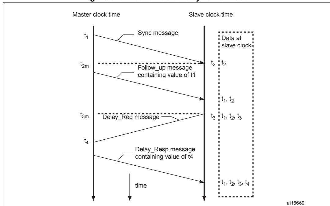
- 1. The master broadcasts PTP Sync messages to all its nodes. The Sync message contains the master's reference time information. The time at which this message leaves the master's system is \( t_1 \) . For Ethernet ports, this time has to be captured at the MII.
- 2. A slave receives the Sync message and also captures the exact time, \( t_2 \) , using its timing reference.
- 3. The master then sends the slave a Follow_up message, which contains the \( t_1 \) information for later use.
- 4. The slave sends the master a Delay_Req message, noting the exact time, \( t_3 \) , at which this frame leaves the MII.
- 5. The master receives this message and captures the exact time, \( t_4 \) , at which it enters its system.
- 6. The master sends the \( t_4 \) information to the slave in the Delay_Resp message.
- 7. The slave uses the four values of \( t_1 \) , \( t_2 \) , \( t_3 \) , and \( t_4 \) to synchronize its local timing reference to the master's timing reference.
Most of the protocol implementation occurs in the software, above the UDP layer. As described above, however, hardware support is required to capture the exact time when specific PTP packets enter or leave the Ethernet port at the MII. This timing information has to be captured and returned to the software for a proper, high-accuracy implementation of PTP.
Reference timing source
To get a snapshot of the time, the core requires a reference time in 64-bit format (split into two 32-bit channels, with the upper 32 bits providing time in seconds, and the lower 32 bits indicating time in nanoseconds) as defined in the IEEE 1588 specification.
The PTP reference clock input is used to internally generate the reference time (also called the System Time) and to capture time stamps. The frequency of this reference clock must
be greater than or equal to the resolution of time stamp counter. The synchronization accuracy target between the master node and the slaves is around 100 ns.
The generation, update and modification of the System Time are described in System Time correction methods .
The accuracy depends on the PTP reference clock input period, the characteristics of the oscillator (drift) and the frequency of the synchronization procedure.
Due to the synchronization from the Tx and Rx clock input domain to the PTP reference clock domain, the uncertainty on the time stamp latched value is 1 reference clock period. If we add the uncertainty due to resolution, we will add half the period for time stamping.
Transmission of frames with the PTP feature
When a frame's SFD is output on the MII, a time stamp is captured. Frames for which time stamp capture is required are controllable on a per-frame basis. In other words, each transmitted frame can be marked to indicate whether a time stamp must be captured or not for that frame. The transmitted frames are not processed to identify PTP frames. Frame control is exercised through the control bits in the transmit descriptor. Captured time stamps are returned to the application in the same way as the status is provided for frames. The time stamp is sent back along with the Transmit status of the frame, inside the corresponding transmit descriptor, thus connecting the time stamp automatically to the specific PTP frame. The 64-bit time stamp information is written back to the TDES2 and TDES3 fields, with TDES2 holding the time stamp's 32 least significant bits.
Reception of frames with the PTP feature
When the IEEE 1588 time stamping feature is enabled, the Ethernet MAC captures the time stamp of all frames received on the MII. The MAC provides the time stamp as soon as the frame reception is complete. Captured time stamps are returned to the application in the same way as the frame status is provided. The time stamp is sent back along with the Receive status of the frame, inside the corresponding receive descriptor. The 64-bit time stamp information is written back to the RDES2 and RDES3 fields, with RDES2 holding the time stamp's 32 least significant bits.
System Time correction methods
The 64-bit PTP time is updated using the PTP input reference clock, HCLK. This PTP time is used as a source to take snapshots (time stamps) of the Ethernet frames being transmitted or received at the MII. The System Time counter can be initialized or corrected using either the Coarse or the Fine correction method.
In the Coarse correction method, the initial value or the offset value is written to the Time stamp update register (refer to Section 29.8.3 ). For initialization, the System Time counter is written with the value in the Time stamp update registers, whereas for system time correction, the offset value (Time stamp update register) is added to or subtracted from the system time.
In the Fine correction method, the slave clock (reference clock) frequency drift with respect to the master clock (as defined in IEEE 1588) is corrected over a period of time, unlike in the Coarse correction method where it is corrected in a single clock cycle. The longer correction time helps maintain linear time and does not introduce drastic changes (or a large jitter) in the reference time between PTP Sync message intervals. In this method, an accumulator sums up the contents of the Addend register as shown in Figure 350 . The arithmetic carry that the accumulator generates is used as a pulse to increment the system time counter.
The accumulator and the addend are 32-bit registers. Here, the accumulator acts as a high-precision frequency multiplier or divider. Figure 350 shows this algorithm.
Figure 350. System time update using the Fine correction method
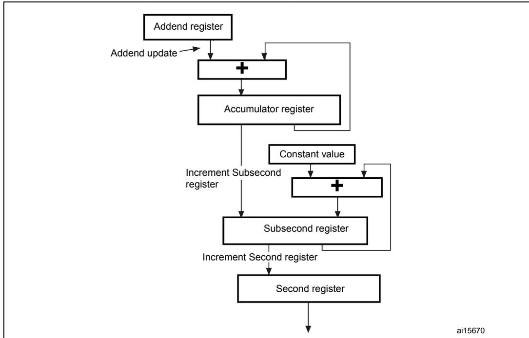
The system time update logic requires a 50 MHz clock frequency to achieve 20 ns accuracy. The frequency division is the ratio of the reference clock frequency to the required clock frequency. Hence, if the reference clock (HCLK) is, let us say, 66 MHz, the ratio is calculated as \( 66 \text{ MHz} / 50 \text{ MHz} = 1.32 \) . Hence, the default addend value to be set in the register is \( 2^{32} / 1.32 \) , which is equal to 0xC1F0 7C1F.
If the reference clock drifts lower, to 65 MHz for example, the ratio is \( 65 / 50 \) or 1.3 and the value to set in the addend register is \( 2^{32} / 1.30 \) equal to 0xC4EC 4EC4. If the clock drifts higher, to 67 MHz for example, the addend register must be set to 0xBF0 B7672. When the clock drift is zero, the default addend value of 0xC1F0 7C1F ( \( 2^{32} / 1.32 \) ) should be programmed.
In Figure 350 , the constant value used to increment the subsecond register is 0d43. This makes an accuracy of 20 ns in the system time (in other words, it is incremented by 20 ns steps).
The software has to calculate the drift in frequency based on the Sync messages, and to update the Addend register accordingly. Initially, the slave clock is set with FreqCompensationValue0 in the Addend register. This value is as follows:
If MasterToSlaveDelay is initially assumed to be the same for consecutive Sync messages, the algorithm described below must be applied. After a few Sync cycles, frequency lock occurs. The slave clock can then determine a precise MasterToSlaveDelay value and re-synchronize with the master using the new value.
The algorithm is as follows:
- • At time MasterSyncTime (n) the master sends the slave clock a Sync message. The slave receives this message when its local clock is SlaveClockTime (n) and computes MasterClockTime (n) as:\[ \text{MasterClockTime (n)} = \text{MasterSyncTime (n)} + \text{MasterToSlaveDelay (n)} \]
- • The master clock count for current Sync cycle, MasterClockCount (n) is given by:\[ \text{MasterClockCount (n)} = \text{MasterClockTime (n)} - \text{MasterClockTime (n - 1)} \](assuming that MasterToSlaveDelay is the same for Sync cycles n and n - 1)
- • The slave clock count for current Sync cycle, SlaveClockCount (n) is given by:\[ \text{SlaveClockCount (n)} = \text{SlaveClockTime (n)} - \text{SlaveClockTime (n - 1)} \]
- • The difference between master and slave clock counts for current Sync cycle, ClockDiffCount (n) is given by:\[ \text{ClockDiffCount (n)} = \text{MasterClockCount (n)} - \text{SlaveClockCount (n)} \]
- • The frequency-scaling factor for slave clock, FreqScaleFactor (n) is given by:\[ \text{FreqScaleFactor (n)} = (\text{MasterClockCount (n)} + \text{ClockDiffCount (n)}) / \text{SlaveClockCount (n)} \]
- • The frequency compensation value for Addend register, FreqCompensationValue (n) is given by:\[ \text{FreqCompensationValue (n)} = \text{FreqScaleFactor (n)} \times \text{FreqCompensationValue (n - 1)} \]
In theory, this algorithm achieves lock in one Sync cycle; however, it may take several cycles, due to changing network propagation delays and operating conditions.
This algorithm is self-correcting: if for any reason the slave clock is initially set to a value from the master that is incorrect, the algorithm corrects it at the cost of more Sync cycles.
Programming steps for system time generation initialization
The time stamping feature can be enabled by setting bit 0 in the Time stamp control register (ETH__PTPTSCR). However, it is essential to initialize the time stamp counter after this bit is set to start time stamp operation. The proper sequence is the following:
- 1. Mask the Time stamp trigger interrupt by setting bit 9 in the MACIMR register.
- 2. Program Time stamp register bit 0 to enable time stamping.
- 3. Program the Subsecond increment register based on the PTP clock frequency.
- 4. If you are using the Fine correction method, program the Time stamp addend register and set Time stamp control register bit 5 (addend register update).
- 5. Poll the Time stamp control register until bit 5 is cleared.
- 6. To select the Fine correction method (if required), program Time stamp control register bit 1.
- 7. Program the Time stamp high update and Time stamp low update registers with the appropriate time value.
- 8. Set Time stamp control register bit 2 (Time stamp init).
- 9. The Time stamp counter starts operation as soon as it is initialized with the value written in the Time stamp update register.
- 10. Enable the MAC receiver and transmitter for proper time stamping.
Note: If time stamp operation is disabled by clearing bit 0 in the ETH_PTPTSCR register, the above steps must be repeated to restart the time stamp operation.
Programming steps for system time update in the Coarse correction method
To synchronize or update the system time in one process (coarse correction method), perform the following steps:
- 1. Write the offset (positive or negative) in the Time stamp update high and low registers.
- 2. Set bit 3 (TSSTU) in the Time stamp control register.
- 3. The value in the Time stamp update registers is added to or subtracted from the system time when the TSSTU bit is cleared.
Programming steps for system time update in the Fine correction method
To synchronize or update the system time to reduce system-time jitter (fine correction method), perform the following steps:
- 1. With the help of the algorithm explained in System Time correction methods , calculate the rate by which you want to speed up or slow down the system time increments.
- 2. Update the time stamp.
- 3. Wait the time you want the new value of the Addend register to be active. You can do this by activating the Time stamp trigger interrupt after the system time reaches the target value.
- 4. Program the required target time in the Target time high and low registers. Unmask the Time stamp interrupt by clearing bit 9 in the ETH_MACIMR register.
- 5. Set Time stamp control register bit 4 (TSARU).
- 6. When this trigger causes an interrupt, read the ETH_MACSR register.
- 7. Reprogram the Time stamp addend register with the old value and set ETH_TPTSCR bit 5 again.
PTP trigger internal connection with TIM2
The MAC provides a trigger interrupt when the system time becomes greater than the target time. Using an interrupt introduces a known latency plus an uncertainty in the command execution time.
In order to avoid this uncertainty, a PTP trigger output signal is set high when the system time is greater than the target time. It is internally connected to the TIM2 input trigger. With this signal, the input capture feature, the output compare feature and the waveforms of the timer can be used, triggered by the synchronized PTP system time. No uncertainty is introduced since the clock of the timer (PCLK1: TIM2 APB1 clock) and PTP reference clock (HCLK) are synchronous.
This PTP trigger signal is connected to the TIM2 ITR1 input selectable by software. The connection is enabled through bit 29 in the AFIO_MAPR register. Figure 351 shows the connection.
Figure 351. PTP trigger output to TIM2 ITR1 connection
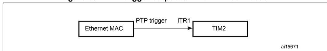
graph LR; A[Ethernet MAC] -- "PTP trigger" --> B[TIM2]; B -- "ITR1" --> A;
The diagram illustrates the internal connection between the Ethernet MAC and the TIM2 input trigger (ITR1). The Ethernet MAC outputs a PTP trigger signal to the TIM2 ITR1 input. The connection is shown as a line with arrows pointing to both components, labeled 'PTP trigger' and 'ITR1'. The diagram is enclosed in a box with the identifier 'ai15671' in the bottom right corner.
PTP pulse-per-second output signal
This PTP pulse output is used to check the synchronization between all nodes in the network. To be able to test the difference between the local slave clock and the master reference clock, both clocks were given a pulse-per-second (PPS) output signal that may be connected to an oscilloscope if necessary. The deviation between the two signals can therefore be measured. The pulse width of the PPS output is 125 ms.
The PPS output is enabled through bit 30 in the AFIO_MAPR register.
Figure 352. PPS output

The diagram shows a rectangular block labeled 'Ethernet MAC'. An arrow labeled 'PPS output' points from the right side of this block to the right edge of a larger outer rectangle. In the bottom right corner of the outer rectangle, the text 'ai15672' is present.
29.6 Ethernet functional description: DMA controller operation
The DMA has independent transmit and receive engines, and a CSR space. The transmit engine transfers data from system memory into the Tx FIFO while the receive engine transfers data from the Rx FIFO into system memory. The controller utilizes descriptors to efficiently move data from source to destination with minimum CPU intervention. The DMA is designed for packet-oriented data transfers such as frames in Ethernet. The controller can be programmed to interrupt the CPU in cases such as frame transmit and receive transfer completion, and other normal/error conditions. The DMA and the STM32F107xx communicate through two data structures:
- • Control and status registers (CSR)
- • Descriptor lists and data buffers.
Control and status registers are described in detail in Section 29.8 . Descriptors are described in detail in Tx DMA descriptors .
The DMA transfers the received data frames to the receive buffer in the STM32F107xx memory, and transmits data frames from the transmit buffer in the STM32F107xx memory. Descriptors that reside in the STM32F107xx memory act as pointers to these buffers. There are two descriptor lists: one for reception, and one for transmission. The base address of each list is written into DMA registers 3 and 4, respectively. A descriptor list is forward-linked (either implicitly or explicitly). The last descriptor may point back to the first entry to create a ring structure. Explicit chaining of descriptors is accomplished by configuring the second address chained in both the receive and transmit descriptors (RDES1[14] and TDES0[20]). The descriptor lists reside in the Host's physical memory space. Each descriptor can point to a maximum of two buffers. This enables the use of two physically addressed buffers, instead of two contiguous buffers in memory. A data buffer resides in the Host's physical memory space, and consists of an entire frame or part of a frame, but cannot exceed a single frame. Buffers contain only data. The buffer status is maintained in the descriptor. Data chaining refers to frames that span multiple data buffers. However, a single descriptor cannot span multiple frames. The DMA skips to the next frame buffer when the end of frame is detected. Data chaining can be enabled or disabled. The descriptor ring and chain structure is shown in Figure 353 .
Figure 353. Descriptor ring and chain structure
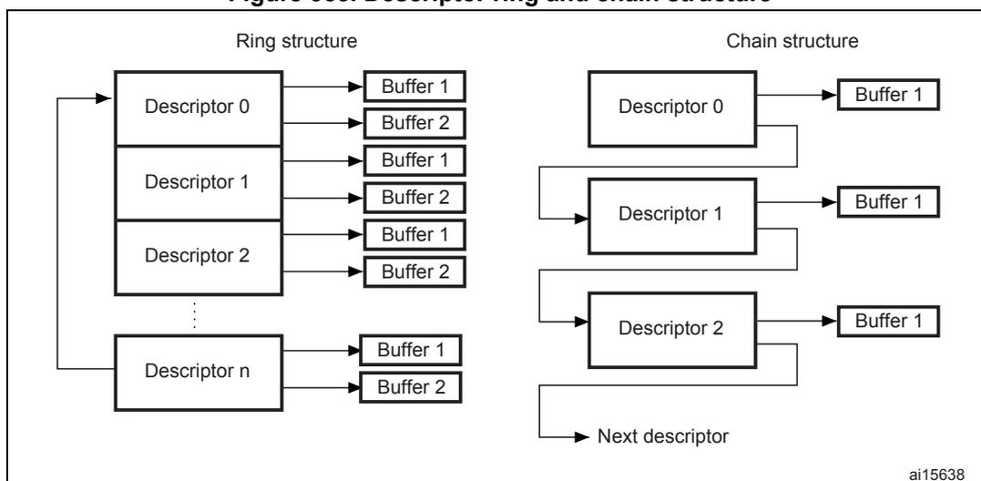
29.6.1 Initialization of a transfer using DMA
Initialization for the MAC is as follows:
- 1. Write to ETH_DMABMR to set STM32F107xx bus access parameters.
- 2. Write to the ETH_DMAIER register to mask unnecessary interrupt causes.
- 3. The software driver creates the transmit and receive descriptor lists. Then it writes to both the ETH_DMARDLAR and ETH_DMATDLAR registers, providing the DMA with the start address of each list.
- 4. Write to MAC registers 1, 2, and 3 to choose the desired filtering options.
- 5. Write to the MAC ETH_MACCR register to configure and enable the transmit and receive operating modes. The PS and DM bits are set based on the auto-negotiation result (read from the PHY).
- 6. Write to the ETH_DMAOMR register to set bits 13 and 1 and start transmission and reception.
- 7. The transmit and receive engines enter the running state and attempt to acquire descriptors from the respective descriptor lists. The receive and transmit engines then begin processing receive and transmit operations. The transmit and receive processes are independent of each other and can be started or stopped separately.
29.6.2 Host bus burst access
The DMA attempts to execute fixed-length burst transfers on the AHB master interface if configured to do so (FB bit in ETH_DMABMR). The maximum burst length is indicated and limited by the PBL field (ETH_DMABMR [13:8]). The receive and transmit descriptors are always accessed in the maximum possible burst size (limited by PBL) for the 16 bytes to be read.
The Transmit DMA initiates a data transfer only when there is sufficient space in the Transmit FIFO to accommodate the configured burst or the number of bytes until the end of frame (when it is less than the configured burst length). The DMA indicates the start address and the number of transfers required to the AHB Master Interface. When the AHB Interface is configured for fixed-length burst, then it transfers data using the best combination of
INCR4, INCR8, INCR16 and SINGLE transactions. Otherwise (no fixed-length burst), it transfers data using INCR (undefined length) and SINGLE transactions.
The Receive DMA initiates a data transfer only when sufficient data for the configured burst is available in Receive FIFO or when the end of frame (when it is less than the configured burst length) is detected in the Receive FIFO. The DMA indicates the start address and the number of transfers required to the AHB master interface. When the AHB interface is configured for fixed-length burst, then it transfers data using the best combination of INCR4, INCR8, INCR16 and SINGLE transactions. If the end of frame is reached before the fixed-burst ends on the AHB interface, then dummy transfers are performed in order to complete the fixed-length burst. Otherwise (FB bit in ETH_DMABMR is reset), it transfers data using INCR (undefined length) and SINGLE transactions.
When the AHB interface is configured for address-aligned beats, both DMA engines ensure that the first burst transfer the AHB initiates is less than or equal to the size of the configured PBL. Thus, all subsequent beats start at an address that is aligned to the configured PBL. The DMA can only align the address for beats up to size 16 (for PBL > 16), because the AHB interface does not support more than INCR16.
29.6.3 Host data buffer alignment
The transmit and receive data buffers do not have any restrictions on start address alignment. In our system with 32-bit memory, the start address for the buffers can be aligned to any of the four bytes. However, the DMA always initiates transfers with address aligned to the bus width with dummy data for the byte lanes not required. This typically happens during the transfer of the beginning or end of an Ethernet frame.
- • Example of buffer read:
If the Transmit buffer address is 0x0000 0FF2, and 15 bytes need to be transferred, then the DMA will read five full words from address 0x0000 0FF0, but when transferring data to the Transmit FIFO, the extra bytes (the first two bytes) will be dropped or ignored. Similarly, the last 3 bytes of the last transfer will also be ignored. The DMA always ensures it transfers a full 32-bit data items to the Transmit FIFO, unless it is the end of frame.
- • Example of buffer write:
If the Receive buffer address is 0x0000 0FF2, and 16 bytes of a received frame need to be transferred, then the DMA will write five full 32-bit data items from address 0x0000 0FF0. But the first 2 bytes of the first transfer and the last 2 bytes of the third transfer will have dummy data.
29.6.4 Buffer size calculations
The DMA does not update the size fields in the transmit and receive descriptors. The DMA updates only the status fields (xDES0) of the descriptors. The driver has to calculate the sizes. The transmit DMA transfers the exact number of bytes (indicated by buffer size field in TDES1) towards the MAC core. If a descriptor is marked as first (FS bit in TDES0 is set), then the DMA marks the first transfer from the buffer as the start of frame. If a descriptor is marked as last (LS bit in TDES0), then the DMA marks the last transfer from that data buffer as the end of frame. The receive DMA transfers data to a buffer until the buffer is full or the end of frame is received. If a descriptor is not marked as last (LS bit in RDES0), then the buffer(s) that correspond to the descriptor are full and the amount of valid data in a buffer is accurately indicated by the buffer size field minus the data buffer pointer offset when the descriptor's FS bit is set. The offset is zero when the data buffer pointer is aligned to the
databus width. If a descriptor is marked as last, then the buffer may not be full (as indicated by the buffer size in RDES1). To compute the amount of valid data in this final buffer, the driver must read the frame length (FL bits in RDES0[29:16]) and subtract the sum of the buffer sizes of the preceding buffers in this frame. The receive DMA always transfers the start of next frame with a new descriptor.
Note: Even when the start address of a receive buffer is not aligned to the system databus width the system should allocate a receive buffer of a size aligned to the system bus width. For example, if the system allocates a 1024 byte (1 KB) receive buffer starting from address 0x1000, the software can program the buffer start address in the receive descriptor to have a 0x1002 offset. The receive DMA writes the frame to this buffer with dummy data in the first two locations (0x1000 and 0x1001). The actual frame is written from location 0x1002. Thus, the actual useful space in this buffer is 1022 bytes, even though the buffer size is programmed as 1024 bytes, due to the start address offset.
29.6.5 DMA arbiter
The arbiter inside the DMA takes care of the arbitration between transmit and receive channel accesses to the AHB master interface. Two types of arbitrations are possible: round-robin, and fixed-priority. When round-robin arbitration is selected (DA bit in ETH_DMABMR is reset), the arbiter allocates the databus in the ratio set by the PM bits in ETH_DMABMR, when both transmit and receive DMAs request access simultaneously. When the DA bit is set, the receive DMA always gets priority over the transmit DMA for data access.
29.6.6 Error response to DMA
For any data transfer initiated by a DMA channel, if the slave replies with an error response, that DMA stops all operations and updates the error bits and the fatal bus error bit in the Status register (ETH_DMASR register). That DMA controller can resume operation only after soft- or hard-resetting the peripheral and re-initializing the DMA.
29.6.7 Tx DMA configuration
TxDMA operation: default (non-OSF) mode
The transmit DMA engine in default mode proceeds as follows:
- 1. The user sets up the transmit descriptor (TDES0-TDES3) and sets the OWN bit (TDES0[31]) after setting up the corresponding data buffer(s) with Ethernet frame data.
- 2. Once the ST bit (ETH_DMAOMR register[13]) is set, the DMA enters the Run state.
- 3. While in the Run state, the DMA polls the transmit descriptor list for frames requiring transmission. After polling starts, it continues in either sequential descriptor ring order or chained order. If the DMA detects a descriptor flagged as owned by the CPU, or if an error condition occurs, transmission is suspended and both the Transmit buffer Unavailable (ETH_DMASR register[2]) and Normal Interrupt Summary (ETH_DMASR register[16]) bits are set. The transmit engine proceeds to Step 9.
- 4. If the acquired descriptor is flagged as owned by DMA (TDES0[31] is set), the DMA decodes the transmit data buffer address from the acquired descriptor.
- 5. The DMA fetches the transmit data from the STM32F107xx memory and transfers the data.
- 6. If an Ethernet frame is stored over data buffers in multiple descriptors, the DMA closes the intermediate descriptor and fetches the next descriptor. Steps 3, 4, and 5 are repeated until the end of Ethernet frame data is transferred.
- 7. When frame transmission is complete, if IEEE 1588 time stamping was enabled for the frame (as indicated in the transmit status) the time stamp value is written to the transmit descriptor (TDES2 and TDES3) that contains the end-of-frame buffer. The status information is then written to this transmit descriptor (TDES0). Because the OWN bit is cleared during this step, the CPU now owns this descriptor. If time stamping was not enabled for this frame, the DMA does not alter the contents of TDES2 and TDES3.
- 8. Transmit Interrupt (ETH_DMASR register [0]) is set after completing the transmission of a frame that has Interrupt on Completion (TDES1[31]) set in its last descriptor. The DMA engine then returns to Step 3.
- 9. In the Suspend state, the DMA tries to re-acquire the descriptor (and thereby returns to Step 3) when it receives a transmit poll demand, and the Underflow Interrupt Status bit is cleared.
Figure 354 shows the TxDMA transmission flow in default mode.
Figure 354. TxDMA operation in Default mode
graph TD; Start[Start TxDMA] --> Stop[Stop TxDMA]; Stop -- Start --> Fetch[(Re-)fetch next descriptor]; Fetch --> AHB1{(AHB error?)}; AHB1 -- Yes --> Stop; AHB1 -- No --> OwnBit{Own bit set?}; OwnBit -- No --> Suspended[TxDMA suspended]; Suspended -- Poll demand --> Fetch; OwnBit -- Yes --> Transfer[Transfer data from buffer(s)]; Transfer --> AHB2{(AHB error?)}; AHB2 -- Yes --> Stop; AHB2 -- No --> FrameXfer{Frame xfer complete?}; FrameXfer -- No --> Close[Close intermediate descriptor]; Close --> Fetch; FrameXfer -- Yes --> WaitTx[Wait for Tx status]; WaitTx --> TimeStamp{Time stamp present?}; TimeStamp -- Yes --> WriteStamp[Write time stamp to TDES2 and TDES3]; TimeStamp -- No --> WriteStatus[Write status word to TDES0]; WriteStamp --> AHB3{(AHB error?)}; AHB3 -- Yes --> Stop; AHB3 -- No --> WriteStatus; WriteStatus --> AHB4{(AHB error?)}; AHB4 -- Yes --> Stop; AHB4 -- No --> Fetch;The flowchart illustrates the TxDMA operation in Default mode. It begins with 'Start TxDMA' leading to 'Stop TxDMA', which then leads to '(Re-)fetch next descriptor'. From there, it enters a loop: '(Re-)fetch next descriptor' leads to a decision '(AHB error?)'. If 'Yes', it goes to 'Stop TxDMA'. If 'No', it goes to 'Own bit set?'. If 'No', it goes to 'TxDMA suspended', which then goes to 'Poll demand' and back to '(Re-)fetch next descriptor'. If 'Yes', it goes to 'Transfer data from buffer(s)'. This leads to another '(AHB error?)' decision. If 'Yes', it goes to 'Stop TxDMA'. If 'No', it goes to 'Frame xfer complete?'. If 'No', it goes to 'Close intermediate descriptor' and back to '(Re-)fetch next descriptor'. If 'Yes', it goes to 'Wait for Tx status'. This leads to 'Time stamp present?'. If 'Yes', it goes to 'Write time stamp to TDES2 and TDES3'. If 'No', it goes to 'Write status word to TDES0'. Both lead to '(AHB error?)'. If 'Yes', it goes to 'Stop TxDMA'. If 'No', it goes to 'Write status word to TDES0' (from the 'Yes' path) or to '(AHB error?)' (from the 'No' path). If 'Yes', it goes to 'Stop TxDMA'. If 'No', it goes back to '(Re-)fetch next descriptor'.
TxDMA operation: OSF mode
While in the Run state, the transmit process can simultaneously acquire two frames without closing the Status descriptor of the first (if the OSF bit is set in ETH_DMAOMR register[2]). As the transmit process finishes transferring the first frame, it immediately polls the transmit descriptor list for the second frame. If the second frame is valid, the transmit process transfers this frame before writing the first frame's status information. In OSF mode, the Run-state transmit DMA operates according to the following sequence:
- 1. The DMA operates as described in steps 1–6 of the TxDMA (default mode).
- 2. Without closing the previous frame's last descriptor, the DMA fetches the next descriptor.
- 3. If the DMA owns the acquired descriptor, the DMA decodes the transmit buffer address in this descriptor. If the DMA does not own the descriptor, the DMA goes into Suspend mode and skips to Step 7.
- 4. The DMA fetches the Transmit frame from the STM32F107xx memory and transfers the frame until the end of frame data are transferred, closing the intermediate descriptors if this frame is split across multiple descriptors.
- 5. The DMA waits for the transmission status and time stamp of the previous frame. When the status is available, the DMA writes the time stamp to TDES2 and TDES3, if such time stamp was captured (as indicated by a status bit). The DMA then writes the status, with a cleared OWN bit, to the corresponding TDES0, thus closing the descriptor. If time stamping was not enabled for the previous frame, the DMA does not alter the contents of TDES2 and TDES3.
- 6. If enabled, the Transmit interrupt is set, the DMA fetches the next descriptor, then proceeds to Step 3 (when Status is normal). If the previous transmission status shows an underflow error, the DMA goes into Suspend mode (Step 7).
- 7. In Suspend mode, if a pending status and time stamp are received by the DMA, it writes the time stamp (if enabled for the current frame) to TDES2 and TDES3, then writes the status to the corresponding TDES0. It then sets relevant interrupts and returns to Suspend mode.
- 8. The DMA can exit Suspend mode and enter the Run state (go to Step 1 or Step 2 depending on pending status) only after receiving a Transmit Poll demand (ETH_DMATPDR register).
Figure 355 shows the basic flowchart in OSF mode.
Figure 355. TxDMA operation in OSF mode
graph TD
    Start[Start TxDMA] -- Start --> Fetch["(Re-)fetch next descriptor"]
    Stop[Stop TxDMA] --> Fetch
    Fetch --> AHB1{"(AHB) error?"}
    AHB1 -- Yes --> Stop
    AHB1 -- No --> Own{"Own bit set?"}
    Own -- No --> Suspended[TxDMA suspended]
    Own -- Yes --> Transfer["Transfer data from buffer(s)"]
    Transfer --> AHB2{"(AHB) error?"}
    AHB2 -- Yes --> Stop
    AHB2 -- No --> Complete{"Frame xfer complete?"}
    Complete -- No --> Close[Close intermediate descriptor]
    Complete -- Yes --> Second{"Second frame?"}
    Second -- Yes --> Wait["Wait for previous frame's Tx status"]
    Second -- No --> Close
    Wait --> WriteStamp["Write time stamp to TDES2 & TDES3 for previous frame"]
    Close --> TimeStamp1{"Time stamp present?"}
    TimeStamp1 -- Yes --> WriteStamp
    TimeStamp1 -- No --> WriteStatus1["Write status word to prev. frame's TDES0"]
    WriteStamp --> AHB3{"(AHB) error?"}
    AHB3 -- Yes --> Stop
    AHB3 -- No --> WriteStatus1
    WriteStatus1 --> AHB4{"(AHB) error?"}
    AHB4 -- Yes --> Stop
    AHB4 -- No --> Fetch
    Suspended -- Poll demand --> Fetch
    Suspended -- Previous frame status available --> TimeStamp2{"Time stamp present?"}
    TimeStamp2 -- Yes --> WriteStamp
    TimeStamp2 -- No --> WriteStatus2["Write status word to prev. frame's TDES0"]
    WriteStatus2 --> AHB5{"(AHB) error?"}
    AHB5 -- Yes --> Stop
    AHB5 -- No --> Suspended
Transmit frame processing
The transmit DMA expects that the data buffers contain complete Ethernet frames, excluding preamble, pad bytes, and FCS fields. The DA, SA, and Type/Len fields contain valid data. If the transmit descriptor indicates that the MAC core must disable CRC or pad insertion, the buffer must have complete Ethernet frames (excluding preamble), including the CRC bytes. Frames can be data-chained and span over several buffers. Frames have to be delimited by the first descriptor (TDES0[28]) and the last descriptor (TDES0[29]). As the transmission starts, TDES0[28] has to be set in the first descriptor. When this occurs, the frame data are transferred from the memory buffer to the Transmit FIFO. Concurrently, if the last descriptor (TDES0[29]) of the current frame is cleared, the transmit process attempts to acquire the next descriptor. The transmit process expects TDES0[28] to be cleared in this descriptor. If TDES0[29] is cleared, it indicates an intermediary buffer. If TDES0[29] is set, it
indicates the last buffer of the frame. After the last buffer of the frame has been transmitted, the DMA writes back the final status information to the transmit descriptor 0 (TDES0) word of the descriptor that has the last segment set in transmit descriptor 0 (TDES0[29]). At this time, if Interrupt on Completion (TDES0[30]) is set, Transmit Interrupt (in ETH_DMASR register [0]) is set, the next descriptor is fetched, and the process repeats. Actual frame transmission begins after the Transmit FIFO has reached either a programmable transmit threshold (ETH_DMAOMR register[16:14]), or a full frame is contained in the FIFO. There is also an option for the Store and forward mode (ETH_DMAOMR register[21]). Descriptors are released (OWN bit TDES0[31] is cleared) when the DMA finishes transferring the frame.
Transmit polling suspended
Transmit polling can be suspended by either of the following conditions:
- • The DMA detects a descriptor owned by the CPU (TDES0[31]=0) and the Transmit buffer unavailable flag is set (ETH_DMASR register[2]). To resume, the driver must give descriptor ownership to the DMA and then issue a Poll Demand command.
- • A frame transmission is aborted when a transmit error due to underflow is detected. The appropriate Transmit Descriptor 0 (TDES0) bit is set. If the second condition occurs, both the Abnormal Interrupt Summary (in ETH_DMASR register [15]) and Transmit Underflow bits (in ETH_DMASR register[5]) are set, and the information is written to Transmit Descriptor 0, causing the suspension. If the DMA goes into Suspend state due to the first condition, then both the Normal Interrupt Summary (ETH_DMASR register [16]) and Transmit Buffer Unavailable (ETH_DMASR register[2]) bits are set. In both cases, the position in the transmit list is retained. The retained position is that of the descriptor following the last descriptor closed by the DMA. The driver must explicitly issue a Transmit Poll Demand command after rectifying the suspension cause.
Tx DMA descriptors
The descriptor structure consists of four 32-bit words as shown in Figure 356. The bit descriptions of TDES0, TDES1, TDES2 and TDES3 are given below.
Figure 356. Transmit descriptor
| 31 | 0 | ||||||||
|---|---|---|---|---|---|---|---|---|---|
| TDES 0 | OWN | Ctrl [30:26] | T T S E | Res. 24 | Ctrl [23:20] | Reserved [19:18] | T T S S | Status [16:0] | |
| TDES 1 | Reserved [31:29] | Buffer 2 byte count [28:16] | Reserved [15:13] | Buffer 1 byte count [12:0] | |||||
| TDES 2 | Buffer 1 address [31:0] / Time stamp low [31:0] | ||||||||
| TDES 3 | Buffer 2 address [31:0] or Next descriptor address [31:0] / Time stamp high [31:0] | ||||||||
ai15642b
- • TDES0: Transmit descriptor Word0
The application software has to program the control bits [30:26]+[23:20] plus the OWN bit [31] during descriptor initialization. When the DMA updates the descriptor (or writes it back), it resets all the control bits plus the OWN bit, and reports only the status bits.
| 31 | 30 | 29 | 28 | 27 | 26 | 25 | 24 | 23 | 22 | 21 | 20 | 19 | 18 | 17 | 16 |
|---|---|---|---|---|---|---|---|---|---|---|---|---|---|---|---|
| OWN | IC | LS | FS | DC | DP | TTSE | Res | CIC | TER | TCH | Res. | TTSS | IHE | ||
| r/w | r/w | r/w | r/w | r/w | r/w | r/w | r/w | r/w | r/w | r/w | r/w | r/w | |||
| 15 | 14 | 13 | 12 | 11 | 10 | 9 | 8 | 7 | 6 | 5 | 4 | 3 | 2 | 1 | 0 |
| ES | JT | FF | IPE | LCA | NC | LCO | EC | VF | CC | ED | UF | DB | |||
| r/w | r/w | r/w | r/w | r/w | r/w | r/w | r/w | r/w | r/w | r/w | r/w | r/w | r/w | r/w | |
Bit 31 OWN : Own bit
When set, this bit indicates that the descriptor is owned by the DMA. When this bit is reset, it indicates that the descriptor is owned by the CPU. The DMA clears this bit either when it completes the frame transmission or when the buffers allocated in the descriptor are read completely. The ownership bit of the frame's first descriptor must be set after all subsequent descriptors belonging to the same frame have been set.
Bit 30 IC : Interrupt on completion
When set, this bit sets the Transmit Interrupt (ETH_DMASR[0]) after the present frame has been transmitted.
Bit 29 LS : Last segment
When set, this bit indicates that the buffer contains the last segment of the frame.
Bit 28 FS : First segment
When set, this bit indicates that the buffer contains the first segment of a frame.
Bit 27 DC : Disable CRC
When this bit is set, the MAC does not append a cyclic redundancy check (CRC) to the end of the transmitted frame. This is valid only when the first segment (TDES0[28]) is set.
Bit 26 DP : Disable pad
When set, the MAC does not automatically add padding to a frame shorter than 64 bytes. When this bit is reset, the DMA automatically adds padding and CRC to a frame shorter than 64 bytes, and the CRC field is added despite the state of the DC (TDES0[27]) bit. This is valid only when the first segment (TDES0[28]) is set.
Bit 25 TTSE : Transmit time stamp enable
When TTSE is set and when TSE is set (ETH_PTPSCR bit 0), IEEE1588 hardware time stamping is activated for the transmit frame described by the descriptor. This field is only valid when the First segment control bit (TDES0[28]) is set.
Bit 24 Reserved, must be kept at reset value.
Bits 23:22 CIC : Checksum insertion control
These bits control the checksum calculation and insertion. Bit encoding is as shown below:
00: Checksum Insertion disabled
01: Only IP header checksum calculation and insertion are enabled
10: IP header checksum and payload checksum calculation and insertion are enabled, but pseudo-header checksum is not calculated in hardware
11: IP Header checksum and payload checksum calculation and insertion are enabled, and pseudo-header checksum is calculated in hardware.
Bit 21 TER : Transmit end of ring
When set, this bit indicates that the descriptor list reached its final descriptor. The DMA returns to the base address of the list, creating a descriptor ring.
Bit 20 TCH : Second address chained
When set, this bit indicates that the second address in the descriptor is the next descriptor address rather than the second buffer address. When TDES0[20] is set, TBS2 (TDES1[28:16]) is a “don’t care” value. TDES0[21] takes precedence over TDES0[20].
Bits 19:18 Reserved, must be kept at reset value.
Bit 17 TTSS : Transmit time stamp status
This field is used as a status bit to indicate that a time stamp was captured for the described transmit frame. When this bit is set, TDES2 and TDES3 have a time stamp value captured for the transmit frame. This field is only valid when the descriptor’s Last segment control bit (TDES0[29]) is set.
Bit 16 IHE : IP header error
When set, this bit indicates that the MAC transmitter detected an error in the IP datagram header. The transmitter checks the header length in the IPv4 packet against the number of header bytes received from the application and indicates an error status if there is a mismatch. For IPv6 frames, a header error is reported if the main header length is not 40 bytes. Furthermore, the Ethernet length/type field value for an IPv4 or IPv6 frame must match the IP header version received with the packet. For IPv4 frames, an error status is also indicated if the Header Length field has a value less than 0x5.
Bit 15 ES : Error summary
Indicates the logical OR of the following bits:
- TDES0[14]: Jabber timeout
- TDES0[13]: Frame flush
- TDES0[11]: Loss of carrier
- TDES0[10]: No carrier
- TDES0[9]: Late collision
- TDES0[8]: Excessive collision
- TDES0[2]: Excessive deferral
- TDES0[1]: Underflow error
- TDES0[16]: IP header error
- TDES0[12]: IP payload error
Bit 14 JT : Jabber timeout
When set, this bit indicates the MAC transmitter has experienced a jabber timeout. This bit is only set when the MAC configuration register’s JD bit is not set.
Bit 13 FF : Frame flushed
When set, this bit indicates that the DMA/MTL flushed the frame due to a software Flush command given by the CPU.
Bit 12 IPE : IP payload error
When set, this bit indicates that MAC transmitter detected an error in the TCP, UDP, or ICMP IP datagram payload. The transmitter checks the payload length received in the IPv4 or IPv6 header against the actual number of TCP, UDP or ICMP packet bytes received from the application and issues an error status in case of a mismatch.
Bit 11 LCA : Loss of carrier
When set, this bit indicates that a loss of carrier occurred during frame transmission (that is, the MII_CRS signal was inactive for one or more transmit clock periods during frame transmission). This is valid only for the frames transmitted without collision when the MAC operates in Half-duplex mode.
Bit 10 NC : No carrierWhen set, this bit indicates that the Carrier Sense signal from the PHY was not asserted during transmission.
Bit 9 LCO : Late collisionWhen set, this bit indicates that frame transmission was aborted due to a collision occurring after the collision window (64 byte times, including preamble, in MII mode). This bit is not valid if the Underflow Error bit is set.
Bit 8 EC : Excessive collisionWhen set, this bit indicates that the transmission was aborted after 16 successive collisions while attempting to transmit the current frame. If the RD (Disable retry) bit in the MAC Configuration register is set, this bit is set after the first collision, and the transmission of the frame is aborted.
Bit 7 VF : VLAN frameWhen set, this bit indicates that the transmitted frame was a VLAN-type frame.
Bits 6:3 CC : Collision countThis 4-bit counter value indicates the number of collisions occurring before the frame was transmitted. The count is not valid when the Excessive collisions bit (TDES0[8]) is set.
Bit 2 ED : Excessive deferralWhen set, this bit indicates that the transmission has ended because of excessive deferral of over 24 288 bit times if the Deferral check (DC) bit in the MAC Control register is set high.
Bit 1 UF : Underflow errorWhen set, this bit indicates that the MAC aborted the frame because data arrived late from the RAM memory. Underflow error indicates that the DMA encountered an empty transmit buffer while transmitting the frame. The transmission process enters the Suspended state and sets both Transmit underflow (ETH_DMASR[5]) and Transmit interrupt (ETH_DMASR[0]).
Bit 0 DB : Deferred bitWhen set, this bit indicates that the MAC defers before transmission because of the presence of the carrier. This bit is valid only in Half-duplex mode.
- • TDES1: Transmit descriptor Word1

| 31 | 30 | 29 | 28 | 27 | 26 | 25 | 24 | 23 | 22 | 21 | 20 | 19 | 18 | 17 | 16 | 15 | 14 | 13 | 12 | 11 | 10 | 9 | 8 | 7 | 6 | 5 | 4 | 3 | 2 | 1 | 0 |
| Reserved | TBS2 | Reserved | TBS1 | ||||||||||||||||||||||||||||
| rw | rw | rw | rw | rw | rw | rw | rw | rw | rw | rw | rw | rw | rw | rw | rw | rw | rw | rw | rw | rw | rw | rw | rw | rw | rw | rw | rw | rw | rw | rw | rw |
31:29 Reserved, must be kept at reset value.
28:16 TBS2 : Transmit buffer 2 sizeThese bits indicate the second data buffer size in bytes. This field is not valid if TDES0[20] is set.
15:13 Reserved, must be kept at reset value.
12:0 TBS1 : Transmit buffer 1 sizeThese bits indicate the first data buffer byte size, in bytes. If this field is 0, the DMA ignores this buffer and uses Buffer 2 or the next descriptor, depending on the value of TCH (TDES0[20]).
- • TDES2: Transmit descriptor Word2
TDES2 contains the address pointer to the first buffer of the descriptor or it contains time stamp data.

| 31 | 30 | 29 | 28 | 27 | 26 | 25 | 24 | 23 | 22 | 21 | 20 | 19 | 18 | 17 | 16 | 15 | 14 | 13 | 12 | 11 | 10 | 9 | 8 | 7 | 6 | 5 | 4 | 3 | 2 | 1 | 0 |
| TBAP1/TBAP/TTSL | |||||||||||||||||||||||||||||||
| rw | |||||||||||||||||||||||||||||||
Bits 31:0 TBAP1 : Transmit buffer 1 address pointer / Transmit frame time stamp low
These bits have two different functions: they indicate to the DMA the location of data in memory, and after all data are transferred, the DMA can then use these bits to pass back time stamp data.
TBAP : When the software makes this descriptor available to the DMA (at the moment that the OWN bit is set to 1 in TDES0), these bits indicate the physical address of Buffer 1. There is no limitation on the buffer address alignment. See Host data buffer alignment for further details on buffer address alignment.
TTSL : Before it clears the OWN bit in TDES0, the DMA updates this field with the 32 least significant bits of the time stamp captured for the corresponding transmit frame (overwriting the value for TBAP1). This field has the time stamp only if time stamping is activated for this frame (see TTSE, TDES0 bit 25) and if the Last segment control bit (LS) in the descriptor is set.
- • TDES3: Transmit descriptor Word3
TDES3 contains the address pointer either to the second buffer of the descriptor or the next descriptor, or it contains time stamp data.

| 31 | 30 | 29 | 28 | 27 | 26 | 25 | 24 | 23 | 22 | 21 | 20 | 19 | 18 | 17 | 16 | 15 | 14 | 13 | 12 | 11 | 10 | 9 | 8 | 7 | 6 | 5 | 4 | 3 | 2 | 1 | 0 |
| TBAP2/TBAP2/TTSH | |||||||||||||||||||||||||||||||
| rw | |||||||||||||||||||||||||||||||
Bits 31:0 TBAP2 : Transmit buffer 2 address pointer (Next descriptor address) / Transmit frame time stamp high
These bits have two different functions: they indicate to the DMA the location of data in memory, and after all data are transferred, the DMA can then use these bits to pass back time stamp data.
TBAP2 : When the software makes this descriptor available to the DMA (at the moment when the OWN bit is set to 1 in TDES0), these bits indicate the physical address of Buffer 2 when a descriptor ring structure is used. If the Second address chained (TDES1 [20]) bit is set, this address contains the pointer to the physical memory where the next descriptor is present. The buffer address pointer must be aligned to the bus width only when TDES1 [20] is set. (LSBs are ignored internally.)
TTSH : Before it clears the OWN bit in TDES0, the DMA updates this field with the 32 most significant bits of the time stamp captured for the corresponding transmit frame (overwriting the value for TBAP2). This field has the time stamp only if time stamping is activated for this frame (see TDES0 bit 25, TTSE) and if the Last segment control bit (LS) in the descriptor is set.
29.6.8 Rx DMA configuration
The Receive DMA engine's reception sequence is illustrated in Figure 357 and described below:
- 1. The CPU sets up Receive descriptors (RDES0-RDES3) and sets the OWN bit (RDES0[31]).
- 2. Once the SR (ETH_DMAOMR register[1]) bit is set, the DMA enters the Run state. While in the Run state, the DMA polls the receive descriptor list, attempting to acquire free descriptors. If the fetched descriptor is not free (is owned by the CPU), the DMA enters the Suspend state and jumps to Step 9.
- 3. The DMA decodes the receive data buffer address from the acquired descriptors.
- 4. Incoming frames are processed and placed in the acquired descriptor's data buffers.
- 5. When the buffer is full or the frame transfer is complete, the Receive engine fetches the next descriptor.
- 6. If the current frame transfer is complete, the DMA proceeds to step 7. If the DMA does not own the next fetched descriptor and the frame transfer is not complete (EOF is not yet transferred), the DMA sets the Descriptor error bit in RDES0 (unless flushing is disabled). The DMA closes the current descriptor (clears the OWN bit) and marks it as intermediate by clearing the Last segment (LS) bit in the RDES1 value (marks it as last descriptor if flushing is not disabled), then proceeds to step 8. If the DMA owns the next descriptor but the current frame transfer is not complete, the DMA closes the current descriptor as intermediate and returns to step 4.
- 7. If IEEE 1588 time stamping is enabled, the DMA writes the time stamp (if available) to the current descriptor's RDES2 and RDES3. It then takes the received frame's status and writes the status word to the current descriptor's RDES0, with the OWN bit cleared and the Last segment bit set.
- 8. The Receive engine checks the latest descriptor's OWN bit. If the CPU owns the descriptor (OWN bit is at 0) the Receive buffer unavailable bit (in ETH_DMASR register[7]) is set and the DMA Receive engine enters the Suspended state (step 9). If the DMA owns the descriptor, the engine returns to step 4 and awaits the next frame.
- 9. Before the Receive engine enters the Suspend state, partial frames are flushed from the Receive FIFO (you can control flushing using bit 24 in the ETH_DMAOMR register).
- 10. The Receive DMA exits the Suspend state when a Receive Poll demand is given or the start of next frame is available from the Receive FIFO. The engine proceeds to step 2 and re-fetches the next descriptor.
The DMA does not acknowledge accepting the status until it has completed the time stamp write-back and is ready to perform status write-back to the descriptor. If software has enabled time stamping through CSR, when a valid time stamp value is not available for the frame (for example, because the receive FIFO was full before the time stamp could be written to it), the DMA writes all ones to RDES2 and RDES3. Otherwise (that is, if time stamping is not enabled), RDES2 and RDES3 remain unchanged.
Figure 357. Receive DMA operation
graph TD; Start[Start RxDMA] --> Fetch[(Re-)Fetch next descriptor]; Stop[Stop RxDMA] --> Fetch; Fetch --> Error1{(AHB error?)}; Error1 -- Yes --> Stop; Error1 -- No --> OwnBit{Own bit set?}; OwnBit -- Yes --> DataAvail{Frame data available?}; OwnBit -- No --> TransferComplete{Frame transfer complete?}; TransferComplete -- No --> Error1; TransferComplete -- Yes --> FlushDisabled{Flush disabled?}; FlushDisabled -- Yes --> Suspended[RxDMA suspended]; Suspended --> Fetch; FlushDisabled -- No --> Flush[Flush the remaining frame]; Flush --> Fetch; DataAvail -- No --> Wait[Wait for frame data]; Wait --> Fetch; DataAvail -- Yes --> Write[Write data to buffer(s)]; Write --> Error2{(AHB error?)}; Error2 -- Yes --> Stop; Error2 -- No --> NextDesc[Fetch next descriptor]; NextDesc --> Error3{(AHB error?)}; Error3 -- Yes --> Stop; Error3 -- No --> TransferComplete2{Frame transfer complete?}; TransferComplete2 -- No --> OwnBit2{Own bit set for next desc?}; OwnBit2 -- Yes --> FlushDisabled2{Flush disabled?}; OwnBit2 -- No --> TransferComplete2; FlushDisabled2 -- Yes --> SetError[Set descriptor error]; SetError --> CloseRDES0[Close RDES0 as intermediate descriptor]; CloseRDES0 --> CloseLast[Close RDES0 as last descriptor]; CloseLast --> Error4{(AHB error?)}; Error4 -- Yes --> Stop; Error4 -- No --> Timestamp{Time stamp present?}; Timestamp -- Yes --> WriteStamp[Write time stamp to RDES2 & RDES3]; WriteStamp --> CloseLast; Timestamp -- No --> CloseLast;ai15643
Receive descriptor acquisition
The receive engine always attempts to acquire an extra descriptor in anticipation of an incoming frame. Descriptor acquisition is attempted if any of the following conditions is/are satisfied:
- • The receive Start/Stop bit (ETH_DMAOMR register[1]) has been set immediately after the DMA has been placed in the Run state.
- • The data buffer of the current descriptor is full before the end of the frame currently being transferred
- • The controller has completed frame reception, but the current receive descriptor has not yet been closed.
- • The receive process has been suspended because of a CPU-owned buffer (RDES0[31] = 0) and a new frame is received.
- • A Receive poll demand has been issued.
Receive frame processing
The MAC transfers the received frames to the STM32F107xx memory only when the frame passes the address filter and the frame size is greater than or equal to the configurable threshold bytes set for the Receive FIFO, or when the complete frame is written to the FIFO in Store-and-forward mode. If the frame fails the address filtering, it is dropped in the MAC block itself (unless Receive All ETH_MACFFR [31] bit is set). Frames that are shorter than 64 bytes, because of collision or premature termination, can be purged from the Receive FIFO. After 64 (configurable threshold) bytes have been received, the DMA block begins transferring the frame data to the receive buffer pointed to by the current descriptor. The DMA sets the first descriptor (RDES0[9]) after the DMA AHB Interface becomes ready to receive a data transfer (if DMA is not fetching transmit data from the memory), to delimit the frame. The descriptors are released when the OWN (RDES0[31]) bit is reset to 0, either as the data buffer fills up or as the last segment of the frame is transferred to the receive buffer. If the frame is contained in a single descriptor, both the last descriptor (RDES0[8]) and first descriptor (RDES0[9]) bits are set. The DMA fetches the next descriptor, sets the last descriptor (RDES0[8]) bit, and releases the RDES0 status bits in the previous frame descriptor. Then the DMA sets the receive interrupt bit (ETH_DMASR register [6]). The same process repeats unless the DMA encounters a descriptor flagged as being owned by the CPU. If this occurs, the receive process sets the receive buffer unavailable bit (ETH_DMASR register[7]) and then enters the Suspend state. The position in the receive list is retained.
Receive process suspended
If a new receive frame arrives while the receive process is in Suspend state, the DMA re-fetches the current descriptor in the STM32F107xx memory. If the descriptor is now owned by the DMA, the receive process re-enters the Run state and starts frame reception. If the descriptor is still owned by the host, by default, the DMA discards the current frame at the top of the Rx FIFO and increments the missed frame counter. If more than one frame is stored in the Rx FIFO, the process repeats. The discarding or flushing of the frame at the top of the Rx FIFO can be avoided by setting the DMA Operation mode register bit 24 (DFRF). In such conditions, the receive process sets the receive buffer unavailable status bit and returns to the Suspend state.
Rx DMA descriptors
The descriptor structure consists of four 32-bit words (16 bytes). These are shown in Figure 358. The bit descriptions of RDES0, RDES1, RDES2 and RDES3 are given below.
Figure 358. Rx DMA descriptor structure
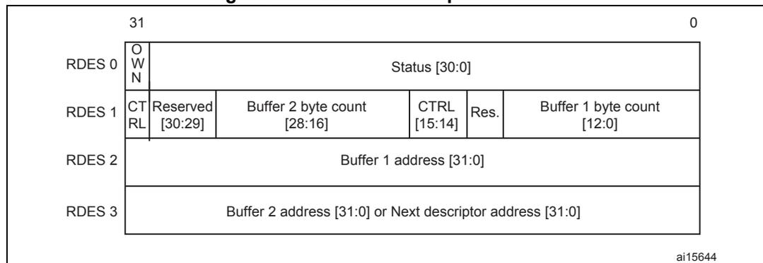
| 31 | 0 | |||||
| RDES 0 | O W N | Status [30:0] | ||||
| RDES 1 | CTRL | Reserved [30:29] | Buffer 2 byte count [28:16] | CTRL [15:14] | Res. | Buffer 1 byte count [12:0] |
| RDES 2 | Buffer 1 address [31:0] | |||||
| RDES 3 | Buffer 2 address [31:0] or Next descriptor address [31:0] | |||||
ai15644
- RDES0: Receive descriptor Word0
RDES0 contains the received frame status, the frame length and the descriptor ownership information.
| 31 | 30 | 29 | 28 | 27 | 26 | 25 | 24 | 23 | 22 | 21 | 20 | 19 | 18 | 17 | 16 | 15 | 14 | 13 | 12 | 11 | 10 | 9 | 8 | 7 | 6 | 5 | 4 | 3 | 2 | 1 | 0 |
| OWN | AFM | FL | ES | DE | SAF | LE | OE | VLAN | FS | LS | IPHCE | LCO | FT | RWT | RE | DE | CE | PCE | |||||||||||||
| rw | |||||||||||||||||||||||||||||||
Bit 31 OWN : Own bit
When set, this bit indicates that the descriptor is owned by the DMA of the MAC Subsystem. When this bit is reset, it indicates that the descriptor is owned by the Host. The DMA clears this bit either when it completes the frame reception or when the buffers that are associated with this descriptor are full.
Bit 30 AFM : Destination address filter fail
When set, this bit indicates a frame that failed the DA filter in the MAC Core.
Bits 29:16 FL : Frame length
These bits indicate the byte length of the received frame that was transferred to host memory (including CRC). This field is valid only when last descriptor (RDES0[8]) is set and descriptor error (RDES0[14]) is reset.
This field is valid when last descriptor (RDES0[8]) is set. When the last descriptor and error summary bits are not set, this field indicates the accumulated number of bytes that have been transferred for the current frame.
Bit 15 ES: Error summaryIndicates the logical OR of the following bits:
RDES0[1]: CRC error
RDES0[3]: Receive error
RDES0[4]: Watchdog timeout
RDES0[6]: Late collision
RDES0[7]: Giant frame (This is not applicable when RDES0[7] indicates an IPv4 header checksum error.)
RDES0[11]: Overflow error
RDES0[14]: Descriptor error.
This field is valid only when the last descriptor (RDES0[8]) is set.
Bit 14 DE: Descriptor errorWhen set, this bit indicates a frame truncation caused by a frame that does not fit within the current descriptor buffers, and that the DMA does not own the next descriptor. The frame is truncated.
This field is valid only when the last descriptor (RDES0[8]) is set.
Bit 13 SAF: Source address filter failWhen set, this bit indicates that the SA field of frame failed the SA filter in the MAC Core.
Bit 12 LE: Length errorWhen set, this bit indicates that the actual length of the received frame does not match the value in the Length/ Type field. This bit is valid only when the Frame type (RDES0[5]) bit is reset.
Bit 11 OE: Overflow errorWhen set, this bit indicates that the received frame was damaged due to buffer overflow.
Bit 10 VLAN: VLAN tagWhen set, this bit indicates that the frame pointed to by this descriptor is a VLAN frame tagged by the MAC core.
Bit 9 FS: First descriptorWhen set, this bit indicates that this descriptor contains the first buffer of the frame. If the size of the first buffer is 0, the second buffer contains the beginning of the frame. If the size of the second buffer is also 0, the next descriptor contains the beginning of the frame.
Bit 8 LS: Last descriptorWhen set, this bit indicates that the buffers pointed to by this descriptor are the last buffers of the frame.
Bit 7 IPHCE: IPv header checksum errorIf IPHCE is set, it indicates an error in the IPv4 or IPv6 header. This error can be due to inconsistent Ethernet Type field and IP header Version field values, a header checksum mismatch in IPv4, or an Ethernet frame lacking the expected number of IP header bytes.
Bit 6 LCO: Late collisionWhen set, this bit indicates that a late collision has occurred while receiving the frame in Half-duplex mode.
Bit 5 FT: Frame typeWhen set, this bit indicates that the Receive frame is an Ethernet-type frame (the LT field is greater than or equal to 0x0600). When this bit is reset, it indicates that the received frame is an IEEE802.3 frame. This bit is not valid for Runt frames less than 14 bytes.
Bit 4 RWT: Receive watchdog timeoutWhen set, this bit indicates that the Receive watchdog timer has expired while receiving the current frame and the current frame is truncated after the watchdog timeout.
Bit 3 RE : Receive error
When set, this bit indicates that the RX_ERR signal is asserted while RX_DV is asserted during frame reception.
Bit 2 DE : Dribble bit error
When set, this bit indicates that the received frame has a non-integer multiple of bytes (odd nibbles). This bit is valid only in MII mode.
Bit 1 CE : CRC error
When set, this bit indicates that a cyclic redundancy check (CRC) error occurred on the received frame. This field is valid only when the last descriptor (RDES0[8]) is set.
Bit 0 PCE : Payload checksum error
When set, it indicates that the TCP, UDP or ICMP checksum the core calculated does not match the received encapsulated TCP, UDP or ICMP segment's Checksum field. This bit is also set when the received number of payload bytes does not match the value indicated in the Length field of the encapsulated IPv4 or IPv6 datagram in the received Ethernet frame.
Bits 5, 7, and 0 reflect the conditions discussed in Table 217.
Table 217. Receive descriptor 0
| Bit 5: frame type | Bit 7: IPC checksum error | Bit 0: payload checksum error | Frame status |
|---|---|---|---|
| 0 | 0 | 0 | IEEE 802.3 Type frame (Length field value is less than 0x0600.) |
| 1 | 0 | 0 | IPv4/IPv6 Type frame, no checksum error detected |
| 1 | 0 | 1 | IPv4/IPv6 Type frame with a payload checksum error (as described for PCE) detected |
| 1 | 1 | 0 | IPv4/IPv6 Type frame with an IP header checksum error (as described for IPC CE) detected |
| 1 | 1 | 1 | IPv4/IPv6 Type frame with both IP header and payload checksum errors detected |
| 0 | 0 | 1 | IPv4/IPv6 Type frame with no IP header checksum error and the payload check bypassed, due to an unsupported payload |
| 0 | 1 | 1 | A Type frame that is neither IPv4 or IPv6 (the checksum offload engine bypasses checksum completely.) |
| 0 | 1 | 0 | Reserved |
• RDES1: Receive descriptor Word1
| 31 | 30 | 29 | 28 | 27 | 26 | 25 | 24 | 23 | 22 | 21 | 20 | 19 | 18 | 17 | 16 | 15 | 14 | 13 | 12 | 11 | 10 | 9 | 8 | 7 | 6 | 5 | 4 | 3 | 2 | 1 | 0 |
|---|---|---|---|---|---|---|---|---|---|---|---|---|---|---|---|---|---|---|---|---|---|---|---|---|---|---|---|---|---|---|---|
| DIC | RBS2 | RER | RCH | Reserved | RBS | ||||||||||||||||||||||||||
| rw | rw | rw | rw | rw | rw | rw | rw | rw | rw | rw | rw | rw | rw | rw | rw | rw | rw | rw | rw | rw | rw | rw | rw | rw | rw | rw | rw | rw | rw | rw | |
Bit 31 DIC : Disable interrupt on completion
When set, this bit prevents setting the Status register's RS bit (CSR5[6]) for the received frame ending in the buffer indicated by this descriptor. This, in turn, disables the assertion of the interrupt to Host due to RS for that frame.
Bits 30:29 Reserved, must be kept at reset value.
Bits 28:16 RBS2 : Receive buffer 2 size
These bits indicate the second data buffer size, in bytes. The buffer size must be a multiple of 4, 8, or 16, depending on the bus widths (32, 64 or 128, respectively), even if the value of RDES3 (buffer2 address pointer) is not aligned to bus width. If the buffer size is not an appropriate multiple of 4, 8 or 16, the resulting behavior is undefined. This field is not valid if RDES1[14] is set.
Bit 15 RER : Receive end of ring
When set, this bit indicates that the descriptor list reached its final descriptor. The DMA returns to the base address of the list, creating a descriptor ring.
Bit 14 RCH : Second address chained
When set, this bit indicates that the second address in the descriptor is the next descriptor address rather than the second buffer address. When this bit is set, RBS2 (RDES1[28:16]) is a "don't care" value. RDES1[15] takes precedence over RDES1[14].
Bit 13 Reserved, must be kept at reset value.
Bits 12:0 RBS1 : Receive buffer 1 size
Indicates the first data buffer size in bytes. The buffer size must be a multiple of 4, 8 or 16, depending upon the bus widths (32, 64 or 128), even if the value of RDES2 (buffer1 address pointer) is not aligned. When the buffer size is not a multiple of 4, 8 or 16, the resulting behavior is undefined. If this field is 0, the DMA ignores this buffer and uses Buffer 2 or next descriptor depending on the value of RCH (bit 14).
- • RDES2: Receive descriptor Word2
RDES2 contains the address pointer to the first data buffer in the descriptor, or it contains time stamp data.

| 31 | 30 | 29 | 28 | 27 | 26 | 25 | 24 | 23 | 22 | 21 | 20 | 19 | 18 | 17 | 16 | 15 | 14 | 13 | 12 | 11 | 10 | 9 | 8 | 7 | 6 | 5 | 4 | 3 | 2 | 1 | 0 |
| RBP1 / RTSL | |||||||||||||||||||||||||||||||
| rw | rw | rw | rw | rw | rw | rw | rw | rw | rw | rw | rw | rw | rw | rw | rw | rw | rw | rw | rw | rw | rw | rw | rw | rw | rw | rw | rw | rw | rw | rw | rw |
Bits 31:0 RBAP1 / RTSL : Receive buffer 1 address pointer / Receive frame time stamp low
These bits take on two different functions: the application uses them to indicate to the DMA where to store the data in memory, and then after transferring all the data the DMA may use these bits to pass back time stamp data.
RBAP1 : When the software makes this descriptor available to the DMA (at the moment that the OWN bit is set to 1 in RDES0), these bits indicate the physical address of Buffer 1. There are no limitations on the buffer address alignment except for the following condition: the DMA uses the configured value for its address generation when the RDES2 value is used to store the start of frame. Note that the DMA performs a write operation with the RDES2[3/2/1:0] bits as 0 during the transfer of the start of frame but the frame data is shifted as per the actual buffer address pointer. The DMA ignores RDES2[3/2/1:0] (corresponding to bus width of 128/64/32) if the address pointer is to a buffer where the middle or last part of the frame is stored.
RTSL : Before it clears the OWN bit in RDES0, the DMA updates this field with the 32 least significant bits of the time stamp captured for the corresponding receive frame (overwriting the value for RBAP1). This field has the time stamp only if time stamping is activated for this frame and if the Last segment control bit (LS) in the descriptor is set.
- • RDES3: Receive descriptor Word3
RDES3 contains the address pointer either to the second data buffer in the descriptor or to the next descriptor, or it contains time stamp data.

| 31 | 30 | 29 | 28 | 27 | 26 | 25 | 24 | 23 | 22 | 21 | 20 | 19 | 18 | 17 | 16 | 15 | 14 | 13 | 12 | 11 | 10 | 9 | 8 | 7 | 6 | 5 | 4 | 3 | 2 | 1 | 0 |
| RBP2 / RTSH | |||||||||||||||||||||||||||||||
| rw | rw | rw | rw | rw | rw | rw | rw | rw | rw | rw | rw | rw | rw | rw | rw | rw | rw | rw | rw | rw | rw | rw | rw | rw | rw | rw | rw | rw | rw | rw | rw |
Bits 31:0 RBAP2 / RTSH : Receive buffer 2 address pointer (next descriptor address) / Receive frame time stamp high
These bits take on two different functions: the application uses them to indicate to the DMA the location of where to store the data in memory, and then after transferring all the data the DMA may use these bits to pass back time stamp data.
RBAP1 : When the software makes this descriptor available to the DMA (at the moment that the OWN bit is set to 1 in RDES0), these bits indicate the physical address of buffer 2 when a descriptor ring structure is used. If the second address chained (RDES1 [24]) bit is set, this address contains the pointer to the physical memory where the next descriptor is present. If RDES1 [24] is set, the buffer (next descriptor) address pointer must be bus width-aligned (RDES3[3, 2, or 1:0] = 0, corresponding to a bus width of 128, 64 or 32. LSBs are ignored internally.) However, when RDES1 [24] is reset, there are no limitations on the RDES3 value, except for the following condition: the DMA uses the configured value for its buffer address generation when the RDES3 value is used to store the start of frame. The DMA ignores RDES3[3, 2, or 1:0] (corresponding to a bus width of 128, 64 or 32) if the address pointer is to a buffer where the middle or last part of the frame is stored.
RTSH : Before it clears the OWN bit in RDES0, the DMA updates this field with the 32 most significant bits of the time stamp captured for the corresponding receive frame (overwriting the value for RBAP2). This field has the time stamp only if time stamping is activated and if the Last segment control bit (LS) in the descriptor is set.
29.6.9 DMA interrupts
Interrupts can be generated as a result of various events. The ETH_DMASR register contains all the bits that might cause an interrupt. The ETH_DMAIER register contains an enable bit for each of the events that can cause an interrupt.
There are two groups of interrupts, Normal and Abnormal, as described in the ETH_DMASR register. Interrupts are cleared by writing a 1 to the corresponding bit position. When all the enabled interrupts within a group are cleared, the corresponding summary bit is cleared. If the MAC core is the cause for assertion of the interrupt, then any of the TSTS or PMTS bits in the ETH_DMASR register is set high.
Interrupts are not queued and if the interrupt event occurs before the driver has responded to it, no additional interrupts are generated. For example, the Receive Interrupt bit (ETH_DMASR register [6]) indicates that one or more frames were transferred to the STM32F107xx buffer. The driver must scan all descriptors, from the last recorded position to the first one owned by the DMA.
An interrupt is generated only once for simultaneous, multiple events. The driver must scan the ETH_DMASR register for the cause of the interrupt. The interrupt is not generated again unless a new interrupting event occurs, after the driver has cleared the appropriate bit in the ETH_DMASR register. For example, the controller generates a Receive interrupt (ETH_DMASR register[6]) and the driver begins reading the ETH_DMASR register. Next, receive buffer unavailable (ETH_DMASR register[7]) occurs. The driver clears the Receive
interrupt. Even then, a new interrupt is generated, due to the active or pending Receive buffer unavailable interrupt.
Figure 359. Interrupt scheme
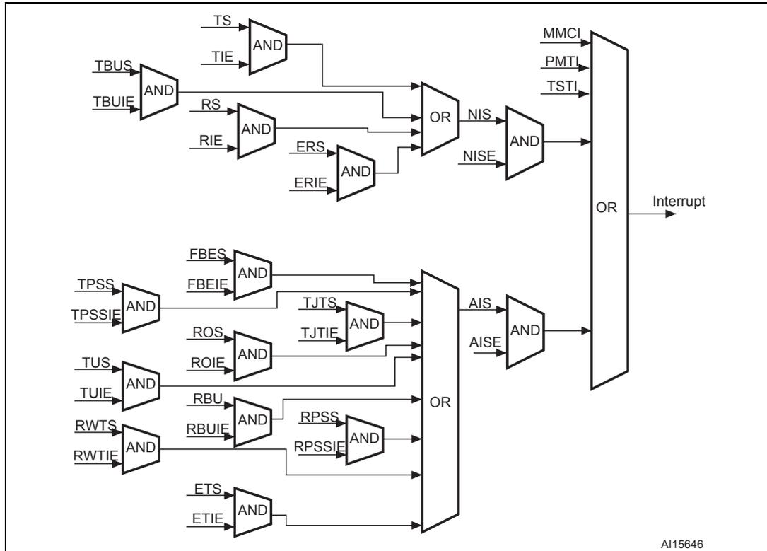
The diagram illustrates the interrupt scheme for the Ethernet MAC. It consists of several stages of AND and OR gates that combine various status and enable signals to generate a final interrupt signal.
- Top Path (Normal Interrupts):
- Inputs: TS, TIE, TBUS, TBUFE, RS, RIE, ERS, ERIE.
- Logic: TS and TIE are ANDed. TBUS and TBUFE are ANDed. RS and RIE are ANDed. ERS and ERIE are ANDed. The outputs of the RS/RIE and ERS/ERIE AND gates are ORed. This result is ANDed with the output of the TBUS/TBUFE AND gate. The output of this AND gate is ORed with the output of the TS/TIE AND gate. This combined result is ANDed with NIS (Network Interrupt Status). The output of this AND gate is then ORed with the output of a large multi-input OR gate (described below) to produce the final Interrupt signal.
- Bottom Path (Wake-up Interrupts):
- Inputs: TPSS, TPSSIE, FBE, FBEIE, ROS, ROIE, TUS, TUIE, RBU, RBUFE, RWTS, RWTIE, ETS, ETIE.
- Logic: TPSS and TPSSIE are ANDed. FBE and FBEIE are ANDed. ROS and ROIE are ANDed. TUS and TUIE are ANDed. RBU and RBUFE are ANDed. RWTS and RWTIE are ANDed. ETS and ETIE are ANDed. The outputs of the TPSS/TPSSIE, ROS/ROIE, RBU/RBUFE, RWTS/RWTIE, and ETS/ETIE AND gates are ORed. The output of the FBE/FBEIE AND gate is ANDed with TJTS and TJTIE. The outputs of the main OR gate and the TJTS/TJTIE AND gate are ORed. This result is ANDed with AIS (Activity Interrupt Status). The output of this AND gate is then ORed with the output of the top path to produce the final Interrupt signal.
- Additional Inputs: MMCI, PMTI, and TSTI are also inputs to the final OR gate that generates the Interrupt signal.
29.7 Ethernet interrupts
The Ethernet controller has two interrupt vectors: one dedicated to normal Ethernet operations and the other, used only for the Ethernet wakeup event (with wakeup frame or Magic Packet detection) when it is mapped on EXTI line19.
The first Ethernet vector is reserved for interrupts generated by the MAC and the DMA as listed in the MAC interrupts and DMA interrupts sections.
The second vector is reserved for interrupts generated by the PMT on wakeup events. The mapping of a wakeup event on EXTI line19 causes the STM32F107xx to exit the low-power mode, and generates an interrupt.
When an Ethernet wakeup event mapped on EXTI Line19 occurs and the MAC PMT interrupt is enabled and the EXTI Line19 interrupt, with detection on rising edge, is also enabled, both interrupts are generated.
A watchdog timer (see ETH_DMARSWTR register) is given for flexible control of the RS bit (ETH_DMASR register). When this watchdog timer is programmed with a non-zero value, it gets activated as soon as the RxDMA completes a transfer of a received frame to system memory without asserting the Receive Status because it is not enabled in the corresponding Receive descriptor (RDES1[31]). When this timer runs out as per the programmed value, the RS bit is set and the interrupt is asserted if the corresponding RIE is enabled in the
ETH_DMAIER register. This timer is disabled before it runs out, when a frame is transferred to memory and the RS is set because it is enabled for that descriptor.
Note: Reading the PMT control and status register automatically clears the Wakeup Frame Received and Magic Packet Received PMT interrupt flags. However, since the registers for these flags are in the CLK_RX domain, there may be a significant delay before this update is visible by the firmware. The delay is especially long when the RX clock is slow (in 10 Mbit mode) and when the AHB bus is high-frequency. Since interrupt requests from the PMT to the CPU are based on the same registers in the CLK_RX domain, the CPU may spuriously call the interrupt routine a second time even after reading PMT_CSR. Thus, it may be necessary that the firmware polls the Wakeup Frame Received and Magic Packet Received bits and exits the interrupt service routine only when they are found to be at '0'.
29.8 Ethernet register descriptions
The peripheral registers can be accessed by bytes (8-bit), half-words (16-bit) or words (32-bits).
29.8.1 MAC register description
Ethernet MAC configuration register (ETH_MACCR)
Address offset: 0x0000
Reset value: 0x0000 8000
The MAC configuration register is the operation mode register of the MAC. It establishes receive and transmit operating modes.
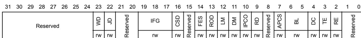
| 31 | 30 | 29 | 28 | 27 | 26 | 25 | 24 | 23 | 22 | 21 | 20 | 19 | 18 | 17 | 16 | 15 | 14 | 13 | 12 | 11 | 10 | 9 | 8 | 7 | 6 | 5 | 4 | 3 | 2 | 1 | 0 |
| Reserved | WD | JD | Reserved | IFG | CSD | Reserved | FLS | ROD | LM | DM | IPCO | RD | Reserved | APCS | BL | DC | TE | RE | Reserved | ||||||||||||
| rw | rw | rw | rw | rw | rw | rw | rw | rw | rw | rw | rw | rw | |||||||||||||||||||
Bits 31:24 Reserved, must be kept at reset value.
Bit 23 WD : Watchdog disable
When this bit is set, the MAC disables the watchdog timer on the receiver, and can receive frames of up to 16 384 bytes.
When this bit is reset, the MAC allows no more than 2 048 bytes of the frame being received and cuts off any bytes received after that.
Bit 22 JD : Jabber disable
When this bit is set, the MAC disables the jabber timer on the transmitter, and can transfer frames of up to 16 384 bytes.
When this bit is reset, the MAC cuts off the transmitter if the application sends out more than 2 048 bytes of data during transmission.
Bits 21:20 Reserved, must be kept at reset value.
Bits 19:17 IFG : Interframe gap
These bits control the minimum interframe gap between frames during transmission.
000: 96 bit times
001: 88 bit times
010: 80 bit times
...
111: 40 bit times
Note: In Half-duplex mode, the minimum IFG can be configured for 64 bit times (IFG = 100) only. Lower values are not considered.
Bit 16 CSD : Carrier sense disable
When set high, this bit makes the MAC transmitter ignore the MII CRS signal during frame transmission in Half-duplex mode. No error is generated due to Loss of Carrier or No Carrier during such transmission.
When this bit is low, the MAC transmitter generates such errors due to Carrier Sense and even aborts the transmissions.
Bit 15 Reserved, must be kept at reset value.
Bit 14 FES : Fast Ethernet speed
Indicates the speed in Fast Ethernet (MII) mode:
0: 10 Mbit/s
1: 100 Mbit/s
Bit 13 ROD : Receive own disable
When this bit is set, the MAC disables the reception of frames in Half-duplex mode.
When this bit is reset, the MAC receives all packets that are given by the PHY while transmitting.
This bit is not applicable if the MAC is operating in Full-duplex mode.
Bit 12 LM : Loopback mode
When this bit is set, the MAC operates in loopback mode at the MII. The MII receive clock input (RX_CLK) is required for the loopback to work properly, as the transmit clock is not looped-back internally.
Bit 11 DM : Duplex mode
When this bit is set, the MAC operates in a Full-duplex mode where it can transmit and receive simultaneously.
Bit 10 IPCO : IPv4 checksum offload
When set, this bit enables IPv4 checksum checking for received frame payloads' TCP/UDP/ICMP headers. When this bit is reset, the checksum offload function in the receiver is disabled and the corresponding PCE and IP HCE status bits (see Table 214 ) are always cleared.
Bit 9 RD : Retry disable
When this bit is set, the MAC attempts only 1 transmission. When a collision occurs on the MII, the MAC ignores the current frame transmission and reports a Frame Abort with excessive collision error in the transmit frame status.
When this bit is reset, the MAC attempts retries based on the settings of BL.
Note: This bit is applicable only in the Half-duplex mode.
Bit 8 Reserved, must be kept at reset value.
Bit 7 APCS: Automatic pad/CRC strippingWhen this bit is set, the MAC strips the Pad/FCS field on incoming frames only if the length's field value is less than or equal to 1 500 bytes. All received frames with length field greater than or equal to 1 501 bytes are passed on to the application without stripping the Pad/FCS field.
When this bit is reset, the MAC passes all incoming frames unmodified.
Bits 6:5 BL: Back-off limitThe Back-off limit determines the random integer number ( \( r \) ) of slot time delays (4 096 bit times for 1000 Mbit/s and 512 bit times for 10/100 Mbit/s) the MAC waits before rescheduling a transmission attempt during retries after a collision.
Note: This bit is applicable only to Half-duplex mode.
00: \( k = \min(n, 10) \)
01: \( k = \min(n, 8) \)
10: \( k = \min(n, 4) \)
11: \( k = \min(n, 1) \) ,
where \( n \) = retransmission attempt. The random integer \( r \) takes the value in the range \( 0 \leq r < 2^k \)
Bit 4 DC: Deferral checkWhen this bit is set, the deferral check function is enabled in the MAC. The MAC issues a Frame Abort status, along with the excessive deferral error bit set in the transmit frame status when the transmit state machine is deferred for more than 24 288 bit times in 10/100-Mbit/s mode. Deferral begins when the transmitter is ready to transmit, but is prevented because of an active CRS (carrier sense) signal on the MII. Defer time is not cumulative. If the transmitter defers for 10 000 bit times, then transmits, collides, backs off, and then has to defer again after completion of back-off, the deferral timer resets to 0 and restarts.
When this bit is reset, the deferral check function is disabled and the MAC defers until the CRS signal goes inactive. This bit is applicable only in Half-duplex mode.
Bit 3 TE: Transmitter enableWhen this bit is set, the transmit state machine of the MAC is enabled for transmission on the MII. When this bit is reset, the MAC transmit state machine is disabled after the completion of the transmission of the current frame, and does not transmit any further frames.
Bit 2 RE: Receiver enableWhen this bit is set, the receiver state machine of the MAC is enabled for receiving frames from the MII. When this bit is reset, the MAC receive state machine is disabled after the completion of the reception of the current frame, and will not receive any further frames from the MII.
Bits 1:0 Reserved, must be kept at reset value.
Ethernet MAC frame filter register (ETH_MACFFR)
Address offset: 0x0004
Reset value: 0x0000 0000
The MAC frame filter register contains the filter controls for receiving frames. Some of the controls from this register go to the address check block of the MAC, which performs the first level of address filtering. The second level of filtering is performed on the incoming frame, based on other controls such as pass bad frames and pass control frames.

| 31 | 30 | 29 | 28 | 27 | 26 | 25 | 24 | 23 | 22 | 21 | 20 | 19 | 18 | 17 | 16 | 15 | 14 | 13 | 12 | 11 | 10 | 9 | 8 | 7 | 6 | 5 | 4 | 3 | 2 | 1 | 0 | |
| RA | Reserved | HPF | SAF | SAIF | PCF | BFD | PAM | DAIF | HM | HU | PM | |||||||||||||||||||||
| rw | rw | rw | rw | rw | rw | rw | rw | rw | rw | rw | ||||||||||||||||||||||
Bit 31 RA: Receive all
When this bit is set, the MAC receiver passes all received frames on to the application, irrespective of whether they have passed the address filter. The result of the SA/DA filtering is updated (pass or fail) in the corresponding bits in the receive status word. When this bit is reset, the MAC receiver passes on to the application only those frames that have passed the SA/DA address filter.
Bits 30:11 Reserved, must be kept at reset value.
Bit 10 HPF: Hash or perfect filter
When this bit is set and if the HM or HU bit is set, the address filter passes frames that match either the perfect filtering or the hash filtering.
When this bit is cleared and if the HU or HM bit is set, only frames that match the Hash filter are passed.
Bit 9 SAF: Source address filter
The MAC core compares the SA field of the received frames with the values programmed in the enabled SA registers. If the comparison matches, then the SAMatch bit in the RxStatus word is set high. When this bit is set high and the SA filter fails, the MAC drops the frame. When this bit is reset, the MAC core forwards the received frame to the application. It also forwards the updated SA Match bit in RxStatus depending on the SA address comparison.
Bit 8 SAIF: Source address inverse filtering
When this bit is set, the address check block operates in inverse filtering mode for the SA address comparison. The frames whose SA matches the SA registers are marked as failing the SA address filter.
When this bit is reset, frames whose SA does not match the SA registers are marked as failing the SA address filter.
Bits 7:6 PCF: Pass control frames
These bits control the forwarding of all control frames (including unicast and multicast PAUSE frames). Note that the processing of PAUSE control frames depends only on RFCE in Flow Control register[2].
00 or 01: MAC prevents all control frames from reaching the application
10: MAC forwards all control frames to application even if they fail the address filter
11: MAC forwards control frames that pass the address filter.
Bit 5 BFD: Broadcast frames disable
When this bit is set, the address filters filter all incoming broadcast frames.
When this bit is reset, the address filters pass all received broadcast frames.
Bit 4 PAM : Pass all multicastWhen set, this bit indicates that all received frames with a multicast destination address (first bit in the destination address field is '1') are passed.
When reset, filtering of multicast frame depends on the HM bit.
When this bit is set, the address check block operates in inverse filtering mode for the DA address comparison for both unicast and multicast frames.
When reset, normal filtering of frames is performed.
When set, MAC performs destination address filtering of received multicast frames according to the hash table.
When reset, the MAC performs a perfect destination address filtering for multicast frames, that is, it compares the DA field with the values programmed in DA registers.
When set, MAC performs destination address filtering of unicast frames according to the hash table.
When reset, the MAC performs a perfect destination address filtering for unicast frames, that is, it compares the DA field with the values programmed in DA registers.
When this bit is set, the address filters pass all incoming frames regardless of their destination or source address. The SA/DA filter fails status bits in the receive status word are always cleared when PM is set.
Ethernet MAC hash table high register (ETH_MACHTHR)
Address offset: 0x0008
Reset value: 0x0000 0000
The 64-bit Hash table is used for group address filtering. For hash filtering, the contents of the destination address in the incoming frame are passed through the CRC logic, and the upper 6 bits in the CRC register are used to index the contents of the Hash table. This CRC is a 32-bit value coded by the following polynomial (for more details refer to Section 29.5.3 ):
The most significant bit determines the register to be used (hash table high/hash table low), and the other 5 bits determine which bit within the register. A hash value of 0b0 0000 selects bit 0 in the selected register, and a value of 0b1 1111 selects bit 31 in the selected register.
For example, if the DA of the incoming frame is received as 0x1F52 419C B6AF (0x1F is the first byte received on the MII interface), then the internally calculated 6-bit Hash value is 0x2C and the HTH register bit[12] is checked for filtering. If the DA of the incoming frame is received as 0xA00A 9800 0045, then the calculated 6-bit Hash value is 0x07 and the HTL register bit[7] is checked for filtering.
If the corresponding bit value in the register is 1, the frame is accepted. Otherwise, it is rejected. If the PAM (pass all multicast) bit is set in the ETH_MACFFR register, then all multicast frames are accepted regardless of the multicast hash values.
The Hash table high register contains the higher 32 bits of the multicast Hash table.

| 31 | 30 | 29 | 28 | 27 | 26 | 25 | 24 | 23 | 22 | 21 | 20 | 19 | 18 | 17 | 16 | 15 | 14 | 13 | 12 | 11 | 10 | 9 | 8 | 7 | 6 | 5 | 4 | 3 | 2 | 1 | 0 |
| HTH | |||||||||||||||||||||||||||||||
| rw | rw | rw | rw | rw | rw | rw | rw | rw | rw | rw | rw | rw | rw | rw | rw | rw | rw | rw | rw | rw | rw | rw | rw | rw | rw | rw | rw | rw | rw | rw | rw |
Bits 31:0
HTH
: Hash table high
This field contains the upper 32 bits of Hash table.
Ethernet MAC hash table low register (ETH_MACHTLR)
Address offset: 0x000C
Reset value: 0x0000 0000
The Hash table low register contains the lower 32 bits of the multi-cast Hash table.

| 31 | 30 | 29 | 28 | 27 | 26 | 25 | 24 | 23 | 22 | 21 | 20 | 19 | 18 | 17 | 16 | 15 | 14 | 13 | 12 | 11 | 10 | 9 | 8 | 7 | 6 | 5 | 4 | 3 | 2 | 1 | 0 |
| HTL | |||||||||||||||||||||||||||||||
| rw | rw | rw | rw | rw | rw | rw | rw | rw | rw | rw | rw | rw | rw | rw | rw | rw | rw | rw | rw | rw | rw | rw | rw | rw | rw | rw | rw | rw | rw | rw | rw |
Bits 31:0
HTL
: Hash table low
This field contains the lower 32 bits of the Hash table.
Ethernet MAC MII address register (ETH_MACMIAR)
Address offset: 0x0010
Reset value: 0x0000 0000
The MII address register controls the management cycles to the external PHY through the management interface.

| 31 | 30 | 29 | 28 | 27 | 26 | 25 | 24 | 23 | 22 | 21 | 20 | 19 | 18 | 17 | 16 | 15 | 14 | 13 | 12 | 11 | 10 | 9 | 8 | 7 | 6 | 5 | 4 | 3 | 2 | 1 | 0 |
| Reserved | PA | MR | Reserved | CR | MW | MB | |||||||||||||||||||||||||
| rw | rw | rw | rw | rw | rw | rw | rw | rw | rw | rw | rw | rw | rw | rc_w1 | |||||||||||||||||
Bits 31:16 Reserved, must be kept at reset value.
Bits 15:11
PA
: PHY address
This field tells which of the 32 possible PHY devices are being accessed.
Bits 10:6
MR
: MII register
These bits select the desired MII register in the selected PHY device.
Bit 5 Reserved, must be kept at reset value.
Bits 4:2
CR: Clock range
The CR clock range selection determines the HCLK frequency and is used to decide the frequency of the MDC clock:
Selection HCLK MDC Clock
000 60-72 MHz HCLK/42
001 Reserved -
010 20-35 MHz HCLK/16
011 35-60 MHz HCLK/26
100, 101, 110, 111 Reserved -
When set, this bit tells the PHY that this will be a Write operation using the MII Data register. If this bit is not set, this will be a Read operation, placing the data in the MII Data register.
Bit 0 MB : MII busyThis bit should read a logic 0 before writing to ETH_MACMIIAR and ETH_MACMIIDR. This bit must also be reset to 0 during a Write to ETH_MACMIIAR. During a PHY register access, this bit is set to 0b1 by the application to indicate that a read or write access is in progress. ETH_MACMIIDR (MII Data) should be kept valid until this bit is cleared by the MAC during a PHY Write operation. The ETH_MACMIIDR is invalid until this bit is cleared by the MAC during a PHY Read operation. The ETH_MACMIIAR (MII Address) should not be written to until this bit is cleared.
Ethernet MAC MII data register (ETH_MACMIIDR)Address offset: 0x0014
Reset value: 0x0000 0000
The MAC MII Data register stores write data to be written to the PHY register located at the address specified in ETH_MACMIIAR. ETH_MACMIIDR also stores read data from the PHY register located at the address specified by ETH_MACMIIAR.

| 31 | 30 | 29 | 28 | 27 | 26 | 25 | 24 | 23 | 22 | 21 | 20 | 19 | 18 | 17 | 16 | 15 | 14 | 13 | 12 | 11 | 10 | 9 | 8 | 7 | 6 | 5 | 4 | 3 | 2 | 1 | 0 |
|---|---|---|---|---|---|---|---|---|---|---|---|---|---|---|---|---|---|---|---|---|---|---|---|---|---|---|---|---|---|---|---|
| Reserved | MD | ||||||||||||||||||||||||||||||
| rw | rw | rw | rw | rw | rw | rw | rw | rw | rw | rw | rw | rw | rw | rw | rw | ||||||||||||||||
Bits 31:16 Reserved, must be kept at reset value.
Bits 15:0 MD : MII dataThis contains the 16-bit data value read from the PHY after a Management Read operation, or the 16-bit data value to be written to the PHY before a Management Write operation.
Ethernet MAC flow control register (ETH_MACFCR)Address offset: 0x0018
Reset value: 0x0000 0000
The Flow control register controls the generation and reception of the control (Pause Command) frames by the MAC. A write to a register with the Busy bit set to '1' causes the MAC to generate a pause control frame. The fields of the control frame are selected as specified in the 802.3x specification, and the Pause Time value from this register is used in the Pause Time field of the control frame. The Busy bit remains set until the control frame is transferred onto the cable. The Host must make sure that the Busy bit is cleared before writing to the register.
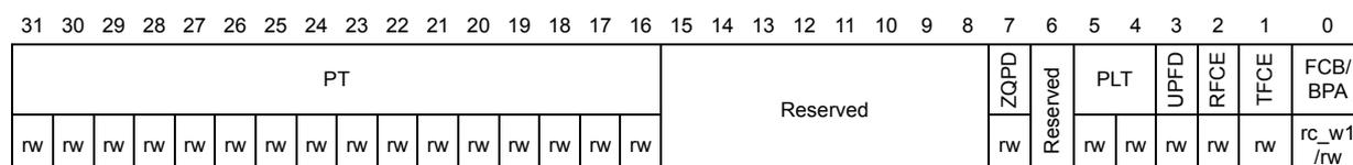
| 31 | 30 | 29 | 28 | 27 | 26 | 25 | 24 | 23 | 22 | 21 | 20 | 19 | 18 | 17 | 16 | 15 | 14 | 13 | 12 | 11 | 10 | 9 | 8 | 7 | 6 | 5 | 4 | 3 | 2 | 1 | 0 |
|---|---|---|---|---|---|---|---|---|---|---|---|---|---|---|---|---|---|---|---|---|---|---|---|---|---|---|---|---|---|---|---|
| PT | Reserved | ZQPD | Reserved | PLT | UPFD | RFCE | TFCE | FCB/ BPA | |||||||||||||||||||||||
| rw | rw | rw | rw | rw | rw | rw | rw | rw | rw | rw | rw | rw | rw | rw | rw | rw | rw | rw | rw | rw | rw | rc_w1 /rw | |||||||||
This field holds the value to be used in the Pause Time field in the transmit control frame. If the Pause Time bits is configured to be double-synchronized to the MII clock domain, then consecutive write operations to this register should be performed only after at least 4 clock cycles in the destination clock domain.
Bits 15:8 Reserved, must be kept at reset value.
Bit 7 ZQPD : Zero-quanta pause disableWhen set, this bit disables the automatic generation of Zero-quanta pause control frames on the deassertion of the flow-control signal from the FIFO layer.
When this bit is reset, normal operation with automatic Zero-quanta pause control frame generation is enabled.
Bit 6 Reserved, must be kept at reset value.
Bits 5:4 PLT : Pause low thresholdThis field configures the threshold of the Pause timer at which the Pause frame is automatically retransmitted. The threshold values should always be less than the Pause Time configured in bits[31:16]. For example, if PT = 100H (256 slot-times), and PLT = 01, then a second PAUSE frame is automatically transmitted if initiated at 228 (256 – 28) slot-times after the first PAUSE frame is transmitted.
Selection Threshold
00 Pause time minus 4 slot times
01 Pause time minus 28 slot times
10 Pause time minus 144 slot times
11 Pause time minus 256 slot times
Slot time is defined as time taken to transmit 512 bits (64 bytes) on the MII interface.
Bit 3 UPFD : Unicast pause frame detectWhen this bit is set, the MAC detects the Pause frames with the station's unicast address specified in the ETH_MACA0HR and ETH_MACA0LR registers, in addition to detecting Pause frames with the unique multicast address.
When this bit is reset, the MAC detects only a Pause frame with the unique multicast address specified in the 802.3x standard.
Bit 2 RFCE : Receive flow control enableWhen this bit is set, the MAC decodes the received Pause frame and disables its transmitter for a specified (Pause Time) time.
When this bit is reset, the decode function of the Pause frame is disabled.
Bit 1 TFCE : Transmit flow control enableIn Full-duplex mode, when this bit is set, the MAC enables the flow control operation to transmit Pause frames. When this bit is reset, the flow control operation in the MAC is disabled, and the MAC does not transmit any Pause frames.
In Half-duplex mode, when this bit is set, the MAC enables the back-pressure operation. When this bit is reset, the back pressure feature is disabled.
Bit 0 FCB/BPA : Flow control busy/back pressure activateThis bit initiates a Pause Control frame in Full-duplex mode and activates the back pressure function in Half-duplex mode if TFCE bit is set.
In Full-duplex mode, this bit should be read as 0 before writing to the Flow control register. To initiate a Pause control frame, the Application must set this bit to 1. During a transfer of the Control frame, this bit continues to be set to signify that a frame transmission is in progress. After completion of the Pause control frame transmission, the MAC resets this bit to 0. The Flow control register should not be written to until this bit is cleared.
In Half-duplex mode, when this bit is set (and TFCE is set), back pressure is asserted by the MAC core. During back pressure, when the MAC receives a new frame, the transmitter starts sending a JAM pattern resulting in a collision. When the MAC is configured to Full-duplex mode, the BPA is automatically disabled.
Ethernet MAC VLAN tag register (ETH_MACVLANTR)Address offset: 0x001C
Reset value: 0x0000 0000
The VLAN tag register contains the IEEE 802.1Q VLAN Tag to identify the VLAN frames. The MAC compares the 13 th and 14 th bytes of the receiving frame (Length/Type) with 0x8100, and the following 2 bytes are compared with the VLAN tag; if a match occurs, the received VLAN bit in the receive frame status is set. The legal length of the frame is increased from 1518 bytes to 1522 bytes.
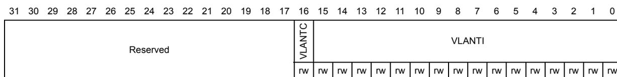
| 31 | 30 | 29 | 28 | 27 | 26 | 25 | 24 | 23 | 22 | 21 | 20 | 19 | 18 | 17 | 16 | 15 | 14 | 13 | 12 | 11 | 10 | 9 | 8 | 7 | 6 | 5 | 4 | 3 | 2 | 1 | 0 |
| Reserved | VLANTC | VLANTI | |||||||||||||||||||||||||||||
| rw | rw | rw | rw | rw | rw | rw | rw | rw | rw | rw | rw | rw | rw | rw | rw | rw | |||||||||||||||
Bits 31:17 Reserved, must be kept at reset value.
Bit 16 VLANTC : 12-bit VLAN tag comparison
When this bit is set, a 12-bit VLAN identifier, rather than the complete 16-bit VLAN tag, is used for comparison and filtering. Bits[11:0] of the VLAN tag are compared with the corresponding field in the received VLAN-tagged frame.
When this bit is reset, all 16 bits of the received VLAN frame's fifteenth and sixteenth bytes are used for comparison.
Bits 15:0 VLANTI : VLAN tag identifier (for receive frames)
This contains the 802.1Q VLAN tag to identify VLAN frames, and is compared to the fifteenth and sixteenth bytes of the frames being received for VLAN frames. Bits[15:13] are the user priority, Bit[12] is the canonical format indicator (CFI) and bits[11:0] are the VLAN tag's VLAN identifier (VID) field. When the VLANTC bit is set, only the VID (bits[11:0]) is used for comparison.
If VLANTI (VLANTI[11:0] if VLANTC is set) is all zeros, the MAC does not check the fifteenth and sixteenth bytes for VLAN tag comparison, and declares all frames with a Type field value of 0x8100 as VLAN frames.
Ethernet MAC remote wakeup frame filter register (ETH_MACRWUFR)
Address offset: 0x0028
Reset value: 0x0000 0000
This is the address through which the remote wakeup frame filter registers are written/read by the application. The Wakeup frame filter register is actually a pointer to eight (not transparent) such wakeup frame filter registers. Eight sequential write operations to this address with the offset (0x0028) will write all wakeup frame filter registers. Eight sequential read operations from this address with the offset (0x0028) will read all wakeup frame filter registers. This register contains the higher 16 bits of the 7 th MAC address. Refer to Remote wakeup frame filter register section for additional information.
Figure 360. Ethernet MAC remote wakeup frame filter register (ETH_MACRWUFR)
| Wakeup frame filter reg0 | Filter 0 Byte Mask | |||||||
| Wakeup frame filter reg1 | Filter 1 Byte Mask | |||||||
| Wakeup frame filter reg2 | Filter 2 Byte Mask | |||||||
| Wakeup frame filter reg3 | Filter 3 Byte Mask | |||||||
| Wakeup frame filter reg4 | RSVD | Filter 3 Command | RSVD | Filter 2 Command | RSVD | Filter 1 Command | RSVD | Filter 0 Command |
| Wakeup frame filter reg5 | Filter 3 Offset | Filter 2 Offset | Filter 1 Offset | Filter 0 Offset | ||||
| Wakeup frame filter reg6 | Filter 1 CRC - 16 | Filter 0 CRC - 16 | ||||||
| Wakeup frame filter reg7 | Filter 3 CRC - 16 | Filter 2 CRC - 16 | ||||||
ai15648
Ethernet MAC PMT control and status register (ETH_MACPMTCSR)
Address offset: 0x002C
Reset value: 0x0000 0000
The ETH_MACPMTCSR programs the request wakeup events and monitors the wakeup events.
| 31 | 30 | 29 | 28 | 27 | 26 | 25 | 24 | 23 | 22 | 21 | 20 | 19 | 18 | 17 | 16 | 15 | 14 | 13 | 12 | 11 | 10 | 9 | 8 | 7 | 6 | 5 | 4 | 3 | 2 | 1 | 0 |
|---|---|---|---|---|---|---|---|---|---|---|---|---|---|---|---|---|---|---|---|---|---|---|---|---|---|---|---|---|---|---|---|
| WFFRPR | Reserved | GU | Reserved | WFR | MPR | Reserved | WFE | MPE | PD | ||||||||||||||||||||||
| rs | Res. | rw | rc_r | rc_r | rw | rw | rs | ||||||||||||||||||||||||
Bit 31 WFFRPR : Wakeup frame filter register pointer reset
When set, it resets the Remote wakeup frame filter register pointer to 0b000. It is automatically cleared after 1 clock cycle.
Bits 30:10 Reserved, must be kept at reset value.
Bit 9 GU : Global unicast
When set, it enables any unicast packet filtered by the MAC (DAF) address recognition to be a wakeup frame.
Bits 8:7 Reserved, must be kept at reset value.
Bit 6 WFR : Wakeup frame received
When set, this bit indicates the power management event was generated due to reception of a wakeup frame. This bit is cleared by a read into this register.
Bit 5 MPR : Magic packet received
When set, this bit indicates the power management event was generated by the reception of a Magic Packet. This bit is cleared by a read into this register.
Bits 4:3 Reserved, must be kept at reset value.
Bit 2 WFE : Wakeup frame enable
When set, this bit enables the generation of a power management event due to wakeup frame reception.
Bit 1 MPE : Magic Packet enable
When set, this bit enables the generation of a power management event due to Magic Packet reception.
Bit 0 PD : Power down
When this bit is set, all received frames will be dropped. This bit is cleared automatically when a magic packet or wakeup frame is received, and Power-down mode is disabled. Frames received after this bit is cleared are forwarded to the application. This bit must only be set when either the Magic Packet Enable or Wakeup Frame Enable bit is set high.
Ethernet MAC interrupt status register (ETH_MACSR)
Address offset: 0x0038
Reset value: 0x0000 0000
The ETH_MACSR register contents identify the events in the MAC that can generate an interrupt.

| 15 | 14 | 13 | 12 | 11 | 10 | 9 | 8 | 7 | 6 | 5 | 4 | 3 | 2 | 1 | 0 |
|---|---|---|---|---|---|---|---|---|---|---|---|---|---|---|---|
| Reserved | TSTS | Reserved | MMCTS | MMCRS | MMCS | PMTS | Reserved | ||||||||
| rc_r | r | r | r | r | |||||||||||
Bits 15:10 Reserved, must be kept at reset value.
Bit 9 TSTS : Time stamp trigger status
This bit is set high when the system time value equals or exceeds the value specified in the Target time high and low registers. This bit is cleared by reading the ETH_PTPSSR register.
Bits 8:7 Reserved, must be kept at reset value.
Bit 6 MMCTS : MMC transmit status
This bit is set high whenever an interrupt is generated in the ETH_MMCTIR register. This bit is cleared when all the bits in this interrupt register (ETH_MMCTIR) are cleared.
Bit 5 MMCRS : MMC receive status
This bit is set high whenever an interrupt is generated in the ETH_MMCRIR register. This bit is cleared when all the bits in this interrupt register (ETH_MMCRIR) are cleared.
Bit 4 MMCS : MMC status
This bit is set high whenever any of bits 6:5 is set high. It is cleared only when both bits are low.
Bit 3 PMTS : PMT status
This bit is set whenever a Magic packet or Wake-on-LAN frame is received in Power-down mode (see bits 5 and 6 in the ETH_MACPMTCSR register Ethernet MAC PMT control and status register (ETH_MACPMTCSR) ). This bit is cleared when both bits[6:5], of this last register, are cleared due to a read operation to the ETH_MACPMTCSR register.
Bits 2:0 Reserved, must be kept at reset value.
Ethernet MAC interrupt mask register (ETH_MACIMR)
Address offset: 0x003C
Reset value: 0x0000 0000
The ETH_MACIMR register bits make it possible to mask the interrupt signal due to the corresponding event in the ETH_MACSR register.
| 15 | 14 | 13 | 12 | 11 | 10 | 9 | 8 | 7 | 6 | 5 | 4 | 3 | 2 | 1 | 0 |
|---|---|---|---|---|---|---|---|---|---|---|---|---|---|---|---|
| Reserved | TSTIM | Reserved | PMTIM | Reserved | |||||||||||
| rw | rw | ||||||||||||||
Bits 15:10 Reserved, must be kept at reset value.
Bit 9
TSTIM
: Time stamp trigger interrupt mask
When set, this bit disables the time stamp interrupt generation.
Bits 8:4 Reserved, must be kept at reset value.
Bit 3
PMTIM
: PMT interrupt mask
When set, this bit disables the assertion of the interrupt signal due to the setting of the PMT Status bit in ETH_MACSR.
Bits 2:0 Reserved, must be kept at reset value.
Ethernet MAC address 0 high register (ETH_MACA0HR)
Address offset: 0x0040
Reset value: 0x8000 FFFF
The MAC address 0 high register holds the upper 16 bits of the 6-byte first MAC address of the station. Note that the first DA byte that is received on the MII interface corresponds to the LS Byte (bits [7:0]) of the MAC address low register. For example, if 0x1122 3344 5566 is received (0x11 is the first byte) on the MII as the destination address, then the MAC address 0 register [47:0] is compared with 0x6655 4433 2211.
| 31 | 30 | 29 | 28 | 27 | 26 | 25 | 24 | 23 | 22 | 21 | 20 | 19 | 18 | 17 | 16 | 15 | 14 | 13 | 12 | 11 | 10 | 9 | 8 | 7 | 6 | 5 | 4 | 3 | 2 | 1 | 0 |
|---|---|---|---|---|---|---|---|---|---|---|---|---|---|---|---|---|---|---|---|---|---|---|---|---|---|---|---|---|---|---|---|
| MO | Reserved | MACA0H | |||||||||||||||||||||||||||||
| 1 | rw | rw | rw | rw | rw | rw | rw | rw | rw | rw | rw | rw | rw | rw | rw | rw | |||||||||||||||
Bit 31 MO : Always 1.
Bits 30:16 Reserved, must be kept at reset value.
Bits 15:0
MACA0H
: MAC address0 high [47:32]
This field contains the upper 16 bits (47:32) of the 6-byte MAC address0. This is used by the MAC for filtering for received frames and for inserting the MAC address in the transmit flow control (Pause) frames.
Ethernet MAC address 0 low register (ETH_MACA0LR)
Address offset: 0x0044
Reset value: 0xFFFF FFFF
The MAC address 0 low register holds the lower 32 bits of the 6-byte first MAC address of the station.

| 31 | 30 | 29 | 28 | 27 | 26 | 25 | 24 | 23 | 22 | 21 | 20 | 19 | 18 | 17 | 16 | 15 | 14 | 13 | 12 | 11 | 10 | 9 | 8 | 7 | 6 | 5 | 4 | 3 | 2 | 1 | 0 |
| MACA0L | |||||||||||||||||||||||||||||||
| rw | rw | rw | rw | rw | rw | rw | rw | rw | rw | rw | rw | rw | rw | rw | rw | rw | rw | rw | rw | rw | rw | rw | rw | rw | rw | rw | rw | rw | rw | rw | rw |
Bits 31:0 MACA0L : MAC address0 low [31:0]
This field contains the lower 32 bits of the 6-byte MAC address0. This is used by the MAC for filtering for received frames and for inserting the MAC address in the transmit flow control (Pause) frames.
Ethernet MAC address 1 high register (ETH_MACA1HR)
Address offset: 0x0048
Reset value: 0x0000 FFFF
The MAC address 1 high register holds the upper 16 bits of the 6-byte second MAC address of the station.

| 31 | 30 | 29 | 28 | 27 | 26 | 25 | 24 | 23 | 22 | 21 | 20 | 19 | 18 | 17 | 16 | 15 | 14 | 13 | 12 | 11 | 10 | 9 | 8 | 7 | 6 | 5 | 4 | 3 | 2 | 1 | 0 | ||
| AE | SA | MBC | Reserved | MACA1H | |||||||||||||||||||||||||||||
| rw | rw | rw | rw | rw | rw | rw | rw | rw | rw | rw | rw | rw | rw | rw | rw | rw | rw | rw | rw | rw | rw | rw | rw | rw | rw | ||||||||
Bit 31 AE : Address enable
When this bit is set, the address filters use the MAC address1 for perfect filtering. When this bit is cleared, the address filters ignore the address for filtering.
Bit 30 SA : Source address
When this bit is set, the MAC address1[47:0] is used for comparison with the SA fields of the received frame.
When this bit is cleared, the MAC address1[47:0] is used for comparison with the DA fields of the received frame.
Bits 29:24 MBC : Mask byte control
These bits are mask control bits for comparison of each of the MAC address1 bytes. When they are set high, the MAC core does not compare the corresponding byte of received DA/SA with the contents of the MAC address1 registers. Each bit controls the masking of the bytes as follows:
- – Bit 29: ETH_MACA1HR [15:8]
- – Bit 28: ETH_MACA1HR [7:0]
- – Bit 27: ETH_MACA1LR [31:24]
- – ...
- – Bit 24: ETH_MACA1LR [7:0]
Bits 23:16 Reserved, must be kept at reset value.
Bits 15:0 MACA1H : MAC address1 high [47:32]
This field contains the upper 16 bits (47:32) of the 6-byte second MAC address.
Ethernet MAC address1 low register (ETH_MACA1LR)
Address offset: 0x004C
Reset value: 0xFFFF FFFF
The MAC address 1 low register holds the lower 32 bits of the 6-byte second MAC address of the station.

| 31 | 30 | 29 | 28 | 27 | 26 | 25 | 24 | 23 | 22 | 21 | 20 | 19 | 18 | 17 | 16 | 15 | 14 | 13 | 12 | 11 | 10 | 9 | 8 | 7 | 6 | 5 | 4 | 3 | 2 | 1 | 0 |
| MACA1L | |||||||||||||||||||||||||||||||
| rw | rw | rw | rw | rw | rw | rw | rw | rw | rw | rw | rw | rw | rw | rw | rw | rw | rw | rw | rw | rw | rw | rw | rw | rw | rw | rw | rw | rw | rw | rw | rw |
Bits 31:0 MACA1L : MAC address1 low [31:0]
This field contains the lower 32 bits of the 6-byte MAC address1. The content of this field is undefined until loaded by the application after the initialization process.
Ethernet MAC address 2 high register (ETH_MACA2HR)
Address offset: 0x0050
Reset value: 0x0000 FFFF
The MAC address 2 high register holds the upper 16 bits of the 6-byte second MAC address of the station.

| 31 | 30 | 29 | 28 | 27 | 26 | 25 | 24 | 23 | 22 | 21 | 20 | 19 | 18 | 17 | 16 | 15 | 14 | 13 | 12 | 11 | 10 | 9 | 8 | 7 | 6 | 5 | 4 | 3 | 2 | 1 | 0 |
| AE | SA | MBC | Reserved | MACA2H | |||||||||||||||||||||||||||
| rw | rw | rw | rw | rw | rw | rw | rw | rw | rw | rw | rw | rw | rw | rw | rw | rw | rw | rw | rw | rw | rw | rw | rw | ||||||||
Bit 31 AE : Address enable
When this bit is set, the address filters use the MAC address2 for perfect filtering. When reset, the address filters ignore the address for filtering.
Bit 30 SA : Source address
When this bit is set, the MAC address 2 [47:0] is used for comparison with the SA fields of the received frame.
When this bit is reset, the MAC address 2 [47:0] is used for comparison with the DA fields of the received frame.
Bits 29:24 MBC : Mask byte control
These bits are mask control bits for comparison of each of the MAC address2 bytes. When set high, the MAC core does not compare the corresponding byte of received DA/SA with the contents of the MAC address 2 registers. Each bit controls the masking of the bytes as follows:
- – Bit 29: ETH_MACA2HR [15:8]
- – Bit 28: ETH_MACA2HR [7:0]
- – Bit 27: ETH_MACA2LR [31:24]
- – ...
- – Bit 24: ETH_MACA2LR [7:0]
Bits 23:16 Reserved, must be kept at reset value.
Bits 15:0 MACA2H : MAC address2 high [47:32]
This field contains the upper 16 bits (47:32) of the 6-byte MAC address2.
Ethernet MAC address 2 low register (ETH_MACA2LR)
Address offset: 0x0054
Reset value: 0xFFFF FFFF
The MAC address 2 low register holds the lower 32 bits of the 6-byte second MAC address of the station.

| 31 | 30 | 29 | 28 | 27 | 26 | 25 | 24 | 23 | 22 | 21 | 20 | 19 | 18 | 17 | 16 | 15 | 14 | 13 | 12 | 11 | 10 | 9 | 8 | 7 | 6 | 5 | 4 | 3 | 2 | 1 | 0 |
| MACA2L | |||||||||||||||||||||||||||||||
| rw | rw | rw | rw | rw | rw | rw | rw | rw | rw | rw | rw | rw | rw | rw | rw | rw | rw | rw | rw | rw | rw | rw | rw | rw | rw | rw | rw | rw | rw | rw | rw |
Bits 31:0 MACA2L : MAC address2 low [31:0]
This field contains the lower 32 bits of the 6-byte second MAC address2. The content of this field is undefined until loaded by the application after the initialization process.
Ethernet MAC address 3 high register (ETH_MACA3HR)Address offset: 0x0058
Reset value: 0x0000 FFFF
The MAC address 3 high register holds the upper 16 bits of the 6-byte second MAC address of the station.

| 31 | 30 | 29 | 28 | 27 | 26 | 25 | 24 | 23 | 22 | 21 | 20 | 19 | 18 | 17 | 16 | 15 | 14 | 13 | 12 | 11 | 10 | 9 | 8 | 7 | 6 | 5 | 4 | 3 | 2 | 1 | 0 |
| AE | SA | MBC | Reserved | MACA3H | |||||||||||||||||||||||||||
| rw | rw | rw | rw | rw | rw | rw | rw | rw | rw | rw | rw | rw | rw | rw | rw | rw | rw | rw | rw | rw | rw | rw | rw | ||||||||
Bit 31 AE : Address enable
When this bit is set, the address filters use the MAC address3 for perfect filtering. When this bit is cleared, the address filters ignore the address for filtering.
Bit 30 SA : Source address
When this bit is set, the MAC address 3 [47:0] is used for comparison with the SA fields of the received frame.
When this bit is cleared, the MAC address 3[47:0] is used for comparison with the DA fields of the received frame.
Bits 29:24 MBC : Mask byte control
These bits are mask control bits for comparison of each of the MAC address3 bytes. When these bits are set high, the MAC core does not compare the corresponding byte of received DA/SA with the contents of the MAC address 3 registers. Each bit controls the masking of the bytes as follows:
- – Bit 29: ETH_MACA3HR [15:8]
- – Bit 28: ETH_MACA3HR [7:0]
- – Bit 27: ETH_MACA3LR [31:24]
- ...
- – Bit 24: ETH_MACA3LR [7:0]
Bits 23:16 Reserved, must be kept at reset value.
Bits 15:0 MACA3H : MAC address3 high [47:32]
This field contains the upper 16 bits (47:32) of the 6-byte MAC address3.
Ethernet MAC address 3 low register (ETH_MACA3LR)Address offset: 0x005C
Reset value: 0xFFFF FFFF
The MAC address 3 low register holds the lower 32 bits of the 6-byte second MAC address of the station.

| 31 | 30 | 29 | 28 | 27 | 26 | 25 | 24 | 23 | 22 | 21 | 20 | 19 | 18 | 17 | 16 | 15 | 14 | 13 | 12 | 11 | 10 | 9 | 8 | 7 | 6 | 5 | 4 | 3 | 2 | 1 | 0 |
| MACA3L | |||||||||||||||||||||||||||||||
| rw | rw | rw | rw | rw | rw | rw | rw | rw | rw | rw | rw | rw | rw | rw | rw | rw | rw | rw | rw | rw | rw | rw | rw | rw | rw | rw | rw | rw | rw | rw | rw |
Bits 31:0 MACA3L : MAC address3 low [31:0]
This field contains the lower 32 bits of the 6-byte second MAC address3. The content of this field is undefined until loaded by the application after the initialization process.
29.8.2 MMC register description
Ethernet MMC control register (ETH_MMCCR)
Address offset: 0x0100
Reset value: 0x0000 0000
The Ethernet MMC Control register establishes the operating mode of the management counters.

| 31 | 30 | 29 | 28 | 27 | 26 | 25 | 24 | 23 | 22 | 21 | 20 | 19 | 18 | 17 | 16 | 15 | 14 | 13 | 12 | 11 | 10 | 9 | 8 | 7 | 6 | 5 | 4 | 3 | 2 | 1 | 0 |
| Reserved | MCF | ROR | CSR | CR | |||||||||||||||||||||||||||
| rw | rw | rw | rw | ||||||||||||||||||||||||||||
Bits 31:4 Reserved, must be kept at reset value.
Bit 3 MCF : MMC counter freeze
When set, this bit freezes all the MMC counters to their current value. (None of the MMC counters are updated due to any transmitted or received frame until this bit is cleared to 0. If any MMC counter is read with the Reset on Read bit set, then that counter is also cleared in this mode.)
Bit 2 ROR : Reset on read
When this bit is set, the MMC counters is reset to zero after read (self-clearing after reset). The counters are cleared when the least significant byte lane (bits [7:0]) is read.
Bit 1 CSR : Counter stop rollover
When this bit is set, the counter does not roll over to zero after it reaches the maximum value.
Bit 0 CR : Counter reset
When it is set, all counters are reset. This bit is cleared automatically after 1 clock cycle.
Ethernet MMC receive interrupt register (ETH_MMCRIR)
Address offset: 0x0104
Reset value: 0x0000 0000
The Ethernet MMC receive interrupt register maintains the interrupts generated when receive statistic counters reach half their maximum values. (MSB of the counter is set.) It is a 32-bit wide register. An interrupt bit is cleared when the respective MMC counter that caused the interrupt is read. The least significant byte lane (bits [7:0]) of the respective counter must be read in order to clear the interrupt bit.
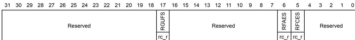
| 31 | 30 | 29 | 28 | 27 | 26 | 25 | 24 | 23 | 22 | 21 | 20 | 19 | 18 | 17 | 16 | 15 | 14 | 13 | 12 | 11 | 10 | 9 | 8 | 7 | 6 | 5 | 4 | 3 | 2 | 1 | 0 |
| Reserved | RGUFS | Reserved | RFAES | RFCES | Reserved | ||||||||||||||||||||||||||
| rc_r | rc_r | rc_r | |||||||||||||||||||||||||||||
Bits 31:18 Reserved, must be kept at reset value.
Bit 17 RGUFS : Received Good Unicast Frames Status
This bit is set when the received, good unicast frames, counter reaches half the maximum value.
Bits 16:7 Reserved, must be kept at reset value.
Bit 6 RFAES : Received frames alignment error status
This bit is set when the received frames, with alignment error, counter reaches half the maximum value.
Bit 5 RFCES : Received frames CRC error status
This bit is set when the received frames, with CRC error, counter reaches half the maximum value.
Bits 4:0 Reserved, must be kept at reset value.
Ethernet MMC transmit interrupt register (ETH_MMCTIR)
Address offset: 0x0108
Reset value: 0x0000 0000
The Ethernet MMC transmit Interrupt register maintains the interrupts generated when transmit statistic counters reach half their maximum values. (MSB of the counter is set.) It is a 32-bit wide register. An interrupt bit is cleared when the respective MMC counter that caused the interrupt is read. The least significant byte lane (bits [7:0]) of the respective counter must be read in order to clear the interrupt bit.
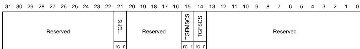
| 31 | 30 | 29 | 28 | 27 | 26 | 25 | 24 | 23 | 22 | 21 | 20 | 19 | 18 | 17 | 16 | 15 | 14 | 13 | 12 | 11 | 10 | 9 | 8 | 7 | 6 | 5 | 4 | 3 | 2 | 1 | 0 |
|---|---|---|---|---|---|---|---|---|---|---|---|---|---|---|---|---|---|---|---|---|---|---|---|---|---|---|---|---|---|---|---|
| Reserved | TGFS | Reserved | TGFMSCS | TGFSCS | Reserved | ||||||||||||||||||||||||||
| rc_r | rc_r | rc_r | |||||||||||||||||||||||||||||
Bits 31:22 Reserved, must be kept at reset value.
Bit 21 TGFS : Transmitted good frames status
This bit is set when the transmitted, good frames, counter reaches half the maximum value.
Bits 20:16 Reserved, must be kept at reset value.
Bit 15 TGFMSCS : Transmitted good frames more single collision status
This bit is set when the transmitted, good frames after more than a single collision, counter reaches half the maximum value.
Bit 14 TGFSCS : Transmitted good frames single collision status
This bit is set when the transmitted, good frames after a single collision, counter reaches half the maximum value.
Bits 13:0 Reserved, must be kept at reset value.
Ethernet MMC receive interrupt mask register (ETH_MMCRIMR)
Address offset: 0x010C
Reset value: 0x0000 0000
The Ethernet MMC receive interrupt mask register maintains the masks for interrupts generated when the receive statistic counters reach half their maximum value. (MSB of the counter is set.) It is a 32-bit wide register.
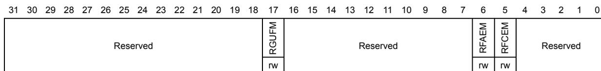
| 31 | 30 | 29 | 28 | 27 | 26 | 25 | 24 | 23 | 22 | 21 | 20 | 19 | 18 | 17 | 16 | 15 | 14 | 13 | 12 | 11 | 10 | 9 | 8 | 7 | 6 | 5 | 4 | 3 | 2 | 1 | 0 |
| Reserved | RGUFM | Reserved | RFAEM | RFCEM | Reserved | ||||||||||||||||||||||||||
| rw | rw | rw | |||||||||||||||||||||||||||||
Bits 31:18 Reserved, must be kept at reset value.
Bit 17 RGUFM : Received good unicast frames mask
Setting this bit masks the interrupt when the received, good unicast frames, counter reaches half the maximum value.
Bits 16:7 Reserved, must be kept at reset value.
Bit 6 RFAEM : Received frames alignment error mask
Setting this bit masks the interrupt when the received frames, with alignment error, counter reaches half the maximum value.
Bit 5 RFCEM : Received frame CRC error mask
Setting this bit masks the interrupt when the received frames, with CRC error, counter reaches half the maximum value.
Bits 4:0 Reserved, must be kept at reset value.
Ethernet MMC transmit interrupt mask register (ETH_MMCTIMR)
Address offset: 0x0110
Reset value: 0x0000 0000
The Ethernet MMC transmit interrupt mask register maintains the masks for interrupts generated when the transmit statistic counters reach half their maximum value. (MSB of the counter is set.) It is a 32-bit wide register.
| 31 | 30 | 29 | 28 | 27 | 26 | 25 | 24 | 23 | 22 | 21 | 20 | 19 | 18 | 17 | 16 | 15 | 14 | 13 | 12 | 11 | 10 | 9 | 8 | 7 | 6 | 5 | 4 | 3 | 2 | 1 | 0 |
| Reserved | TGFM | Reserved | TGFMSCM | TGFSCM | Reserved | ||||||||||||||||||||||||||
| rw | rw | rw | |||||||||||||||||||||||||||||
Bits 31:22 Reserved, must be kept at reset value.
Bit 21 TGFM : Transmitted good frames mask
Setting this bit masks the interrupt when the transmitted, good frames, counter reaches half the maximum value.
Bits 20:16 Reserved, must be kept at reset value.
Bit 15 TGFMSMCM : Transmitted good frames more single collision mask
Setting this bit masks the interrupt when the transmitted good frames after more than a single collision counter reaches half the maximum value.
Bit 14 TGFSCM : Transmitted good frames single collision mask
Setting this bit masks the interrupt when the transmitted good frames after a single collision counter reaches half the maximum value.
Bits 13:0 Reserved, must be kept at reset value.
Ethernet MMC transmitted good frames after a single collision counter register (ETH_MMCTGFSCCR)
Address offset: 0x014C
Reset value: 0x0000 0000
This register contains the number of successfully transmitted frames after a single collision in Half-duplex mode.

| 31 | 30 | 29 | 28 | 27 | 26 | 25 | 24 | 23 | 22 | 21 | 20 | 19 | 18 | 17 | 16 | 15 | 14 | 13 | 12 | 11 | 10 | 9 | 8 | 7 | 6 | 5 | 4 | 3 | 2 | 1 | 0 |
| TGFSCC | |||||||||||||||||||||||||||||||
| r | r | r | r | r | r | r | r | r | r | r | r | r | r | r | r | r | r | r | r | r | r | r | r | r | r | r | r | r | r | r | r |
Bits 31:0 TGFSCC : Transmitted good frames single collision counter
Transmitted good frames after a single collision counter.
Ethernet MMC transmitted good frames after more than a single collision counter register (ETH_MMCTGFMSCCR)
Address offset: 0x0150
Reset value: 0x0000 0000
This register contains the number of successfully transmitted frames after more than a single collision in Half-duplex mode.

| 31 | 30 | 29 | 28 | 27 | 26 | 25 | 24 | 23 | 22 | 21 | 20 | 19 | 18 | 17 | 16 | 15 | 14 | 13 | 12 | 11 | 10 | 9 | 8 | 7 | 6 | 5 | 4 | 3 | 2 | 1 | 0 |
| TGFMSCC | |||||||||||||||||||||||||||||||
| r | r | r | r | r | r | r | r | r | r | r | r | r | r | r | r | r | r | r | r | r | r | r | r | r | r | r | r | r | r | r | r |
Bits 31:0 TGFMSCC : Transmitted good frames more single collision counter
Transmitted good frames after more than a single collision counter
Ethernet MMC transmitted good frames counter register (ETH_MMCTGFCR)
Address offset: 0x0168
Reset value: 0x0000 0000
This register contains the number of good frames transmitted.

| 31 | 30 | 29 | 28 | 27 | 26 | 25 | 24 | 23 | 22 | 21 | 20 | 19 | 18 | 17 | 16 | 15 | 14 | 13 | 12 | 11 | 10 | 9 | 8 | 7 | 6 | 5 | 4 | 3 | 2 | 1 | 0 | |
| TGFC | ||||||||||||||||||||||||||||||||
| r | r | r | r | r | r | r | r | r | r | r | r | r | r | r | r | r | r | r | r | r | r | r | r | r | r | r | r | r | r | r | r | r |
Bits 31:0 TGFC : Transmitted good frames counter
Ethernet MMC received frames with CRC error counter register (ETH_MMCRFCECR)
Address offset: 0x0194
Reset value: 0x0000 0000
This register contains the number of frames received with CRC error.

| 31 | 30 | 29 | 28 | 27 | 26 | 25 | 24 | 23 | 22 | 21 | 20 | 19 | 18 | 17 | 16 | 15 | 14 | 13 | 12 | 11 | 10 | 9 | 8 | 7 | 6 | 5 | 4 | 3 | 2 | 1 | 0 | |
| RFCEC | ||||||||||||||||||||||||||||||||
| r | r | r | r | r | r | r | r | r | r | r | r | r | r | r | r | r | r | r | r | r | r | r | r | r | r | r | r | r | r | r | r | r |
Bits 31:0
RFCEC
: Received frames CRC error counter
Received frames with CRC error counter
Ethernet MMC received frames with alignment error counter register (ETH_MMCRFAECR)
Address offset: 0x0198
Reset value: 0x0000 0000
This register contains the number of frames received with alignment (dribble) error.

| 31 | 30 | 29 | 28 | 27 | 26 | 25 | 24 | 23 | 22 | 21 | 20 | 19 | 18 | 17 | 16 | 15 | 14 | 13 | 12 | 11 | 10 | 9 | 8 | 7 | 6 | 5 | 4 | 3 | 2 | 1 | 0 | |
| RFAEC | ||||||||||||||||||||||||||||||||
| r | r | r | r | r | r | r | r | r | r | r | r | r | r | r | r | r | r | r | r | r | r | r | r | r | r | r | r | r | r | r | r | r |
Bits 31:0
RFAEC
: Received frames alignment error counter
Received frames with alignment error counter
MMC received good unicast frames counter register (ETH_MMCRGUFCR)
Address offset: 0x01C4
Reset value: 0x0000 0000
This register contains the number of good unicast frames received.

| 31 | 30 | 29 | 28 | 27 | 26 | 25 | 24 | 23 | 22 | 21 | 20 | 19 | 18 | 17 | 16 | 15 | 14 | 13 | 12 | 11 | 10 | 9 | 8 | 7 | 6 | 5 | 4 | 3 | 2 | 1 | 0 | |
| RGUFC | ||||||||||||||||||||||||||||||||
| r | r | r | r | r | r | r | r | r | r | r | r | r | r | r | r | r | r | r | r | r | r | r | r | r | r | r | r | r | r | r | r | r |
Bits 31:0 RGUFC : Received good unicast frames counter
29.8.3 IEEE 1588 time stamp registers
This section describes the registers required to support precision network clock synchronization functions under the IEEE 1588 standard.
Ethernet PTP time stamp control register (ETH_PTPSCR)
Address offset: 0x0700
Reset value: 0x0000 0000
This register controls the time stamp generation and update logic.
| 31 | 30 | 29 | 28 | 27 | 26 | 25 | 24 | 23 | 22 | 21 | 20 | 19 | 18 | 17 | 16 | 15 | 14 | 13 | 12 | 11 | 10 | 9 | 8 | 7 | 6 | 5 | 4 | 3 | 2 | 1 | 0 |
| Reserved | TSARU | TSITE | TSSTU | TSSTI | TSFCU | TSE | |||||||||||||||||||||||||
| rw | rw | rw | rw | rw | rw | ||||||||||||||||||||||||||
Bits 31:6 Reserved, must be kept at reset value.
Bit 5 TSARU : Time stamp addend register update
When this bit is set, the Time stamp addend register's contents are updated to the PTP block for fine correction. This bit is cleared when the update is completed. This register bit must be read as zero before you can set it.
Bit 4 TSITE : Time stamp interrupt trigger enable
When this bit is set, a time stamp interrupt is generated when the system time becomes greater than the value written in Target Time register. When the Time Stamp Trigger interrupt is generated, this bit is cleared.
Bit 3 TSSTU : Time stamp system time update
When this bit is set, the system time is updated (added to or subtracted from) with the value specified in the Time stamp high update and Time stamp low update registers. Both the TSSTU and TSSTI bits must be read as zero before you can set this bit. Once the update is completed in hardware, this bit is cleared.
Bit 2 TSSTI : Time stamp system time initialize
When this bit is set, the system time is initialized (overwritten) with the value specified in the Time stamp high update and Time stamp low update registers. This bit must be read as zero before you can set it. When initialization is complete, this bit is cleared.
Bit 1 TSFCU : Time stamp fine or coarse update
When set, this bit indicates that the system time stamp is to be updated using the Fine Update method. When cleared, it indicates the system time stamp is to be updated using the Coarse method.
Bit 0 TSE : Time stamp enable
When this bit is set, time stamping is enabled for transmit and receive frames. When this bit is cleared, the time stamp function is suspended and time stamps are not added for transmit and receive frames. Because the maintained system time is suspended, you must always initialize the time stamp feature (system time) after setting this bit high.
Ethernet PTP subsecond increment register (ETH_PTPSSIR)
Address offset: 0x0704
Reset value: 0x0000 0000
This register contains the 8-bit value by which the subsecond register is incremented. In Coarse update mode (TSFCU bit in ETH_PTPTSCR), the value in this register is added to the system time every clock cycle of HCLK. In Fine update mode, the value in this register is added to the system time whenever the accumulator gets an overflow.

| 31 | 30 | 29 | 28 | 27 | 26 | 25 | 24 | 23 | 22 | 21 | 20 | 19 | 18 | 17 | 16 | 15 | 14 | 13 | 12 | 11 | 10 | 9 | 8 | 7 | 6 | 5 | 4 | 3 | 2 | 1 | 0 |
| Reserved | STSSI | ||||||||||||||||||||||||||||||
| rw | rw | rw | rw | rw | rw | rw | rw | ||||||||||||||||||||||||
Bits 31:8 Reserved, must be kept at reset value.
Bits 7:0 STSSI : System time subsecond increment
The value programmed in this register is added to the contents of the subsecond value of the system time in every update.
For example, to achieve 20 ns accuracy, the value is: \( 20 / 0.467 \approx 43 \) (or 0x2A).
Ethernet PTP time stamp high register (ETH_PTPTSHR)
Address offset: 0x0708
Reset value: 0x0000 0000
This register contains the most significant (higher) 32 time bits. This read-only register contains the seconds system time value. The Time stamp high register, along with Time stamp low register, indicates the current value of the system time maintained by the MAC. Though it is updated on a continuous basis.

| 31 | 30 | 29 | 28 | 27 | 26 | 25 | 24 | 23 | 22 | 21 | 20 | 19 | 18 | 17 | 16 | 15 | 14 | 13 | 12 | 11 | 10 | 9 | 8 | 7 | 6 | 5 | 4 | 3 | 2 | 1 | 0 |
| STS | |||||||||||||||||||||||||||||||
| r | r | r | r | r | r | r | r | r | r | r | r | r | r | r | r | r | r | r | r | r | r | r | r | r | r | r | r | r | r | r | r |
Bits 31:0 STS : System time second
The value in this field indicates the current value in seconds of the System Time maintained by the core.
Ethernet PTP time stamp low register (ETH_PTPTSLR)Address offset: 0x070C
Reset value: 0x0000 0000
This register contains the least significant (lower) 32 time bits. This read-only register contains the subsecond system time value.
| 31 | 30 | 29 | 28 | 27 | 26 | 25 | 24 | 23 | 22 | 21 | 20 | 19 | 18 | 17 | 16 | 15 | 14 | 13 | 12 | 11 | 10 | 9 | 8 | 7 | 6 | 5 | 4 | 3 | 2 | 1 | 0 |
| STPNS | STSS | ||||||||||||||||||||||||||||||
| r | r | r | r | r | r | r | r | r | r | r | r | r | r | r | r | r | r | r | r | r | r | r | r | r | r | r | r | r | r | r | r |
Bit 31 STPNS : System time positive or negative sign
This bit indicates a positive or negative time value. When set, the bit indicates that time representation is negative. When cleared, it indicates that time representation is positive. Because the system time should always be positive, this bit is normally zero.
Bits 30:0 STSS : System time subseconds
The value in this field has the subsecond time representation, with 0.46 ns accuracy.
Ethernet PTP time stamp high update register (ETH_PTPTSHUR)Address offset: 0x0710
Reset value: 0x0000 0000
This register contains the most significant (higher) 32 bits of the time to be written to, added to, or subtracted from the System Time value. The Time stamp high update register, along with the Time stamp update low register, initializes or updates the system time maintained by the MAC. You have to write both of these registers before setting the TSSTI or TSSTU bits in the Time stamp control register.

| 31 | 30 | 29 | 28 | 27 | 26 | 25 | 24 | 23 | 22 | 21 | 20 | 19 | 18 | 17 | 16 | 15 | 14 | 13 | 12 | 11 | 10 | 9 | 8 | 7 | 6 | 5 | 4 | 3 | 2 | 1 | 0 |
| TSUS | |||||||||||||||||||||||||||||||
| rw | rw | rw | rw | rw | rw | rw | rw | rw | rw | rw | rw | rw | rw | rw | rw | rw | rw | rw | rw | rw | rw | rw | rw | rw | rw | rw | rw | rw | rw | rw | rw |
Bits 31:0 TSUS : Time stamp update second
The value in this field indicates the time, in seconds, to be initialized or added to the system time.
Ethernet PTP time stamp low update register (ETH_PTPTSLUR)
Address offset: 0x0714
Reset value: 0x0000 0000
This register contains the least significant (lower) 32 bits of the time to be written to, added to, or subtracted from the System Time value.
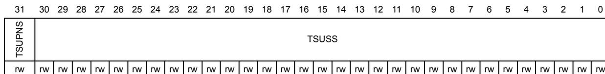
| 31 | 30 | 29 | 28 | 27 | 26 | 25 | 24 | 23 | 22 | 21 | 20 | 19 | 18 | 17 | 16 | 15 | 14 | 13 | 12 | 11 | 10 | 9 | 8 | 7 | 6 | 5 | 4 | 3 | 2 | 1 | 0 |
| TSUPNS | TSUSS | ||||||||||||||||||||||||||||||
| rw | rw | rw | rw | rw | rw | rw | rw | rw | rw | rw | rw | rw | rw | rw | rw | rw | rw | rw | rw | rw | rw | rw | rw | rw | rw | rw | rw | rw | rw | rw | rw |
Bit 31 TSUPNS : Time stamp update positive or negative sign
This bit indicates positive or negative time value. When set, the bit indicates that time representation is negative. When cleared, it indicates that time representation is positive. When TSSTI is set (system time initialization) this bit should be zero. If this bit is set when TSSTU is set, the value in the Time stamp update registers is subtracted from the system time. Otherwise it is added to the system time.
Bits 30:0 TSUSS : Time stamp update subseconds
The value in this field indicates the subsecond time to be initialized or added to the system time. This value has an accuracy of 0.46 ns (in other words, a value of 0x0000_0001 is 0.46 ns).
Ethernet PTP time stamp addend register (ETH_PTPTSAR)
Address offset: 0x0718
Reset value: 0x0000 0000
This register is used by the software to readjust the clock frequency linearly to match the master clock frequency. This register value is used only when the system time is configured for Fine update mode (TSFCU bit in ETH_PTPTSCR). This register content is added to a 32-bit accumulator in every clock cycle and the system time is updated whenever the accumulator overflows.

| 31 | 30 | 29 | 28 | 27 | 26 | 25 | 24 | 23 | 22 | 21 | 20 | 19 | 18 | 17 | 16 | 15 | 14 | 13 | 12 | 11 | 10 | 9 | 8 | 7 | 6 | 5 | 4 | 3 | 2 | 1 | 0 |
| TSA | |||||||||||||||||||||||||||||||
| rw | rw | rw | rw | rw | rw | rw | rw | rw | rw | rw | rw | rw | rw | rw | rw | rw | rw | rw | rw | rw | rw | rw | rw | rw | rw | rw | rw | rw | rw | rw | rw |
Bits 31:0 TSA : Time stamp addend
This register indicates the 32-bit time value to be added to the Accumulator register to achieve time synchronization.
Ethernet PTP target time high register (ETH_PTPTTHR)
Address offset: 0x071C
Reset value: 0x0000 0000
This register contains the higher 32 bits of time to be compared with the system time for interrupt event generation. The Target time high register, along with Target time low register, is used to schedule an interrupt event (TSARU bit in ETH_PTPTSCR) when the system time exceeds the value programmed in these registers.
| 31 | 30 | 29 | 28 | 27 | 26 | 25 | 24 | 23 | 22 | 21 | 20 | 19 | 18 | 17 | 16 | 15 | 14 | 13 | 12 | 11 | 10 | 9 | 8 | 7 | 6 | 5 | 4 | 3 | 2 | 1 | 0 |
|---|---|---|---|---|---|---|---|---|---|---|---|---|---|---|---|---|---|---|---|---|---|---|---|---|---|---|---|---|---|---|---|
| TTSH | |||||||||||||||||||||||||||||||
| rw | rw | rw | rw | rw | rw | rw | rw | rw | rw | rw | rw | rw | rw | rw | rw | rw | rw | rw | rw | rw | rw | rw | rw | rw | rw | rw | rw | rw | rw | rw | rw |
Bits 31:0 TTSH : Target time stamp high
This register stores the time in seconds. When the time stamp value matches or exceeds both Target time stamp registers, the MAC, if enabled, generates an interrupt.
Ethernet PTP target time low register (ETH_PTPTTLR)
Address offset: 0x0720
Reset value: 0x0000 0000
This register contains the lower 32 bits of time to be compared with the system time for interrupt event generation.
| 31 | 30 | 29 | 28 | 27 | 26 | 25 | 24 | 23 | 22 | 21 | 20 | 19 | 18 | 17 | 16 | 15 | 14 | 13 | 12 | 11 | 10 | 9 | 8 | 7 | 6 | 5 | 4 | 3 | 2 | 1 | 0 |
|---|---|---|---|---|---|---|---|---|---|---|---|---|---|---|---|---|---|---|---|---|---|---|---|---|---|---|---|---|---|---|---|
| TTSL | |||||||||||||||||||||||||||||||
| rw | rw | rw | rw | rw | rw | rw | rw | rw | rw | rw | rw | rw | rw | rw | rw | rw | rw | rw | rw | rw | rw | rw | rw | rw | rw | rw | rw | rw | rw | rw | rw |
Bits 31:0 TTSL : Target time stamp low
This register stores the time in (signed) nanoseconds. When the value of the time stamp matches or exceeds both Target time stamp registers, the MAC, if enabled, generates an interrupt.
29.8.4 DMA register description
This section defines the bits for each DMA register. Non-32 bit accesses are allowed as long as the address is word-aligned.
Ethernet DMA bus mode register (ETH_DMABMR)
Address offset: 0x1000
Reset value: 0x0002 0101
The bus mode register establishes the bus operating modes for the DMA.
| 31 | 30 | 29 | 28 | 27 | 26 | 25 | 24 | 23 | 22 | 21 | 20 | 19 | 18 | 17 | 16 | 15 | 14 | 13 | 12 | 11 | 10 | 9 | 8 | 7 | 6 | 5 | 4 | 3 | 2 | 1 | 0 |
|---|---|---|---|---|---|---|---|---|---|---|---|---|---|---|---|---|---|---|---|---|---|---|---|---|---|---|---|---|---|---|---|
| Reserved | AAB | FPM | USP | RDP | FB | PM | PBL | Reserved | DSL | DA | SR | ||||||||||||||||||||
| rw | rw | rw | rw | rw | rw | rw | rw | rw | rw | rw | rw | rw | rw | rw | rw | rw | rw | rw | rw | rw | rw | rw | rw | rs | |||||||
Bits 31:26 Reserved, must be kept at reset value.
Bit 25 AAB : Address-aligned beats
When this bit is set high and the FB bit equals 1, the AHB interface generates all bursts aligned to the start address LS bits. If the FB bit equals 0, the first burst (accessing the data buffer's start address) is not aligned, but subsequent bursts are aligned to the address.
Bit 24 FPM : 4xPBL mode
When set high, this bit multiplies the PBL value programmed (bits [22:17] and bits [13:8]) four times. Thus the DMA transfers data in a maximum of 4, 8, 16, 32, 64 and 128 beats depending on the PBL value.
Bit 23 USP : Use separate PBL
When set high, it configures the RxDMA to use the value configured in bits [22:17] as PBL while the PBL value in bits [13:8] is applicable to TxDMA operations only. When this bit is cleared, the PBL value in bits [13:8] is applicable for both DMA engines.
Bits 22:17 RDP : Rx DMA PBL
These bits indicate the maximum number of beats to be transferred in one RxDMA transaction. This is the maximum value that is used in a single block read/write operation. The RxDMA always attempts to burst as specified in RDP each time it starts a burst transfer on the host bus. RDP can be programmed with permissible values of 1, 2, 4, 8, 16, and 32. Any other value results in undefined behavior.
These bits are valid and applicable only when USP is set high.
Bit 16 FB : Fixed burst
This bit controls whether the AHB Master interface performs fixed burst transfers or not. When set, the AHB uses only SINGLE, INCR4, INCR8 or INCR16 during start of normal burst transfers. When reset, the AHB uses SINGLE and INCR burst transfer operations.
Bits 15:14 PM : Rx Tx priority ratio
RxDMA requests are given priority over TxDMA requests in the following ratio:
00: 1:1
01: 2:1
10: 3:1
11: 4:1
This is valid only when the DA bit is cleared.
Bits 13:8 PBL : Programmable burst length
These bits indicate the maximum number of beats to be transferred in one DMA transaction. This is the maximum value that is used in a single block read/write operation. The DMA always attempts to burst as specified in PBL each time it starts a burst transfer on the host bus. PBL can be programmed with permissible values of 1, 2, 4, 8, 16, and 32. Any other value results in undefined behavior. When USP is set, this PBL value is applicable for TxDMA transactions only.
The PBL values have the following limitations:
- – The maximum number of beats (PBL) possible is limited by the size of the Tx FIFO and Rx FIFO.
- – The FIFO has a constraint that the maximum beat supported is half the depth of the FIFO.
- – If the PBL is common for both transmit and receive DMA, the minimum Rx FIFO and Tx FIFO depths must be considered.
- – Do not program out-of-range PBL values, because the system may not behave properly.
Bit 7 Reserved, must be kept at reset value.
Bits 6:2 DSL : Descriptor skip length
This bit specifies the number of words to skip between two unchained descriptors. The address skipping starts from the end of current descriptor to the start of next descriptor. When DSL value equals zero, the descriptor table is taken as contiguous by the DMA, in Ring mode.
Bit 1 DA : DMA Arbitration
0: Round-robin with Rx:TxD priority given in bits [15:14]
1: Rx has priority over Tx
Bit 0 SR : Software reset
When this bit is set, the MAC DMA controller resets all MAC Subsystem internal registers and logic. It is cleared automatically after the reset operation has completed in all of the core clock domains. Read a 0 value in this bit before re-programming any register of the core.
Ethernet DMA transmit poll demand register (ETH_DMATPDR)
Address offset: 0x1004
Reset value: 0x0000 0000
This register is used by the application to instruct the DMA to poll the transmit descriptor list. The transmit poll demand register enables the Transmit DMA to check whether or not the current descriptor is owned by DMA. The Transmit Poll Demand command is given to wake up the TxDMA if it is in Suspend mode. The TxDMA can go into Suspend mode due to an underflow error in a transmitted frame or due to the unavailability of descriptors owned by transmit DMA. You can issue this command anytime and the TxDMA resets it once it starts re-fetching the current descriptor from host memory.

| 31 | 30 | 29 | 28 | 27 | 26 | 25 | 24 | 23 | 22 | 21 | 20 | 19 | 18 | 17 | 16 | 15 | 14 | 13 | 12 | 11 | 10 | 9 | 8 | 7 | 6 | 5 | 4 | 3 | 2 | 1 | 0 |
| TPD | |||||||||||||||||||||||||||||||
| rw_wt | |||||||||||||||||||||||||||||||
Bits 31:0 TPD: Transmit poll demand
When these bits are written with any value, the DMA reads the current descriptor pointed to by the ETH_DMACHTDR register. If that descriptor is not available (owned by Host), transmission returns to the Suspend state and ETH_DMASR register bit 2 is asserted. If the descriptor is available, transmission resumes.
EHERNET DMA receive poll demand register (ETH_DMARPDR)
Address offset: 0x1008
Reset value: 0x0000 0000
This register is used by the application to instruct the DMA to poll the receive descriptor list. The Receive poll demand register enables the receive DMA to check for new descriptors. This command is given to wake up the RxDMA from Suspend state. The RxDMA can go into Suspend state only due to the unavailability of descriptors owned by it.

| 31 | 30 | 29 | 28 | 27 | 26 | 25 | 24 | 23 | 22 | 21 | 20 | 19 | 18 | 17 | 16 | 15 | 14 | 13 | 12 | 11 | 10 | 9 | 8 | 7 | 6 | 5 | 4 | 3 | 2 | 1 | 0 |
| RPD | |||||||||||||||||||||||||||||||
| rw_wt | |||||||||||||||||||||||||||||||
Bits 31:0 RPD : Receive poll demand
When these bits are written with any value, the DMA reads the current descriptor pointed to by the ETH_DMACHRDR register. If that descriptor is not available (owned by Host), reception returns to the Suspended state and ETH_DMASR register bit 7 is not asserted. If the descriptor is available, the Receive DMA returns to active state.
Ethernet DMA receive descriptor list address register (ETH_DMARDLAR)
Address offset: 0x100C
Reset value: 0x0000 0000
The Receive descriptor list address register points to the start of the receive descriptor list. The descriptor lists reside in the STM32F107xx's physical memory space and must be word-aligned. The DMA internally converts it to bus-width aligned address by making the corresponding LS bits low. Writing to the ETH_DMARDLAR register is permitted only when reception is stopped. When stopped, the ETH_DMARDLAR register must be written to before the receive Start command is given.

| 31 | 30 | 29 | 28 | 27 | 26 | 25 | 24 | 23 | 22 | 21 | 20 | 19 | 18 | 17 | 16 | 15 | 14 | 13 | 12 | 11 | 10 | 9 | 8 | 7 | 6 | 5 | 4 | 3 | 2 | 1 | 0 |
| SRL | |||||||||||||||||||||||||||||||
| rw | rw | rw | rw | rw | rw | rw | rw | rw | rw | rw | rw | rw | rw | rw | rw | rw | rw | rw | rw | rw | rw | rw | rw | rw | rw | rw | rw | rw | rw | rw | rw |
Bits 31:0 SRL : Start of receive list
This field contains the base address of the first descriptor in the receive descriptor list. The LSB bits [1/2/3:0] for 32/64/128-bit bus width) are internally ignored and taken as all-zero by the DMA. Hence these LSB bits are read only.
Ethernet DMA transmit descriptor list address register (ETH_DMATDLAR)
Address offset: 0x1010
Reset value: 0x0000 0000
The Transmit descriptor list address register points to the start of the transmit descriptor list. The descriptor lists reside in the STM32F107xx's physical memory space and must be word-aligned. The DMA internally converts it to bus-width-aligned address by taking the corresponding LSB to low. Writing to the ETH_DMATDLAR register is permitted only when transmission has stopped. Once transmission has stopped, the ETH_DMATDLAR register can be written before the transmission Start command is given.

| 31 | 30 | 29 | 28 | 27 | 26 | 25 | 24 | 23 | 22 | 21 | 20 | 19 | 18 | 17 | 16 | 15 | 14 | 13 | 12 | 11 | 10 | 9 | 8 | 7 | 6 | 5 | 4 | 3 | 2 | 1 | 0 |
| STL | |||||||||||||||||||||||||||||||
| rw | rw | rw | rw | rw | rw | rw | rw | rw | rw | rw | rw | rw | rw | rw | rw | rw | rw | rw | rw | rw | rw | rw | rw | rw | rw | rw | rw | rw | rw | rw | rw |
Bits 31:0 STL : Start of transmit list
This field contains the base address of the first descriptor in the transmit descriptor list. The LSB bits [1/2/3:0] for 32/64/128-bit bus width) are internally ignored and taken as all-zero by the DMA. Hence these LSB bits are read-only.
Ethernet DMA status register (ETH_DMASR)
Address offset: 0x1014
Reset value: 0x0000 0000
The Status register contains all the status bits that the DMA reports to the application. The ETH_DMASR register is usually read by the software driver during an interrupt service routine or polling. Most of the fields in this register cause the host to be interrupted. The ETH_DMASR register bits are not cleared when read. Writing 1 to (unreserved) bits in ETH_DMASR register[16:0] clears them and writing 0 has no effect. Each field (bits [16:0]) can be masked by masking the appropriate bit in the ETH_DMAIER register.
| 31 | 30 | 29 | 28 | 27 | 26 | 25 | 24 | 23 | 22 | 21 | 20 | 19 | 18 | 17 | 16 | 15 | 14 | 13 | 12 | 11 | 10 | 9 | 8 | 7 | 6 | 5 | 4 | 3 | 2 | 1 | 0 |
|---|---|---|---|---|---|---|---|---|---|---|---|---|---|---|---|---|---|---|---|---|---|---|---|---|---|---|---|---|---|---|---|
| Reserved | TSTS | PMTS | MMCS | Reserved | EBS | TPS | RPS | NIS | AIS | ERS | FBES | Reserved | ETS | RWTS | RPSS | RBUS | RS | TUS | ROS | TJTS | TBUS | TPSS | TS | ||||||||
| r | r | r | r | r | r | r | r | r | r | r | r | rc-w1 | rc-w1 | rc-w1 | rc-w1 | rc-w1 | rc-w1 | rc-w1 | rc-w1 | rc-w1 | rc-w1 | rc-w1 | rc-w1 | rc-w1 | rc-w1 | rc-w1 | |||||
Bits 31:30 Reserved, must be kept at reset value.
Bit 29 TSTS : Time stamp trigger status
This bit indicates an interrupt event in the MAC core's Time stamp generator block. The software must read the MAC core's status register, clearing its source (bit 9), to reset this bit to 0. When this bit is high an interrupt is generated if enabled.
Bit 28 PMTS : PMT status
This bit indicates an event in the MAC core's PMT. The software must read the corresponding registers in the MAC core to get the exact cause of interrupt and clear its source to reset this bit to 0. The interrupt is generated when this bit is high if enabled.
Bit 27 MMCS : MMC status
This bit reflects an event in the MMC of the MAC core. The software must read the corresponding registers in the MAC core to get the exact cause of interrupt and clear the source of interrupt to make this bit as 0. The interrupt is generated when this bit is high if enabled.
Bit 26 Reserved, must be kept at reset value.
Bits 25:23 EBS : Error bits status
These bits indicate the type of error that caused a bus error (error response on the AHB interface). Valid only with the fatal bus error bit (ETH_DMASR register [13]) set. This field does not generate an interrupt.
Bit 23 1 Error during data transfer by TxDMA
0 Error during data transfer by RxDMA
Bit 24 1 Error during read transfer
0 Error during write transfer
Bit 25 1 Error during descriptor access
0 Error during data buffer access
These bits indicate the Transmit DMA FSM state. This field does not generate an interrupt.
000: Stopped; Reset or Stop Transmit Command issued
001: Running; Fetching transmit transfer descriptor
010: Running; Waiting for status
011: Running; Reading Data from host memory buffer and queuing it to transmit buffer (Tx FIFO)
100, 101: Reserved for future use
110: Suspended; Transmit descriptor unavailable or transmit buffer underflow
111: Running; Closing transmit descriptor
Bits 19:17 RPS: Receive process stateThese bits indicate the Receive DMA FSM state. This field does not generate an interrupt.
000: Stopped; Reset or Stop Receive Command issued
001: Running; Fetching receive transfer descriptor
010: Reserved for future use
011: Running; Waiting for receive packet
100: Suspended; Receive descriptor unavailable
101: Running; Closing receive descriptor
110: Reserved for future use
111: Running; Transferring the receive packet data from receive buffer to host memory
Bit 16 NIS: Normal interrupt summaryThe normal interrupt summary bit value is the logical OR of the following when the corresponding interrupt bits are enabled in the ETH_DMAIER register:
- – ETH_DMASR [0]: Transmit interrupt
- – ETH_DMASR [2]: Transmit buffer unavailable
- – ETH_DMASR [6]: Receive interrupt
- – ETH_DMASR [14]: Early receive interrupt
Only unmasked bits affect the normal interrupt summary bit.
This is a sticky bit and it must be cleared (by writing a 1 to this bit) each time a corresponding bit that causes NIS to be set is cleared.
Bit 15 AIS: Abnormal interrupt summaryThe abnormal interrupt summary bit value is the logical OR of the following when the corresponding interrupt bits are enabled in the ETH_DMAIER register:
- – ETH_DMASR [1]: Transmit process stopped
- – ETH_DMASR [3]: Transmit jabber timeout
- – ETH_DMASR [4]: Receive FIFO overflow
- – ETH_DMASR [5]: Transmit underflow
- – ETH_DMASR [7]: Receive buffer unavailable
- – ETH_DMASR [8]: Receive process stopped
- – ETH_DMASR [9]: Receive watchdog timeout
- – ETH_DMASR [10]: Early transmit interrupt
- – ETH_DMASR [13]: Fatal bus error
Only unmasked bits affect the abnormal interrupt summary bit.
This is a sticky bit and it must be cleared each time a corresponding bit that causes AIS to be set is cleared.
Bit 14 ERS: Early receive statusThis bit indicates that the DMA had filled the first data buffer of the packet. Receive Interrupt ETH_DMASR [6] automatically clears this bit.
Bit 13 FBES : Fatal bus error status
This bit indicates that a bus error occurred, as detailed in [25:23]. When this bit is set, the corresponding DMA engine disables all its bus accesses.
Bits 12:11 Reserved, must be kept at reset value.
Bit 10 ETS : Early transmit status
This bit indicates that the frame to be transmitted was fully transferred to the Transmit FIFO.
Bit 9 RWTS : Receive watchdog timeout status
This bit is asserted when a frame with a length greater than 2 048 bytes is received.
Bit 8 RPSS : Receive process stopped status
This bit is asserted when the receive process enters the Stopped state.
Bit 7 RBUS : Receive buffer unavailable status
This bit indicates that the next descriptor in the receive list is owned by the host and cannot be acquired by the DMA. Receive process is suspended. To resume processing receive descriptors, the host should change the ownership of the descriptor and issue a Receive Poll Demand command. If no Receive Poll Demand is issued, receive process resumes when the next recognized incoming frame is received. ETH_DMASR [7] is set only when the previous receive descriptor was owned by the DMA.
Bit 6 RS : Receive status
This bit indicates the completion of the frame reception. Specific frame status information has been posted in the descriptor. Reception remains in the Running state.
Bit 5 TUS : Transmit underflow status
This bit indicates that the transmit buffer had an underflow during frame transmission. Transmission is suspended and an underflow error TDES0[1] is set.
Bit 4 ROS : Receive overflow status
This bit indicates that the receive buffer had an overflow during frame reception. If the partial frame is transferred to the application, the overflow status is set in RDES0[11].
Bit 3 TJTS : Transmit jabber timeout status
This bit indicates that the transmit jabber timer expired, meaning that the transmitter had been excessively active. The transmission process is aborted and placed in the Stopped state. This causes the transmit jabber timeout TDES0[14] flag to be asserted.
Bit 2 TBUS : Transmit buffer unavailable status
This bit indicates that the next descriptor in the transmit list is owned by the host and cannot be acquired by the DMA. Transmission is suspended. Bits [22:20] explain the transmit process state transitions. To resume processing transmit descriptors, the host should change the ownership of the bit of the descriptor and then issue a Transmit Poll Demand command.
Bit 1 TPSS : Transmit process stopped status
This bit is set when the transmission is stopped.
Bit 0 TS : Transmit status
This bit indicates that frame transmission is finished and TDES1[31] is set in the first descriptor.
Ethernet DMA operation mode register (ETH_DMAOMR)
Address offset: 0x1018
Reset value: 0x0000 0000
The operation mode register establishes the Transmit and Receive operating modes and commands. The ETH_DMAOMR register should be the last CSR to be written as part of DMA initialization.
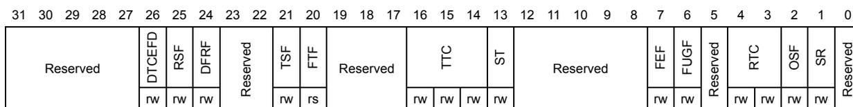
| 31 | 30 | 29 | 28 | 27 | 26 | 25 | 24 | 23 | 22 | 21 | 20 | 19 | 18 | 17 | 16 | 15 | 14 | 13 | 12 | 11 | 10 | 9 | 8 | 7 | 6 | 5 | 4 | 3 | 2 | 1 | 0 | |
| Reserved | DTCEFD | RSF | DFRF | Reserved | TSF | FTF | Reserved | TTC | ST | Reserved | FEF | FUGF | Reserved | RTC | OSF | SR | Reserved | |||||||||||||||
| rw | rw | rw | rw | rs | rw | rw | rw | rw | rw | rw | rw | rw | rw | rw | ||||||||||||||||||
Bits 31:27 Reserved, must be kept at reset value.
Bit 26 DTCEFD : Dropping of TCP/IP checksum error frames disable
When this bit is set, the core does not drop frames that only have errors detected by the receive checksum offload engine. Such frames do not have any errors (including FCS error) in the Ethernet frame received by the MAC but have errors in the encapsulated payload only. When this bit is cleared, all error frames are dropped if the FEF bit is reset.
Bit 25 RSF : Receive store and forward
When this bit is set, a frame is read from the Rx FIFO after the complete frame has been written to it, ignoring RTC bits. When this bit is cleared, the Rx FIFO operates in Cut-through mode, subject to the threshold specified by the RTC bits.
Bit 24 DFRF : Disable flushing of received frames
When this bit is set, the RxDMA does not flush any frames due to the unavailability of receive descriptors/buffers as it does normally when this bit is cleared (see Receive process suspended ).
Bits 23:22 Reserved, must be kept at reset value.
Bit 21 TSF : Transmit store and forward
When this bit is set, transmission starts when a full frame resides in the Transmit FIFO. When this bit is set, the TTC values specified by the ETH_DMAOMR register bits [16:14] are ignored.
When this bit is cleared, the TTC values specified by the ETH_DMAOMR register bits [16:14] are taken into account.
This bit should be changed only when transmission is stopped.
Bit 20 FTF : Flush transmit FIFO
When this bit is set, the transmit FIFO controller logic is reset to its default values and thus all data in the Tx FIFO are lost/flushed. This bit is cleared internally when the flushing operation is complete. The Operation mode register should not be written to until this bit is cleared.
Bits 19:17 Reserved, must be kept at reset value.
Bits 16:14 TTC : Transmit threshold controlThese three bits control the threshold level of the Transmit FIFO. Transmission starts when the frame size within the Transmit FIFO is larger than the threshold. In addition, full frames with a length less than the threshold are also transmitted. These bits are used only when the TSF bit (Bit 21) is cleared.
000: 64
001: 128
010: 192
011: 256
100: 40
101: 32
110: 24
111: 16
Bit 13 ST : Start/stop transmissionWhen this bit is set, transmission is placed in the Running state, and the DMA checks the transmit list at the current position for a frame to be transmitted. Descriptor acquisition is attempted either from the current position in the list, which is the transmit list base address set by the ETH_DMATDLAR register, or from the position retained when transmission was stopped previously. If the current descriptor is not owned by the DMA, transmission enters the Suspended state and the transmit buffer unavailable bit (ETH_DMASR [2]) is set. The Start Transmission command is effective only when transmission is stopped. If the command is issued before setting the DMA ETH_DMATDLAR register, the DMA behavior is unpredictable.
When this bit is cleared, the transmission process is placed in the Stopped state after completing the transmission of the current frame. The next descriptor position in the transmit list is saved, and becomes the current position when transmission is restarted. The Stop Transmission command is effective only when the transmission of the current frame is complete or when the transmission is in the Suspended state.
Bits 12:8 Reserved, must be kept at reset value.
Bit 7 FEF : Forward error framesWhen this bit is set, all frames except runt error frames are forwarded to the DMA.
When this bit is cleared, the Rx FIFO drops frames with error status (CRC error, collision error, giant frame, watchdog timeout, overflow). However, if the frame's start byte (write) pointer is already transferred to the read controller side (in Threshold mode), then the frames are not dropped. The Rx FIFO drops the error frames if that frame's start byte is not transferred (output) on the ARI bus.
Bit 6 FUGF : Forward undersized good framesWhen this bit is set, the Rx FIFO forwards undersized frames (frames with no error and length less than 64 bytes) including pad-bytes and CRC).
When this bit is cleared, the Rx FIFO drops all frames of less than 64 bytes, unless such a frame has already been transferred due to lower value of receive threshold (e.g., RTC = 01).
Bit 5 Reserved, must be kept at reset value.
Bits 4:3 RTC: Receive threshold controlThese two bits control the threshold level of the Receive FIFO. Transfer (request) to DMA starts when the frame size within the Receive FIFO is larger than the threshold. In addition, full frames with a length less than the threshold are transferred automatically.
Note: Note that value of 11 is not applicable if the configured Receive FIFO size is 128 bytes.
Note: These bits are valid only when the RSF bit is zero, and are ignored when the RSF bit is set to 1.
00: 64
01: 32
10: 96
11: 128
Bit 2 OSF: Operate on second frameWhen this bit is set, this bit instructs the DMA to process a second frame of Transmit data even before status for first frame is obtained.
Bit 1 SR: Start/stop receiveWhen this bit is set, the receive process is placed in the Running state. The DMA attempts to acquire the descriptor from the receive list and processes incoming frames. Descriptor acquisition is attempted from the current position in the list, which is the address set by the DMA ETH_DMARDLAR register or the position retained when the receive process was previously stopped. If no descriptor is owned by the DMA, reception is suspended and the receive buffer unavailable bit (ETH_DMASR [7]) is set. The Start Receive command is effective only when reception has stopped. If the command was issued before setting the DMA ETH_DMARDLAR register, the DMA behavior is unpredictable.
When this bit is cleared, RxDMA operation is stopped after the transfer of the current frame. The next descriptor position in the receive list is saved and becomes the current position when the receive process is restarted. The Stop Receive command is effective only when the Receive process is in either the Running (waiting for receive packet) or the Suspended state.
Bit 0 Reserved, must be kept at reset value. Ethernet DMA interrupt enable register (ETH_DMAIER)Address offset: 0x101C
Reset value: 0x0000 0000
The Interrupt enable register enables the interrupts reported by ETH_DMASR. Setting a bit to 1 enables a corresponding interrupt. After a hardware or software reset, all interrupts are disabled.
| 31 | 30 | 29 | 28 | 27 | 26 | 25 | 24 | 23 | 22 | 21 | 20 | 19 | 18 | 17 | 16 | 15 | 14 | 13 | 12 | 11 | 10 | 9 | 8 | 7 | 6 | 5 | 4 | 3 | 2 | 1 | 0 |
|---|---|---|---|---|---|---|---|---|---|---|---|---|---|---|---|---|---|---|---|---|---|---|---|---|---|---|---|---|---|---|---|
| Reserved | NISE | AISE | ERIE | FBEIE | Reserved | ETIE | RWTIE | RPSIE | RBUIE | RIE | TUIE | ROIE | TJTIE | TBUIE | TPSIE | TIE | |||||||||||||||
| rw | rw | rw | rw | rw | rw | rw | rw | rw | rw | rw | rw | rw | rw | rw | |||||||||||||||||
Bits 31:17 Reserved, must be kept at reset value.
Bit 16 NISE : Normal interrupt summary enable
When this bit is set, a normal interrupt is enabled. When this bit is cleared, a normal interrupt is disabled. This bit enables the following bits:
- – ETH_DMASR [0]: Transmit Interrupt
- – ETH_DMASR [2]: Transmit buffer unavailable
- – ETH_DMASR [6]: Receive interrupt
- – ETH_DMASR [14]: Early receive interrupt
Bit 15 AISE : Abnormal interrupt summary enable
When this bit is set, an abnormal interrupt is enabled. When this bit is cleared, an abnormal interrupt is disabled. This bit enables the following bits:
- – ETH_DMASR [1]: Transmit process stopped
- – ETH_DMASR [3]: Transmit jabber timeout
- – ETH_DMASR [4]: Receive overflow
- – ETH_DMASR [5]: Transmit underflow
- – ETH_DMASR [7]: Receive buffer unavailable
- – ETH_DMASR [8]: Receive process stopped
- – ETH_DMASR [9]: Receive watchdog timeout
- – ETH_DMASR [10]: Early transmit interrupt
- – ETH_DMASR [13]: Fatal bus error
Bit 14 ERIE : Early receive interrupt enable
When this bit is set with the normal interrupt summary enable bit (ETH_DMAIER register[16]), the early receive interrupt is enabled.
When this bit is cleared, the early receive interrupt is disabled.
Bit 13 FBEIE : Fatal bus error interrupt enable
When this bit is set with the abnormal interrupt summary enable bit (ETH_DMAIER register[15]), the fatal bus error interrupt is enabled.
When this bit is cleared, the fatal bus error enable interrupt is disabled.
Bits 12:11 Reserved, must be kept at reset value.
Bit 10 ETIE : Early transmit interrupt enable
When this bit is set with the abnormal interrupt summary enable bit (ETH_DMAIER register [15]), the early transmit interrupt is enabled.
When this bit is cleared, the early transmit interrupt is disabled.
Bit 9 RTWIE : receive watchdog timeout interrupt enable
When this bit is set with the abnormal interrupt summary enable bit (ETH_DMAIER register[15]), the receive watchdog timeout interrupt is enabled.
When this bit is cleared, the receive watchdog timeout interrupt is disabled.
Bit 8 RPSIE : Receive process stopped interrupt enable
When this bit is set with the abnormal interrupt summary enable bit (ETH_DMAIER register[15]), the receive stopped interrupt is enabled. When this bit is cleared, the receive stopped interrupt is disabled.
Bit 7 RBUIE : Receive buffer unavailable interrupt enable
When this bit is set with the abnormal interrupt summary enable bit (ETH_DMAIER register[15]), the receive buffer unavailable interrupt is enabled.
When this bit is cleared, the receive buffer unavailable interrupt is disabled.
Bit 6 RIE : Receive interrupt enable
When this bit is set with the normal interrupt summary enable bit (ETH_DMAIER register[16]), the receive interrupt is enabled.
When this bit is cleared, the receive interrupt is disabled.
Bit 5 TUIE : Underflow interrupt enable
When this bit is set with the abnormal interrupt summary enable bit (ETH_DMAIER register[15]), the transmit underflow interrupt is enabled.
When this bit is cleared, the underflow interrupt is disabled.
Bit 4 ROIE : Overflow interrupt enable
When this bit is set with the abnormal interrupt summary enable bit (ETH_DMAIER register[15]), the receive overflow interrupt is enabled.
When this bit is cleared, the overflow interrupt is disabled.
Bit 3 TJTIE : Transmit jabber timeout interrupt enable
When this bit is set with the abnormal interrupt summary enable bit (ETH_DMAIER register[15]), the transmit jabber timeout interrupt is enabled.
When this bit is cleared, the transmit jabber timeout interrupt is disabled.
Bit 2 TBUIE : Transmit buffer unavailable interrupt enable
When this bit is set with the normal interrupt summary enable bit (ETH_DMAIER register[16]), the transmit buffer unavailable interrupt is enabled.
When this bit is cleared, the transmit buffer unavailable interrupt is disabled.
Bit 1 TPSIE : Transmit process stopped interrupt enable
When this bit is set with the abnormal interrupt summary enable bit (ETH_DMAIER register[15]), the transmission stopped interrupt is enabled.
When this bit is cleared, the transmission stopped interrupt is disabled.
Bit 0 TIE : Transmit interrupt enable
When this bit is set with the normal interrupt summary enable bit (ETH_DMAIER register[16]), the transmit interrupt is enabled.
When this bit is cleared, the transmit interrupt is disabled.
The Ethernet interrupt is generated only when the TSTS or PMTS bits of the DMA Status register is asserted with their corresponding interrupt are unmasked, or when the NIS/AIS Status bit is asserted and the corresponding Interrupt Enable bits (NISE/AISE) are enabled.
Ethernet DMA missed frame and buffer overflow counter register (ETH_DMAMFBOCR)
Address offset: 0x1020
Reset value: 0x0000 0000
The DMA maintains two counters to track the number of missed frames during reception. This register reports the current value of the counter. The counter is used for diagnostic purposes. Bits [15:0] indicate missed frames due to the STM32F107xx buffer being unavailable (no receive descriptor was available). Bits [27:17] indicate missed frames due to Rx FIFO overflow conditions and runt frames (good frames of less than 64 bytes).
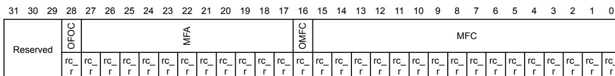
| 31 | 30 | 29 | 28 | 27 | 26 | 25 | 24 | 23 | 22 | 21 | 20 | 19 | 18 | 17 | 16 | 15 | 14 | 13 | 12 | 11 | 10 | 9 | 8 | 7 | 6 | 5 | 4 | 3 | 2 | 1 | 0 |
| Reserved | OFOC | MFA | OMFC | MFC | |||||||||||||||||||||||||||
| rc_r | rc_r | rc_r | rc_r | rc_r | rc_r | rc_r | rc_r | rc_r | rc_r | rc_r | rc_r | rc_r | rc_r | rc_r | rc_r | rc_r | rc_r | rc_r | rc_r | rc_r | rc_r | rc_r | rc_r | rc_r | rc_r | rc_r | rc_r | ||||
Bits 31:29 Reserved, must be kept at reset value.
Bit 28 OFOC : Overflow bit for FIFO overflow counter
Bits 27:17 MFA : Missed frames by the application
Indicates the number of frames missed by the application
Bit 16 OMFC : Overflow bit for missed frame counter
Bits 15:0 MFC : Missed frames by the controller
Indicates the number of frames missed by the Controller due to the host receive buffer being unavailable. This counter is incremented each time the DMA discards an incoming frame.
Ethernet DMA current host transmit descriptor register (ETH_DMACHTDR)
Address offset: 0x1048
Reset value: 0x0000 0000
The Current host transmit descriptor register points to the start address of the current transmit descriptor read by the DMA.

| 31 | 30 | 29 | 28 | 27 | 26 | 25 | 24 | 23 | 22 | 21 | 20 | 19 | 18 | 17 | 16 | 15 | 14 | 13 | 12 | 11 | 10 | 9 | 8 | 7 | 6 | 5 | 4 | 3 | 2 | 1 | 0 |
| HTDAP | |||||||||||||||||||||||||||||||
| r | r | r | r | r | r | r | r | r | r | r | r | r | r | r | r | r | r | r | r | r | r | r | r | r | r | r | r | r | r | r | r |
Bits 31:0 HTDAP : Host transmit descriptor address pointer
Cleared . Pointer updated by DMA during operation.
Ethernet DMA current host receive descriptor register (ETH_DMACHRDR)
Address offset: 0x104C
Reset value: 0x0000 0000
The Current host receive descriptor register points to the start address of the current receive descriptor read by the DMA.

| 31 | 30 | 29 | 28 | 27 | 26 | 25 | 24 | 23 | 22 | 21 | 20 | 19 | 18 | 17 | 16 | 15 | 14 | 13 | 12 | 11 | 10 | 9 | 8 | 7 | 6 | 5 | 4 | 3 | 2 | 1 | 0 | |
| HRDAP | ||||||||||||||||||||||||||||||||
| r | r | r | r | r | r | r | r | r | r | r | r | r | r | r | r | r | r | r | r | r | r | r | r | r | r | r | r | r | r | r | r | r |
Bits 31:0 HRDAP : Host receive descriptor address pointer
Cleared On Reset. Pointer updated by DMA during operation.
Ethernet DMA current host transmit buffer address register
(ETH_DMACHTBAR)
Address offset: 0x1050
Reset value: 0x0000 0000
The Current host transmit buffer address register points to the current transmit buffer address being read by the DMA.

| 31 | 30 | 29 | 28 | 27 | 26 | 25 | 24 | 23 | 22 | 21 | 20 | 19 | 18 | 17 | 16 | 15 | 14 | 13 | 12 | 11 | 10 | 9 | 8 | 7 | 6 | 5 | 4 | 3 | 2 | 1 | 0 | |
| HTBAP | ||||||||||||||||||||||||||||||||
| r | r | r | r | r | r | r | r | r | r | r | r | r | r | r | r | r | r | r | r | r | r | r | r | r | r | r | r | r | r | r | r | r |
Bits 31:0 HTBAP : Host transmit buffer address pointer
Cleared On Reset. Pointer updated by DMA during operation.
Ethernet DMA current host receive buffer address register
(ETH_DMACHRBAR)
Address offset: 0x1054
Reset value: 0x0000 0000
The current host receive buffer address register points to the current receive buffer address being read by the DMA.

| 31 | 30 | 29 | 28 | 27 | 26 | 25 | 24 | 23 | 22 | 21 | 20 | 19 | 18 | 17 | 16 | 15 | 14 | 13 | 12 | 11 | 10 | 9 | 8 | 7 | 6 | 5 | 4 | 3 | 2 | 1 | 0 | |
| HRBAP | ||||||||||||||||||||||||||||||||
| r | r | r | r | r | r | r | r | r | r | r | r | r | r | r | r | r | r | r | r | r | r | r | r | r | r | r | r | r | r | r | r | r |
Bits 31:0 HRBAP : Host receive buffer address pointer
Cleared On Reset. Pointer updated by DMA during operation.
29.8.5 Ethernet register maps
Table 218 gives the ETH register map and reset values.
Table 218. Ethernet register map and reset values
| Offset | Register | 31 | 30 | 29 | 28 | 27 | 26 | 25 | 24 | 23 | 22 | 21 | 20 | 19 | 18 | 17 | 16 | 15 | 14 | 13 | 12 | 11 | 10 | 9 | 8 | 7 | 6 | 5 | 4 | 3 | 2 | 1 | 0 | ||
|---|---|---|---|---|---|---|---|---|---|---|---|---|---|---|---|---|---|---|---|---|---|---|---|---|---|---|---|---|---|---|---|---|---|---|---|
| 0x00 | ETH_MACCCR | Reserved | WD | JD | Reserved | IFG | CSD | Reserved | FES | ROD | LM | DM | IPCO | RD | Reserved | APCS | Reserved | BL | DC | TE | RE | Reserved | |||||||||||||
| Reset value | 0 | 0 | 0 | 0 | 0 | 0 | 0 | 0 | 0 | 0 | 0 | 0 | 0 | 0 | 0 | 0 | 0 | 0 | 0 | 0 | |||||||||||||||
| 0x04 | ETH_MACFFR | RA | Reserved | HPF | SAF | Reserved | PCF | BFD | Reserved | PAM | DAIF | HM | HU | PM | |||||||||||||||||||||
| Reset value | 0 | 0 | 0 | 0 | 0 | 0 | 0 | 0 | 0 | 0 | 0 | 0 | 0 | ||||||||||||||||||||||
| 0x08 | ETH_MACHTHR | HTH[31:0] | |||||||||||||||||||||||||||||||||
| Reset value | 0 | 0 | 0 | 0 | 0 | 0 | 0 | 0 | 0 | 0 | 0 | 0 | 0 | 0 | 0 | 0 | 0 | 0 | 0 | 0 | 0 | 0 | 0 | 0 | 0 | 0 | 0 | 0 | 0 | 0 | 0 | 0 | |||
| 0x0C | ETH_MACHTLR | HTL[31:0] | |||||||||||||||||||||||||||||||||
| Reset value | 0 | 0 | 0 | 0 | 0 | 0 | 0 | 0 | 0 | 0 | 0 | 0 | 0 | 0 | 0 | 0 | 0 | 0 | 0 | 0 | 0 | 0 | 0 | 0 | 0 | 0 | 0 | 0 | 0 | 0 | 0 | 0 | |||
| 0x10 | ETH_MACMIAR | Reserved | PA | MR | Reserved | CR | MWB | MB | |||||||||||||||||||||||||||
| Reset value | 0 | 0 | 0 | 0 | 0 | 0 | 0 | 0 | 0 | 0 | 0 | 0 | 0 | 0 | 0 | ||||||||||||||||||||
| 0x14 | ETH_MACMIIDR | Reserved | MD | ||||||||||||||||||||||||||||||||
| Reset value | 0 | 0 | 0 | 0 | 0 | 0 | 0 | 0 | 0 | 0 | 0 | 0 | 0 | 0 | 0 | 0 | |||||||||||||||||||
| 0x18 | ETH_MACFCR | PT | Reserved | ZQPD | Reserved | PLT | UPFD | RFCE | TFCE | FCB/BPA | |||||||||||||||||||||||||
| Reset value | 0 | 0 | 0 | 0 | 0 | 0 | 0 | 0 | 0 | 0 | 0 | 0 | 0 | 0 | 0 | 0 | 0 | 0 | 0 | 0 | 0 | 0 | 0 | ||||||||||||
| 0x1C | ETH_MACVLANTR | Reserved | VLANTC | VLANTI | |||||||||||||||||||||||||||||||
| Reset value | 0 | 0 | 0 | 0 | 0 | 0 | 0 | 0 | 0 | 0 | 0 | 0 | 0 | 0 | 0 | 0 | 0 | ||||||||||||||||||
| 0x28 | ETH_MACRWUFFR | Frame filter reg0\Frame filter reg1\Frame filter reg2\Frame filter reg3\Frame filter reg4\...\Frame filter reg7 | |||||||||||||||||||||||||||||||||
| Reset value | 0 | ||||||||||||||||||||||||||||||||||
| 0x2C | ETH_MACPMTCSR | WFFRPR | Reserved | GU | Reserved | WFR | MPR | Reserved | WFE | MPE | PD | ||||||||||||||||||||||||
| Reset value | 0 | 0 | 0 | 0 | 0 | 0 | 0 | ||||||||||||||||||||||||||||
| 0x38 | ETH_MACSR | Not applicable | TSTS | Reserved | MMCTS | MMCRS | MMCS | PMTS | Reserved | ||||||||||||||||||||||||||
| Reset value | 0 | 0 | 0 | 0 | 0 | ||||||||||||||||||||||||||||||
| 0x3C | ETH_MACIMR | Not applicable | TSTIM | Reserved | PMTIM | Reserved | |||||||||||||||||||||||||||||
| Reset value | 0 | 0 | |||||||||||||||||||||||||||||||||
| 0x40 | ETH_MACA0HR | MO | Reserved | MACA0H | |||||||||||||||||||||||||||||||
| Reset value | 1 | 0 | 0 | 0 | 0 | 0 | 0 | 0 | 0 | 0 | 0 | 0 | 0 | 0 | 0 | 0 | 1 | 1 | 1 | 1 | 1 | 1 | 1 | 1 | 1 | 1 | 1 | 1 | 1 | 1 | 1 | 1 | |||
| 0x44 | ETH_MACA0LR | MACA0L | |||||||||||||||||||||||||||||||||
| Reset value | 1 | 1 | 1 | 1 | 1 | 1 | 1 | 1 | 1 | 1 | 1 | 1 | 1 | 1 | 1 | 1 | 1 | 1 | 1 | 1 | 1 | 1 | 1 | 1 | 1 | 1 | 1 | 1 | 1 | 1 | 1 | 1 | |||
| 0x48 | ETH_MACA1HR | AE | SA | MBC[6:0] | Reserved | MACA1H | |||||||||||||||||||||||||||||
| Reset value | 0 | 0 | 0 | 0 | 0 | 0 | 0 | 0 | 0 | 1 | 1 | 1 | 1 | 1 | 1 | 1 | 1 | 1 | 1 | 1 | 1 | 1 | 1 | 1 | 1 | ||||||||||
| 0x4C | ETH_MACA1LR | MACA1L | |||||||||||||||||||||||||||||||||
| Reset value | 1 | 1 | 1 | 1 | 1 | 1 | 1 | 1 | 1 | 1 | 1 | 1 | 1 | 1 | 1 | 1 | 1 | 1 | 1 | 1 | 1 | 1 | 1 | 1 | 1 | 1 | 1 | 1 | 1 | 1 | 1 | 1 | |||
| 0x50 | ETH_MACA2HR | AE | SA | MBC | Reserved | MACA2H | |||||||||||||||||||||||||||||
| Reset value | 0 | 0 | 0 | 0 | 0 | 0 | 0 | 0 | 0 | 1 | 1 | 1 | 1 | 1 | 1 | 1 | 1 | 1 | 1 | 1 | 1 | 1 | 1 | 1 | 1 | ||||||||||
| Offset | Register | 31 | 30 | 29 | 28 | 27 | 26 | 25 | 24 | 23 | 22 | 21 | 20 | 19 | 18 | 17 | 16 | 15 | 14 | 13 | 12 | 11 | 10 | 9 | 8 | 7 | 6 | 5 | 4 | 3 | 2 | 1 | 0 | |
|---|---|---|---|---|---|---|---|---|---|---|---|---|---|---|---|---|---|---|---|---|---|---|---|---|---|---|---|---|---|---|---|---|---|---|
| 0x54 | ETH_MACA2LR | MACA2L | ||||||||||||||||||||||||||||||||
| Reset value | 1 | 1 | 1 | 1 | 1 | 1 | 1 | 1 | 1 | 1 | 1 | 1 | 1 | 1 | 1 | 1 | 1 | 1 | 1 | 1 | 1 | 1 | 1 | 1 | 1 | 1 | 1 | 1 | 1 | 1 | 1 | 1 | ||
| 0x58 | ETH_MACA3HR | AE | SA | MBC | Reserved | MACA3H | ||||||||||||||||||||||||||||
| Reset value | 0 | 0 | 0 | 0 | 0 | 0 | 0 | 0 | 1 | 1 | 1 | 1 | 1 | 1 | 1 | 1 | 1 | 1 | 1 | 1 | 1 | 1 | 1 | 1 | ||||||||||
| 0x5C | ETH_MACA3LR | MACA3L | ||||||||||||||||||||||||||||||||
| Reset value | 1 | 1 | 1 | 1 | 1 | 1 | 1 | 1 | 1 | 1 | 1 | 1 | 1 | 1 | 1 | 1 | 1 | 1 | 1 | 1 | 1 | 1 | 1 | 1 | 1 | 1 | 1 | 1 | 1 | 1 | 1 | 1 | ||
| 0x100 | ETH_MMCCR | Reserved | MCF | ROR | CSR | CR | ||||||||||||||||||||||||||||
| Reset value | 0 | 0 | 0 | 0 | ||||||||||||||||||||||||||||||
| 0x104 | ETH_MMCRIR | Reserved | RGUFS | Reserved | RFAES | RFCES | Reserved | |||||||||||||||||||||||||||
| Reset value | 0 | 0 | 0 | |||||||||||||||||||||||||||||||
| 0x108 | ETH_MMCTIR | Reserved | TGFS | Reserved | TGFMSCS | TGFSCS | Reserved | |||||||||||||||||||||||||||
| Reset value | 0 | 0 | 0 | |||||||||||||||||||||||||||||||
| 0x10C | ETH_MMCRIMR | Reserved | RGUFM | Reserved | RFAEM | RFCEM | Reserved | |||||||||||||||||||||||||||
| Reset value | 0 | 0 | 0 | |||||||||||||||||||||||||||||||
| 0x110 | ETH_MMCTIMR | Reserved | TGFM | Reserved | TGFMSCM | TGFSCM | Reserved | |||||||||||||||||||||||||||
| Reset value | 0 | 0 | 0 | |||||||||||||||||||||||||||||||
| 0x14C | ETH_MMCTGFS CCR | TGFSCC | ||||||||||||||||||||||||||||||||
| Reset value | 0 | 0 | 0 | 0 | 0 | 0 | 0 | 0 | 0 | 0 | 0 | 0 | 0 | 0 | 0 | 0 | 0 | 0 | 0 | 0 | 0 | 0 | 0 | 0 | 0 | 0 | 0 | 0 | 0 | 0 | 0 | 0 | ||
| 0x150 | ETH_MMCTGF MSCR | TGFMSCC | ||||||||||||||||||||||||||||||||
| Reset value | 0 | 0 | 0 | 0 | 0 | 0 | 0 | 0 | 0 | 0 | 0 | 0 | 0 | 0 | 0 | 0 | 0 | 0 | 0 | 0 | 0 | 0 | 0 | 0 | 0 | 0 | 0 | 0 | 0 | 0 | 0 | 0 | ||
| 0x168 | ETH_MMCTGF CR | TGFC | ||||||||||||||||||||||||||||||||
| Reset value | 0 | 0 | 0 | 0 | 0 | 0 | 0 | 0 | 0 | 0 | 0 | 0 | 0 | 0 | 0 | 0 | 0 | 0 | 0 | 0 | 0 | 0 | 0 | 0 | 0 | 0 | 0 | 0 | 0 | 0 | 0 | 0 | ||
| 0x194 | ETH_MMCRFC ECR | RFCEC | ||||||||||||||||||||||||||||||||
| Reset value | 0 | 0 | 0 | 0 | 0 | 0 | 0 | 0 | 0 | 0 | 0 | 0 | 0 | 0 | 0 | 0 | 0 | 0 | 0 | 0 | 0 | 0 | 0 | 0 | 0 | 0 | 0 | 0 | 0 | 0 | 0 | 0 | ||
| 0x198 | ETH_MMCRFAE CR | RFAEC | ||||||||||||||||||||||||||||||||
| Reset value | 0 | 0 | 0 | 0 | 0 | 0 | 0 | 0 | 0 | 0 | 0 | 0 | 0 | 0 | 0 | 0 | 0 | 0 | 0 | 0 | 0 | 0 | 0 | 0 | 0 | 0 | 0 | 0 | 0 | 0 | 0 | 0 | ||
| 0x1C4 | ETH_MMCRGU FCR | RGUFC | ||||||||||||||||||||||||||||||||
| Reset value | 0 | 0 | 0 | 0 | 0 | 0 | 0 | 0 | 0 | 0 | 0 | 0 | 0 | 0 | 0 | 0 | 0 | 0 | 0 | 0 | 0 | 0 | 0 | 0 | 0 | 0 | 0 | 0 | 0 | 0 | 0 | 0 | ||
| 0x700 | ETH_PTPSCR | Reserved | TTSARU | TSITE | TSSTU | TSSTI | TSFCU | TSE | ||||||||||||||||||||||||||
| Reset value | 0 | 0 | 0 | 0 | 0 | 0 | ||||||||||||||||||||||||||||
| 0x704 | ETH_PTPSSIR | Reserved | STSSI | |||||||||||||||||||||||||||||||
| Reset value | 0 | 0 | 0 | 0 | 0 | 0 | 0 | 0 | ||||||||||||||||||||||||||
Table 218. Ethernet register map and reset values (continued)
| Offset | Register | 31 | 30 | 29 | 28 | 27 | 26 | 25 | 24 | 23 | 22 | 21 | 20 | 19 | 18 | 17 | 16 | 15 | 14 | 13 | 12 | 11 | 10 | 9 | 8 | 7 | 6 | 5 | 4 | 3 | 2 | 1 | 0 | |
|---|---|---|---|---|---|---|---|---|---|---|---|---|---|---|---|---|---|---|---|---|---|---|---|---|---|---|---|---|---|---|---|---|---|---|
| 0x708 | ETH_PTPTSHR | STS[31:0] | ||||||||||||||||||||||||||||||||
| Reset value | 0 | 0 | 0 | 0 | 0 | 0 | 0 | 0 | 0 | 0 | 0 | 0 | 0 | 0 | 0 | 0 | 0 | 0 | 0 | 0 | 0 | 0 | 0 | 0 | 0 | 0 | 0 | 0 | 0 | 0 | 0 | 0 | ||
| 0x70C | ETH_PTPTSLR | STPNS | STSS | |||||||||||||||||||||||||||||||
| Reset value | 0 | 0 | 0 | 0 | 0 | 0 | 0 | 0 | 0 | 0 | 0 | 0 | 0 | 0 | 0 | 0 | 0 | 0 | 0 | 0 | 0 | 0 | 0 | 0 | 0 | 0 | 0 | 0 | 0 | 0 | 0 | 0 | ||
| 0x710 | ETH_PTPTSHUR | TSUS | ||||||||||||||||||||||||||||||||
| Reset value | 0 | 0 | 0 | 0 | 0 | 0 | 0 | 0 | 0 | 0 | 0 | 0 | 0 | 0 | 0 | 0 | 0 | 0 | 0 | 0 | 0 | 0 | 0 | 0 | 0 | 0 | 0 | 0 | 0 | 0 | 0 | 0 | ||
| 0x714 | ETH_PTPTSLUR | TSUPNS | TSUSS | |||||||||||||||||||||||||||||||
| Reset value | 0 | 0 | 0 | 0 | 0 | 0 | 0 | 0 | 0 | 0 | 0 | 0 | 0 | 0 | 0 | 0 | 0 | 0 | 0 | 0 | 0 | 0 | 0 | 0 | 0 | 0 | 0 | 0 | 0 | 0 | 0 | 0 | ||
| 0x718 | ETH_PTPTSAR | TSA | ||||||||||||||||||||||||||||||||
| Reset value | 0 | 0 | 0 | 0 | 0 | 0 | 0 | 0 | 0 | 0 | 0 | 0 | 0 | 0 | 0 | 0 | 0 | 0 | 0 | 0 | 0 | 0 | 0 | 0 | 0 | 0 | 0 | 0 | 0 | 0 | 0 | 0 | ||
| 0x71C | ETH_PTPTTHR | TTSH | ||||||||||||||||||||||||||||||||
| Reset value | 0 | 0 | 0 | 0 | 0 | 0 | 0 | 0 | 0 | 0 | 0 | 0 | 0 | 0 | 0 | 0 | 0 | 0 | 0 | 0 | 0 | 0 | 0 | 0 | 0 | 0 | 0 | 0 | 0 | 0 | 0 | 0 | ||
| 0x720 | ETH_PTPTTLR | TTSL | ||||||||||||||||||||||||||||||||
| Reset value | 0 | 0 | 0 | 0 | 0 | 0 | 0 | 0 | 0 | 0 | 0 | 0 | 0 | 0 | 0 | 0 | 0 | 0 | 0 | 0 | 0 | 0 | 0 | 0 | 0 | 0 | 0 | 0 | 0 | 0 | 0 | 0 | ||
| 0x1000 | ETH_DMABMR | Reserved | AAB | FPM | USP | RDP | FB | PM | PBL | EDFE | DSL | DA | SR | |||||||||||||||||||||
| Reset value | 0 | 0 | 0 | 0 | 0 | 0 | 0 | 0 | 1 | 0 | 0 | 0 | 0 | 0 | 0 | 0 | 0 | 1 | 0 | 0 | 0 | 0 | 0 | 0 | 1 | |||||||||
| 0x1004 | ETH_DMATPDR | TPD | ||||||||||||||||||||||||||||||||
| Reset value | 0 | 0 | 0 | 0 | 0 | 0 | 0 | 0 | 0 | 0 | 0 | 0 | 0 | 0 | 0 | 0 | 0 | 0 | 0 | 0 | 0 | 0 | 0 | 0 | 0 | 0 | 0 | 0 | 0 | 0 | 0 | 0 | ||
| 0x1008 | ETH_DMARPDR | RPD | ||||||||||||||||||||||||||||||||
| Reset value | 0 | 0 | 0 | 0 | 0 | 0 | 0 | 0 | 0 | 0 | 0 | 0 | 0 | 0 | 0 | 0 | 0 | 0 | 0 | 0 | 0 | 0 | 0 | 0 | 0 | 0 | 0 | 0 | 0 | 0 | 0 | 0 | ||
| 0x100C | ETH_DMARDLAR | SRL | ||||||||||||||||||||||||||||||||
| Reset value | 0 | 0 | 0 | 0 | 0 | 0 | 0 | 0 | 0 | 0 | 0 | 0 | 0 | 0 | 0 | 0 | 0 | 0 | 0 | 0 | 0 | 0 | 0 | 0 | 0 | 0 | 0 | 0 | 0 | 0 | 0 | 0 | ||
| 0x1010 | ETH_DMATDLAR | STL | ||||||||||||||||||||||||||||||||
| Reset value | 0 | 0 | 0 | 0 | 0 | 0 | 0 | 0 | 0 | 0 | 0 | 0 | 0 | 0 | 0 | 0 | 0 | 0 | 0 | 0 | 0 | 0 | 0 | 0 | 0 | 0 | 0 | 0 | 0 | 0 | 0 | 0 | ||
| 0x1014 | ETH_DMASR | Reserved | TSTS | PMTS | MMCS | Reserved | EBS | TPS | RPS | NIS | AIS | ERS | FBES | Reserved | ETS | RWTS | RPSS | RBUS | RS | TUS | ROS | TJTS | TBUS | TPSS | TS | |||||||||
| Reset value | 0 | 0 | 0 | 0 | 0 | 0 | 0 | 0 | 0 | 0 | 0 | 0 | 0 | 0 | 0 | 0 | 0 | 0 | 0 | 0 | 0 | 0 | 0 | 0 | 0 | 0 | 0 | |||||||
| 0x1018 | ETH_DMAOMR | Reserved | DTCEFD | RSF | DFRF | Reserved | TSF | FTF | Reserved | TTC | ST | Reserved | FEF | FUGF | Reserved | RTC | OSF | SR | Reserved | |||||||||||||||
| Reset value | 0 | 0 | 0 | 0 | 0 | 0 | 0 | 0 | 0 | 0 | 0 | 0 | 0 | 0 | 0 | 0 | ||||||||||||||||||
| 0x101C | ETH_DMAIER | Reserved | NISE | AISE | ERIE | FBEIE | Reserved | ETIE | RWTIE | RPSIE | RBUIE | RIE | TUIE | ROIE | TJTIE | TBUIE | TPSIE | TIE | ||||||||||||||||
| Reset value | 0 | 0 | 0 | 0 | 0 | 0 | 0 | 0 | 0 | 0 | 0 | 0 | 0 | 0 | 0 | |||||||||||||||||||
| 0x1020 | ETH_DMAMFBOCR | Reserved | OFOC | MFA | OMFC | MFC | ||||||||||||||||||||||||||||
| Reset value | 0 | 0 | 0 | 0 | 0 | 0 | 0 | 0 | 0 | 0 | 0 | 0 | 0 | 0 | 0 | 0 | 0 | 0 | 0 | 0 | 0 | 0 | 0 | 0 | 0 | 0 | 0 | 0 | 0 | 0 | ||||
| 0x1048 | ETH_DMACHTD R | HTDAP | ||||||||||||||||||||||||||||||||
| Reset value | 0 | 0 | 0 | 0 | 0 | 0 | 0 | 0 | 0 | 0 | 0 | 0 | 0 | 0 | 0 | 0 | 0 | 0 | 0 | 0 | 0 | 0 | 0 | 0 | 0 | 0 | 0 | 0 | 0 | 0 | 0 | 0 | ||
Table 218. Ethernet register map and reset values (continued)
| Offset | Register | 31 | 30 | 29 | 28 | 27 | 26 | 25 | 24 | 23 | 22 | 21 | 20 | 19 | 18 | 17 | 16 | 15 | 14 | 13 | 12 | 11 | 10 | 9 | 8 | 7 | 6 | 5 | 4 | 3 | 2 | 1 | 0 |
|---|---|---|---|---|---|---|---|---|---|---|---|---|---|---|---|---|---|---|---|---|---|---|---|---|---|---|---|---|---|---|---|---|---|
| 0x104C | ETH_DMACHR DR | HRDAP | |||||||||||||||||||||||||||||||
| Reset value | 0 | 0 | 0 | 0 | 0 | 0 | 0 | 0 | 0 | 0 | 0 | 0 | 0 | 0 | 0 | 0 | 0 | 0 | 0 | 0 | 0 | 0 | 0 | 0 | 0 | 0 | 0 | 0 | 0 | 0 | 0 | 0 | |
| 0x1050 | ETH_DMACHTB AR | HTBAP | |||||||||||||||||||||||||||||||
| Reset value | 0 | 0 | 0 | 0 | 0 | 0 | 0 | 0 | 0 | 0 | 0 | 0 | 0 | 0 | 0 | 0 | 0 | 0 | 0 | 0 | 0 | 0 | 0 | 0 | 0 | 0 | 0 | 0 | 0 | 0 | 0 | 0 | |
| 0x1054 | ETH_DMACHRB AR | HRBAP | |||||||||||||||||||||||||||||||
| Reset value | 0 | 0 | 0 | 0 | 0 | 0 | 0 | 0 | 0 | 0 | 0 | 0 | 0 | 0 | 0 | 0 | 0 | 0 | 0 | 0 | 0 | 0 | 0 | 0 | 0 | 0 | 0 | 0 | 0 | 0 | 0 | 0 | |
Refer to Section 3.3: Memory map for the register boundary addresses.