26. Inter-integrated circuit (I2C) interface
Low-density devices are STM32F101xx, STM32F102xx and STM32F103xx microcontrollers where the Flash memory density ranges between 16 and 32 Kbytes.
Medium-density devices are STM32F101xx, STM32F102xx and STM32F103xx microcontrollers where the Flash memory density ranges between 64 and 128 Kbytes.
High-density devices are STM32F101xx and STM32F103xx microcontrollers where the Flash memory density ranges between 256 and 512 Kbytes.
XL-density devices are STM32F101xx and STM32F103xx microcontrollers where the Flash memory density ranges between 768 Kbytes and 1 Mbyte.
Connectivity line devices are STM32F105xx and STM32F107xx microcontrollers.
This section applies to the whole STM32F10xxx family, unless otherwise specified.
26.1 I 2 C introduction
I 2 C (inter-integrated circuit) bus Interface serves as an interface between the microcontroller and the serial I 2 C bus. It provides multimaster capability, and controls all I 2 C bus-specific sequencing, protocol, arbitration and timing. It supports the standard mode (Sm, up to 100 kHz) and Fm mode (Fm, up to 400 kHz).
It may be used for a variety of purposes, including CRC generation and verification, SMBus (system management bus) and PMBus (power management bus).
Depending on specific device implementation DMA capability can be available for reduced CPU overload.
26.2 I 2 C main features
- • Parallel-bus/I 2 C protocol converter
- • Multimaster capability: the same interface can act as Master or Slave
- • I
2
C Master features:
- – Clock generation
- – Start and Stop generation
- • I
2
C Slave features:
- – Programmable I 2 C Address detection
- – Dual Addressing Capability to acknowledge 2 slave addresses
- – Stop bit detection
- • Generation and detection of 7-bit/10-bit addressing and General Call
- • Supports different communication speeds:
- – Standard Speed (up to 100 kHz)
- – Fast Speed (up to 400 kHz)
- • Analog noise filter
- • Status flags:
- – Transmitter/Receiver mode flag
- – End-of-Byte transmission flag
- – I 2 C busy flag
- • Error flags:
- – Arbitration lost condition for master mode
- – Acknowledgment failure after address/ data transmission
- – Detection of misplaced start or stop condition
- – Overrun/Underrun if clock stretching is disabled
- • 2 Interrupt vectors:
- – 1 Interrupt for successful address/ data communication
- – 1 Interrupt for error condition
- • Optional clock stretching
- • 1-byte buffer with DMA capability
- • Configurable PEC (packet error checking) generation or verification:
- – PEC value can be transmitted as last byte in Tx mode
- – PEC error checking for last received byte
- • SMBus 2.0 Compatibility:
- – 25 ms clock low timeout delay
- – 10 ms master cumulative clock low extend time
- – 25 ms slave cumulative clock low extend time
- – Hardware PEC generation/verification with ACK control
- – Address Resolution Protocol (ARP) supported
- • PMBus Compatibility
Note: Some of the above features may not be available in certain products. The user should refer to the product data sheet, to identify the specific features supported by the I 2 C interface implementation.
26.3 I 2 C functional description
In addition to receiving and transmitting data, this interface converts it from serial to parallel format and vice versa. The interrupts are enabled or disabled by software. The interface is connected to the I 2 C bus by a data pin (SDA) and by a clock pin (SCL). It can be connected with a standard (up to 100 kHz) or fast (up to 400 kHz) I 2 C bus.
26.3.1 Mode selection
The interface can operate in one of the four following modes:
- • Slave transmitter
- • Slave receiver
- • Master transmitter
- • Master receiver
By default, it operates in slave mode. The interface automatically switches from slave to master, after it generates a START condition and from master to slave, if an arbitration loss or a Stop generation occurs, allowing multimaster capability.
Communication flow
In Master mode, the I 2 C interface initiates a data transfer and generates the clock signal. A serial data transfer always begins with a start condition and ends with a stop condition. Both start and stop conditions are generated in master mode by software.
In Slave mode, the interface is capable of recognizing its own addresses (7 or 10-bit), and the General Call address. The General Call address detection may be enabled or disabled by software.
Data and addresses are transferred as 8-bit bytes, MSB first. The first byte(s) following the start condition contain the address (one in 7-bit mode, two in 10-bit mode). The address is always transmitted in Master mode.
A 9th clock pulse follows the 8 clock cycles of a byte transfer, during which the receiver must send an acknowledge bit to the transmitter. Refer to Figure 269 .
Figure 269. I 2 C bus protocol
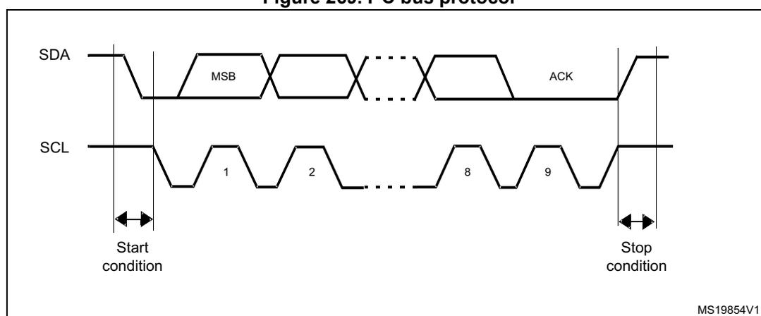
The diagram illustrates the I 2 C bus protocol timing. The top line represents the SDA (Serial Data) signal, and the bottom line represents the SCL (Serial Clock) signal. The SCL signal is a periodic clock with pulses labeled 1, 2, ..., 8, 9. The SDA signal starts high and drops to low for the start condition, then transmits the MSB (Most Significant Bit) of a byte, followed by a dashed section indicating more bits, and then goes low for the ACK (Acknowledge) signal before returning high for the stop condition. The start condition is marked with a double-headed arrow and the label 'Start condition'. The stop condition is marked with a double-headed arrow and the label 'Stop condition'. The diagram is labeled MS19854V1 in the bottom right corner.
Acknowledge may be enabled or disabled by software. The I 2 C interface addresses (dual addressing 7-bit/ 10-bit and/or general call address) can be selected by software.
The block diagram of the I 2 C interface is shown in Figure 270 .
Figure 270. I 2 C block diagram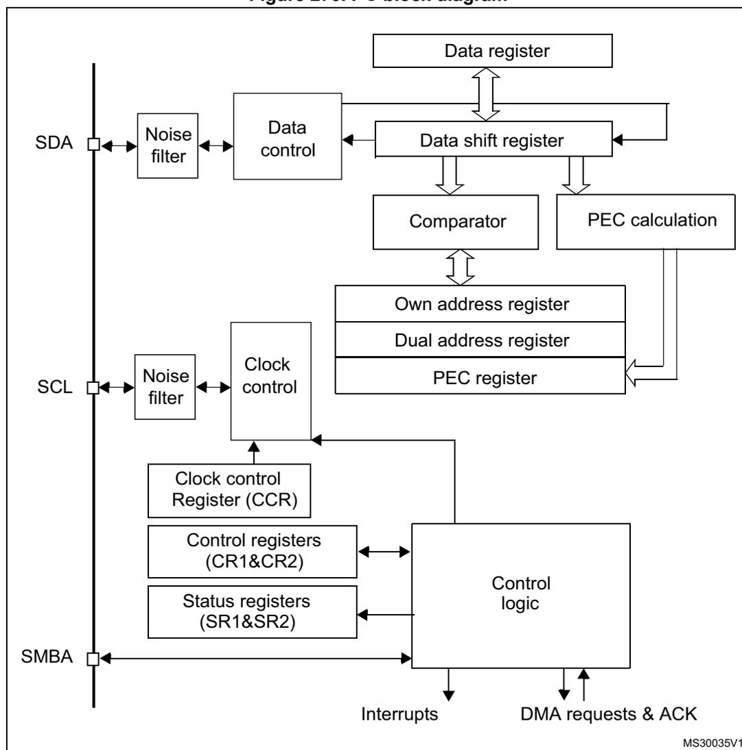
1. SMBA is an optional signal in SMBus mode. This signal is not applicable if SMBus is disabled.
26.3.2 I 2 C slave mode
By default the I 2 C interface operates in Slave mode. To switch from default Slave mode to Master mode a Start condition generation is needed.
The peripheral input clock must be programmed in the I2C_CR2 register in order to generate correct timings. The peripheral input clock frequency must be at least:
- • 2 MHz in Sm mode
- • 4 MHz in Fm mode
As soon as a start condition is detected, the address is received from the SDA line and sent to the shift register. Then it is compared with the address of the interface (OAR1) and with OAR2 (if ENDUAL=1) or the General Call address (if ENGCG = 1).
Note: In 10-bit addressing mode, the comparison includes the header sequence (11110xx0), where xx denotes the two most significant bits of the address.
Header or address not matched: the interface ignores it and waits for another Start condition.
Header matched (10-bit mode only): the interface generates an acknowledge pulse if the ACK bit is set and waits for the 8-bit slave address.
Address matched: the interface generates in sequence:
- • An acknowledge pulse if the ACK bit is set
- • The ADDR bit is set by hardware and an interrupt is generated if the ITEVFEN bit is set.
- • If ENDUAL=1, the software has to read the DUALF bit to check which slave address has been acknowledged.
In 10-bit mode, after receiving the address sequence the slave is always in Receiver mode. It will enter Transmitter mode on receiving a repeated Start condition followed by the header sequence with matching address bits and the least significant bit set (11110x1).
The TRA bit indicates whether the slave is in Receiver or Transmitter mode.
Slave transmitter
Following the address reception and after clearing ADDR, the slave sends bytes from the DR register to the SDA line via the internal shift register.
The slave stretches SCL low until ADDR is cleared and DR filled with the data to be sent (see Figure 271 Transfer sequencing EV1 EV3).
When the acknowledge pulse is received:
- • The TxE bit is set by hardware with an interrupt if the ITEVFEN and the ITBUFEN bits are set.
If TxE is set and some data were not written in the I2C_DR register before the end of the next data transmission, the BTF bit is set and the interface waits until BTF is cleared by a read to I2C_SR1 followed by a write to the I2C_DR register, stretching SCL low.
Figure 271. Transfer sequence diagram for slave transmitter
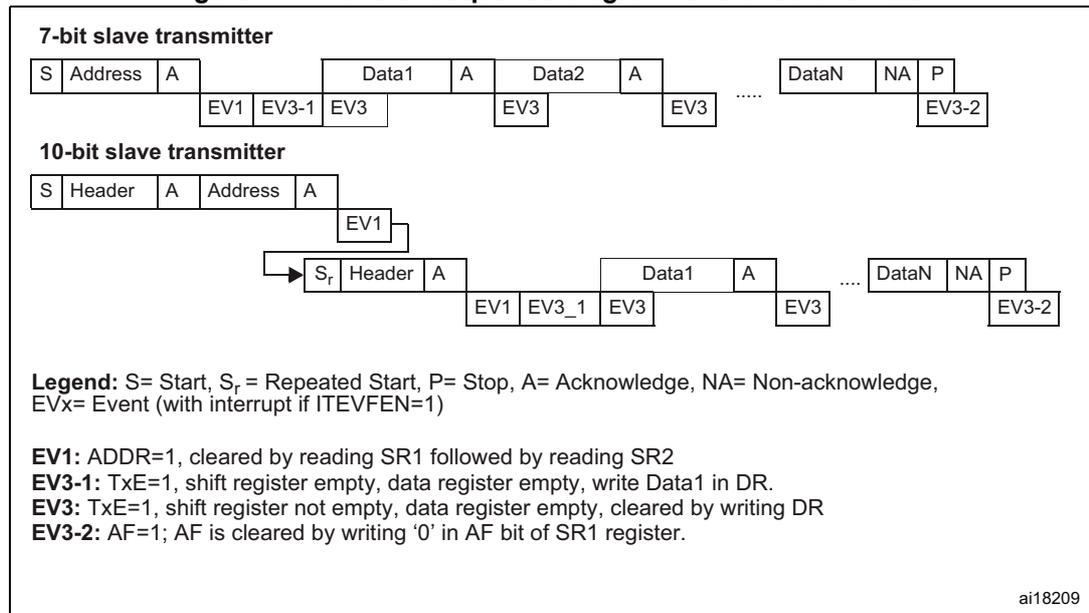
The diagram illustrates the transfer sequence for a slave transmitter in two modes:
- 7-bit slave transmitter: The sequence starts with a Start (S) condition, followed by an Address and Acknowledge (A). This is followed by a series of data blocks (Data1, Data2, ..., DataN), each consisting of data, an Acknowledge (A), and a Non-acknowledge (NA) or Stop (P) condition. Timing events are indicated below the sequence: EV1 (after Address/A), EV3-1 (after Start), EV3 (after Data1/A), EV3 (after Data2/A), EV3 (after DataN/NA), and EV3-2 (after Stop/P).
- 10-bit slave transmitter: The sequence starts with a Start (S) condition, followed by a Header and Acknowledge (A). This is followed by an Address and Acknowledge (A). A Repeated Start (Sr) condition follows, then a Header and Acknowledge (A). This is followed by a series of data blocks (Data1, ..., DataN), each consisting of data, an Acknowledge (A), and a Non-acknowledge (NA) or Stop (P) condition. Timing events are indicated below the sequence: EV1 (after Address/A), EV1 (after Sr/Header/A), EV3_1 (after Data1/A), EV3 (after DataN/NA), and EV3-2 (after Stop/P).
Legend: S= Start, Sr= Repeated Start, P= Stop, A= Acknowledge, NA= Non-acknowledge, EVx= Event (with interrupt if ITEVFEN=1)
EV1:
ADDR=1, cleared by reading SR1 followed by reading SR2
EV3-1:
TxE=1, shift register empty, data register empty, write Data1 in DR.
EV3:
TxE=1, shift register not empty, data register empty, cleared by writing DR
EV3-2:
AF=1; AF is cleared by writing '0' in AF bit of SR1 register.
ai18209
Slave receiver
Following the address reception and after clearing ADDR, the slave receives bytes from the SDA line into the DR register via the internal shift register. After each byte the interface generates in sequence:
- • An acknowledge pulse if the ACK bit is set
- • The RxNE bit is set by hardware and an interrupt is generated if the ITEVFEN and ITBUFEN bit is set.
If RxNE is set and the data in the DR register is not read before the end of the next data reception, the BTF bit is set and the interface waits until BTF is cleared by a read from I2C_SR1 followed by a read from the I2C_DR register, stretching SCL low (see Figure 272 Transfer sequencing).
Figure 272. Transfer sequence diagram for slave receiver
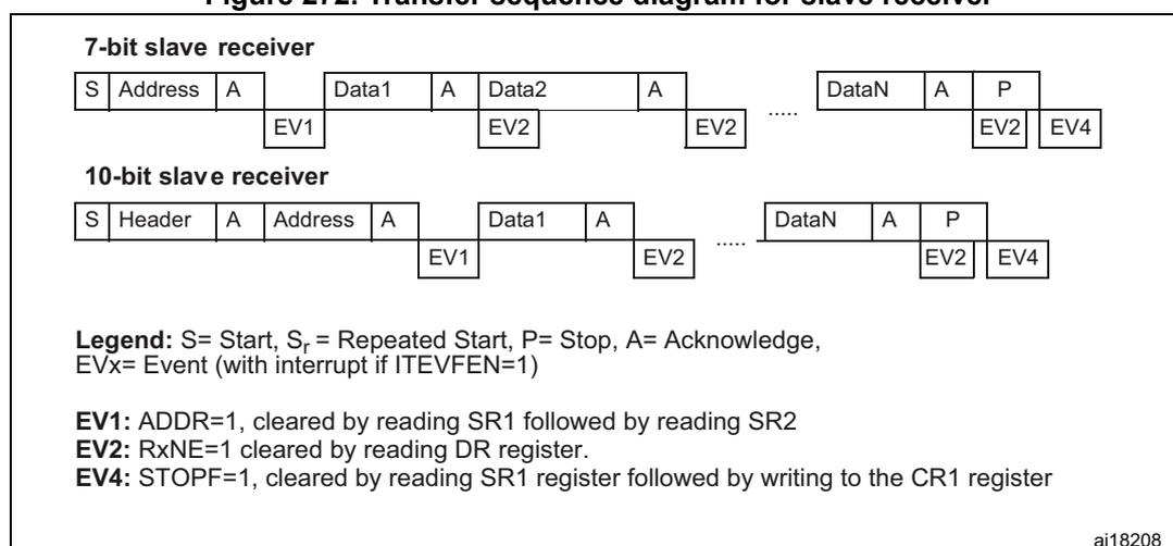
7-bit slave receiver
| S | Address | A | Data1 | A | Data2 | A | ... | DataN | A | P | ||
| EV1 | EV2 | EV2 | EV4 |
10-bit slave receiver
| S | Header | A | Address | A | Data1 | A | ... | DataN | A | P | ||
| EV1 | EV2 | EV2 | EV4 |
Legend: S= Start, Sr = Repeated Start, P= Stop, A= Acknowledge, EVx= Event (with interrupt if ITEVFEN=1)
EV1:
ADDR=1, cleared by reading SR1 followed by reading SR2
EV2:
RxNE=1 cleared by reading DR register.
EV4:
STOPF=1, cleared by reading SR1 register followed by writing to the CR1 register
ai18208
- 1. The EV1 event stretches SCL low until the end of the corresponding software sequence.
- 2. The EV2 software sequence must be completed before the end of the current byte transfer
- 3. After checking the SR1 register content, the user should perform the complete clearing sequence for each flag found set.
Thus, for ADDR and STOPF flags, the following sequence is required inside the I2C interrupt routine:READ SR1 if (ADDR == 1) {READ SR1; READ SR2} if (STOPF == 1) {READ SR1; WRITE CR1}The purpose is to make sure that both ADDR and STOPF flags are cleared if both are found set.
Closing slave communication
After the last data byte is transferred a Stop Condition is generated by the master. The interface detects this condition and sets:
- • The STOPF bit and generates an interrupt if the ITEVFEN bit is set.
The STOPF bit is cleared by a read of the SR1 register followed by a write to the CR1 register (see EV4 in Figure 272 ).
26.3.3 I 2 C master mode
In Master mode, the I 2 C interface initiates a data transfer and generates the clock signal. A serial data transfer always begins with a Start condition and ends with a Stop condition.
Master mode is selected as soon as the Start condition is generated on the bus with a START bit.
The following is the required sequence in master mode.
- • Program the peripheral input clock in I2C_CR2 register in order to generate correct timings
- • Configure the clock control registers
- • Configure the rise time register
- • Program the I2C_CR1 register to enable the peripheral
- • Set the START bit in the I2C_CR1 register to generate a Start condition
The peripheral input clock frequency must be at least:
- • 2 MHz in Sm mode
- • 4 MHz in Fm mode
SCL master clock generation
The CCR bits are used to generate the high and low level of the SCL clock, starting from the generation of the rising and falling edge (respectively). As a slave may stretch the SCL line, the peripheral checks the SCL input from the bus at the end of the time programmed in TRISE bits after rising edge generation.
- • If the SCL line is low, it means that a slave is stretching the bus, and the high level counter stops until the SCL line is detected high. This allows to guarantee the minimum HIGH period of the SCL clock parameter.
- • If the SCL line is high, the high level counter keeps on counting.
Indeed, the feedback loop from the SCL rising edge generation by the peripheral to the SCL rising edge detection by the peripheral takes time even if no slave stretches the clock. This loopback duration is linked to the SCL rising time (impacting SCL VIH input detection), plus delay due to the noise filter present on the SCL input path, plus delay due to internal SCL input synchronization with APB clock. The maximum time used by the feedback loop is programmed in the TRISE bits, so that the SCL frequency remains stable whatever the SCL rising time.
Start condition
Setting the START bit causes the interface to generate a Start condition and to switch to Master mode (MSL bit set) when the BUSY bit is cleared.
Note: In master mode, setting the START bit causes the interface to generate a ReStart condition at the end of the current byte transfer.
Once the Start condition is sent:
- • The SB bit is set by hardware and an interrupt is generated if the ITEVFEN bit is set.
Then the master waits for a read of the SR1 register followed by a write in the DR register with the Slave address (see Figure 273 and Figure 274 Transfer sequencing EV5).
Slave address transmission
Then the slave address is sent to the SDA line via the internal shift register.
- • In 10-bit addressing mode, sending the header sequence causes the following event:
- – The ADD10 bit is set by hardware and an interrupt is generated if the ITEVFEN bit is set.
Then the master waits for a read of the SR1 register followed by a write in the DR register with the second address byte (see Figure 273 and Figure 274 Transfer sequencing).
- – The ADDR bit is set by hardware and an interrupt is generated if the ITEVFEN bit is set.
Then the master waits for a read of the SR1 register followed by a read of the SR2 register (see Figure 273 and Figure 274 Transfer sequencing).
- • In 7-bit addressing mode, one address byte is sent.
As soon as the address byte is sent,
- – The ADDR bit is set by hardware and an interrupt is generated if the ITEVFEN bit is set.
Then the master waits for a read of the SR1 register followed by a read of the SR2 register (see Figure 273 and Figure 274 Transfer sequencing).
The master can decide to enter Transmitter or Receiver mode depending on the LSB of the slave address sent.
- • In 7-bit addressing mode,
- – To enter Transmitter mode, a master sends the slave address with LSB reset.
- – To enter Receiver mode, a master sends the slave address with LSB set.
- • In 10-bit addressing mode,
- – To enter Transmitter mode, a master sends the header (11110xx0) and then the slave address, (where xx denotes the two most significant bits of the address).
- – To enter Receiver mode, a master sends the header (11110xx0) and then the slave address. Then it should send a repeated Start condition followed by the header (11110xx1), (where xx denotes the two most significant bits of the address).
The TRA bit indicates whether the master is in Receiver or Transmitter mode.
Master transmitter
Following the address transmission and after clearing ADDR, the master sends bytes from the DR register to the SDA line via the internal shift register.
The master waits until the first data byte is written into I2C_DR (see Figure 273 Transfer sequencing EV8_1).
When the acknowledge pulse is received, the TxE bit is set by hardware and an interrupt is generated if the ITEVFEN and ITBUFEN bits are set.
If TxE is set and a data byte was not written in the DR register before the end of the last data transmission, BTF is set and the interface waits until BTF is cleared by a read from I2C_SR1 followed by a write to I2C_DR, stretching SCL low.
Closing the communication
After the last byte is written to the DR register, the STOP bit is set by software to generate a Stop condition (see Figure 273 Transfer sequencing EV8_2). The interface automatically goes back to slave mode (MSL bit cleared).
Note: Stop condition should be programmed during EV8_2 event, when either TxE or BTF is set.
Figure 273. Transfer sequence diagram for master transmitter
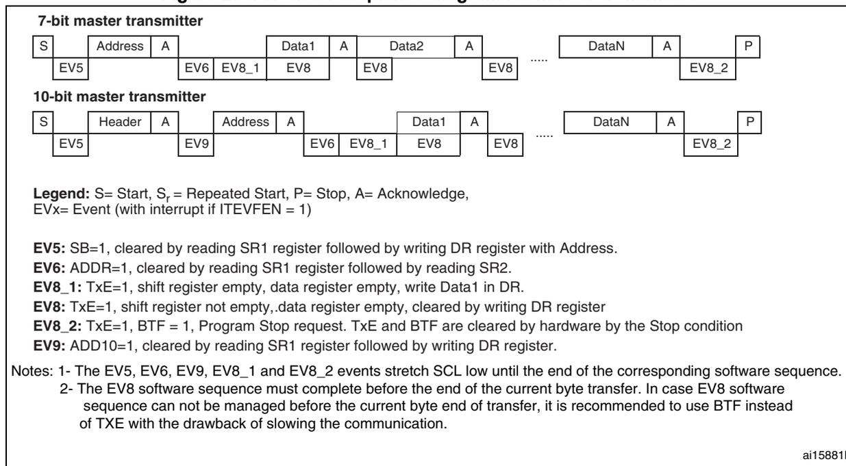
The diagram illustrates the transfer sequence for a master transmitter in two modes: 7-bit and 10-bit.
7-bit master transmitter: The sequence starts with a Start (S) condition, followed by an Address (A) and Acknowledge (A). This is followed by a series of data bytes (Data1, Data2, ..., DataN) each followed by an Acknowledge (A). The sequence ends with a Stop (P) condition. Events are indicated below the sequence: EV5 (Start), EV6 (Address), EV8_1 (Data1), EV8 (Data2), EV8 (DataN), and EV8_2 (Stop).
10-bit master transmitter: The sequence starts with a Start (S) condition, followed by a Header (A) and Acknowledge (A). This is followed by an Address (A) and Acknowledge (A). This is followed by a series of data bytes (Data1, ..., DataN) each followed by an Acknowledge (A). The sequence ends with a Stop (P) condition. Events are indicated below the sequence: EV5 (Start), EV9 (Header), EV6 (Address), EV8_1 (Data1), EV8 (DataN), and EV8_2 (Stop).
Legend: S= Start, S r = Repeated Start, P= Stop, A= Acknowledge, EVx= Event (with interrupt if ITEVFEN = 1)
EV5: SB=1, cleared by reading SR1 register followed by writing DR register with Address.
EV6: ADDR=1, cleared by reading SR1 register followed by reading SR2.
EV8_1: TxE=1, shift register empty, data register empty, write Data1 in DR.
EV8: TxE=1, shift register not empty, data register empty, cleared by writing DR register
EV8_2: TxE=1, BTF = 1, Program Stop request. TxE and BTF are cleared by hardware by the Stop condition
EV9: ADD10=1, cleared by reading SR1 register followed by writing DR register.
Notes:
- 1- The EV5, EV6, EV9, EV8_1 and EV8_2 events stretch SCL low until the end of the corresponding software sequence.
- 2- The EV8 software sequence must complete before the end of the current byte transfer. In case EV8 software sequence can not be managed before the current byte end of transfer, it is recommended to use BTF instead of TXE with the drawback of slowing the communication.
ai15881b
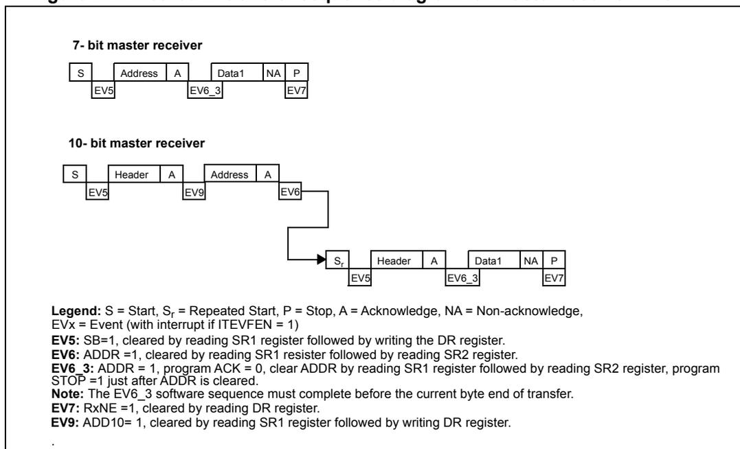
Master receiver
Following the address transmission and after clearing ADDR, the I 2 C interface enters Master Receiver mode. In this mode the interface receives bytes from the SDA line into the DR register via the internal shift register. After each byte the interface generates in sequence:
- 1. An acknowledge pulse if the ACK bit is set
- 2. The RxNE bit is set and an interrupt is generated if the ITEVFEN and ITBUFEN bits are set (see Figure 274 Transfer sequencing EV7).
If the RxNE bit is set and the data in the DR register is not read before the end of the last data reception, the BTF bit is set by hardware and the interface waits until BTF is cleared by a read in the SR1 register followed by a read in the DR register, stretching SCL low.
Closing the communication
Method 1: This method is for the case when the I2C is used with interrupts that have the highest priority in the application.
The master sends a NACK for the last byte received from the slave. After receiving this NACK, the slave releases the control of the SCL and SDA lines. Then the master can send a Stop/Restart condition.
- 1. To generate the nonacknowledge pulse after the last received data byte, the ACK bit must be cleared just after reading the second last data byte (after second last RxNE event).
- 2. To generate the Stop/Restart condition, software must set the STOP/START bit just after reading the second last data byte (after the second last RxNE event).
- 3. In case a single byte has to be received, the Acknowledge disable and the Stop condition generation are made just after EV6 (in EV6_1, just after ADDR is cleared).
After the Stop condition generation, the interface goes automatically back to slave mode (MSL bit cleared).
Figure 274. Method 1: transfer sequence diagram for master receiver
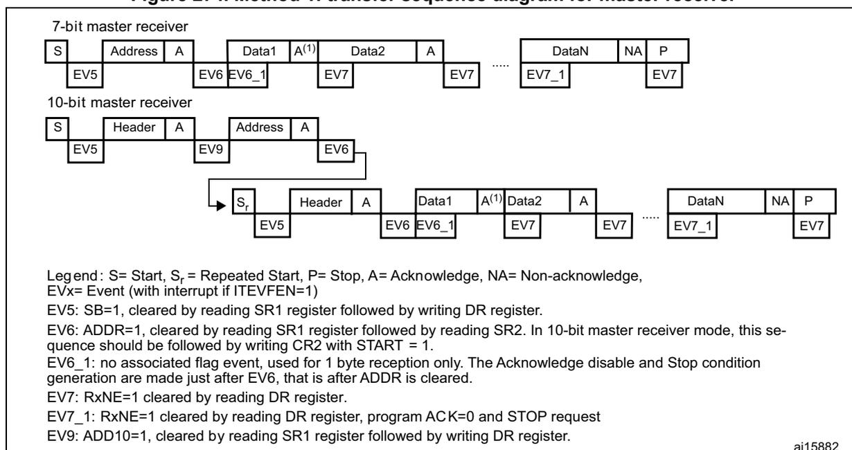
Legend: S= Start, S
r
= Repeated Start, P= Stop, A= Acknowledge, NA= Non-acknowledge,
EVx= Event (with interrupt if ITEVFEN=1)
EV5: SB=1, cleared by reading SR1 register followed by writing DR register.
EV6: ADDR=1, cleared by reading SR1 register followed by reading SR2. In 10-bit master receiver mode, this sequence should be followed by writing CR2 with START = 1.
EV6_1: no associated flag event, used for 1 byte reception only. The Acknowledge disable and Stop condition generation are made just after EV6, that is after ADDR is cleared.
EV7: RxNE=1 cleared by reading DR register.
EV7_1: RxNE=1 cleared by reading DR register, program ACK=0 and STOP request
EV9: ADD10=1, cleared by reading SR1 register followed by writing DR register.
ai15882
- 1. If a single byte is received, it is NA.
- 2. The EV5, EV6 and EV9 events stretch SCL low until the end of the corresponding software sequence.
- 3. The EV7 software sequence must complete before the end of the current byte transfer. In case EV7 software sequence can not be managed before the current byte end of transfer, it is recommended to use BTF instead of RXNE with the drawback of slowing the communication.
- 4. The EV6_1 or EV7_1 software sequence must complete before the ACK pulse of the current byte transfer.
Method 2: This method is for the case when the I2C is used with interrupts that do not have the highest priority in the application or when the I2C is used with polling.
With this method, DataN_2 is not read, so that after DataN_1, the communication is stretched (both RxNE and BTF are set). Then, clear the ACK bit before reading DataN-2 in DR to ensure it is be cleared before the DataN Acknowledge pulse. After that, just after reading DataN_2, set the STOP/ START bit and read DataN_1. After RxNE is set, read DataN. This is illustrated below:
Figure 275. Method 2: transfer sequence diagram for master receiver when N>2
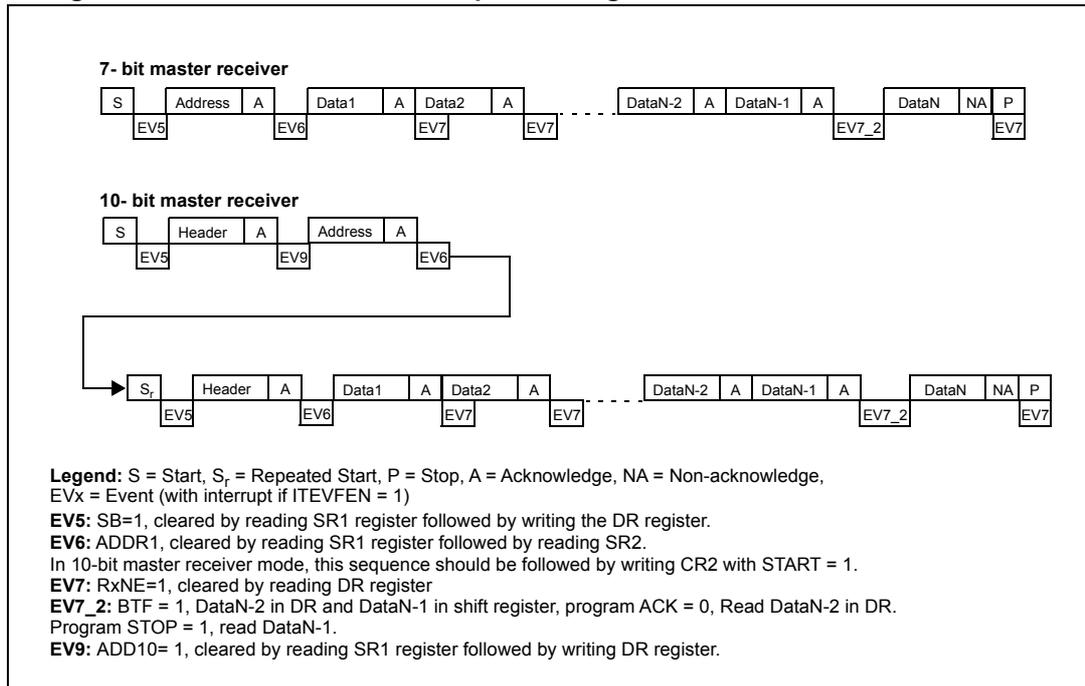
7- bit master receiver
| S | Address | A | Data1 | A | Data2 | A | ... | DataN-2 | A | DataN-1 | A | DataN | NA | P |
| EV5 | EV6 | EV7 | EV7 | EV7_2 |
10- bit master receiver
| S | Header | A | Address | A | ... | DataN-2 | A | DataN-1 | A | DataN | NA | P |
| EV5 | EV9 | EV6 | EV7_2 |
Legend:
S = Start, S
r
= Repeated Start, P = Stop, A = Acknowledge, NA = Non-acknowledge, EVx = Event (with interrupt if ITEVFEN = 1)
EV5:
SB=1, cleared by reading SR1 register followed by writing the DR register.
EV6:
ADDR1, cleared by reading SR1 register followed by reading SR2.
In 10-bit master receiver mode, this sequence should be followed by writing CR2 with START = 1.
EV7:
RxNE=1, cleared by reading DR register
EV7_2:
BTF = 1, DataN-2 in DR and DataN-1 in shift register, program ACK = 0, Read DataN-2 in DR.
Program STOP = 1, read DataN-1.
EV9:
ADD10= 1, cleared by reading SR1 register followed by writing DR register.
- 1. The EV5, EV6 and EV9 events stretch SCL low until the end of the corresponding software sequence.
- 2. The EV7 software sequence must complete before the end of the current byte transfer. In case EV7 software sequence can not be managed before the current byte end of transfer, it is recommended to use BTF instead of RXNE with the drawback of slowing the communication.
When 3 bytes remain to be read:
- • RxNE = 1 => Nothing (DataN-2 not read).
- • DataN-1 received
- • BTF = 1 because both shift and data registers are full: DataN-2 in DR and DataN-1 in the shift register => SCL tied low: no other data will be received on the bus.
- • Clear ACK bit
- • Read DataN-2 in DR => This will launch the DataN reception in the shift register
- • DataN received (with a NACK)
- • Program START/STOP
- • Read DataN-1
- • RxNE = 1
- • Read DataN
The procedure described above is valid for N>2. The cases where a single byte or two bytes are to be received should be handled differently, as described below:
- • Case of a single byte to be received:
- – In the ADDR event, clear the ACK bit.
- – Clear ADDR
- – Program the STOP/START bit.
- – Read the data after the RxNE flag is set.
- • Case of two bytes to be received:
- – Set POS and ACK
- – Wait for the ADDR flag to be set
- – Clear ADDR
- – Clear ACK
- – Wait for BTF to be set
- – Program STOP
- – Read DR twice
Figure 276. Method 2: transfer sequence diagram for master receiver when N=2
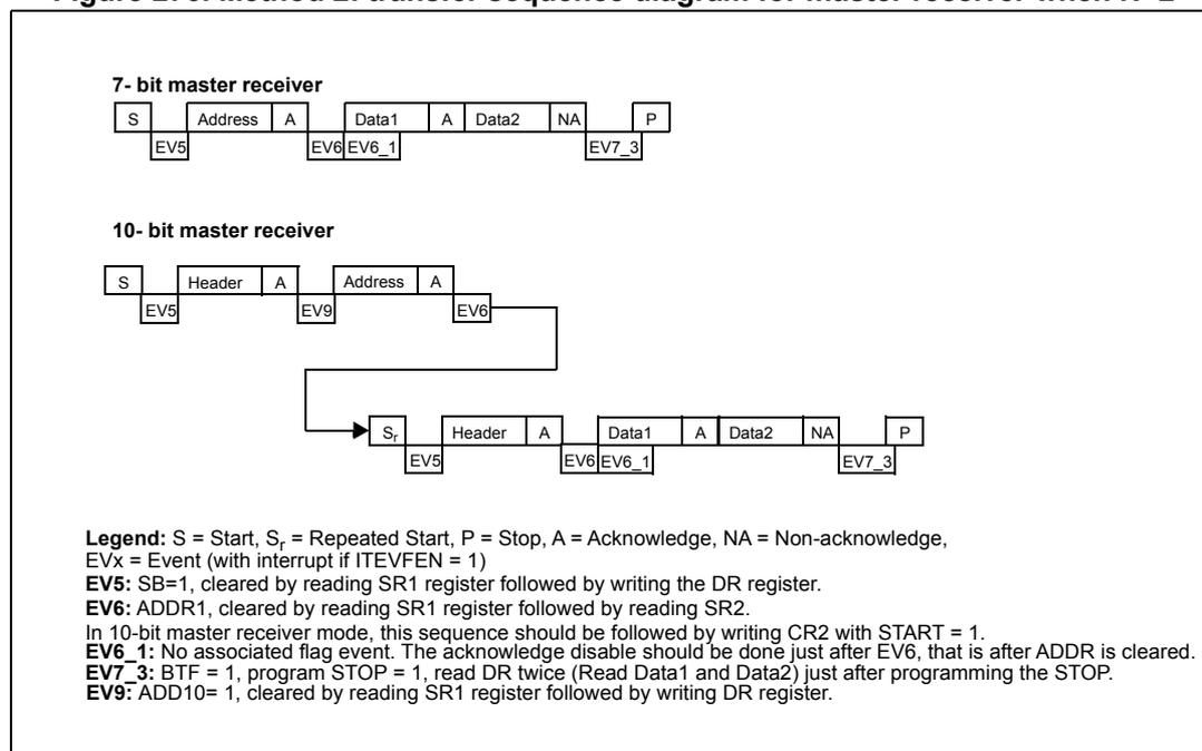
7- bit master receiver
| S | Address | A | Data1 | A | Data2 | NA | P |
| EV5 | EV6 | EV6_1 | EV7_3 |
10- bit master receiver
| S | Header | A | Address | A |
| EV5 | EV9 | EV6 |
→
| Sr | Header | A | Data1 | A | Data2 | NA | P |
| EV5 | EV6 | EV6_1 | EV7_3 |
Legend:
S = Start, Sr = Repeated Start, P = Stop, A = Acknowledge, NA = Non-acknowledge, EVx = Event (with interrupt if ITEVFEN = 1)
EV5:
SB=1, cleared by reading SR1 register followed by writing the DR register.
EV6:
ADDR1, cleared by reading SR1 register followed by reading SR2.
In 10-bit master receiver mode, this sequence should be followed by writing CR2 with START = 1.
EV6_1:
No associated flag event. The acknowledge disable should be done just after EV6, that is after ADDR is cleared.
EV7_3:
BTF = 1, program STOP = 1, read DR twice (Read Data1 and Data2) just after programming the STOP.
EV9:
ADD10= 1, cleared by reading SR1 register followed by writing DR register.
- 1. The EV5, EV6 and EV9 events stretch SCL low until the end of the corresponding software sequence.
- 2. The EV6_1 software sequence must complete before the ACK pulse of the current byte transfer.
Figure 277. Method 2: transfer sequence diagram for master receiver when N=1
7- bit master receiver
| S | Address | A | Data1 | NA | P |
| EV5 | EV6_3 | EV7 |
10- bit master receiver
| S | Header | A | Address | A |
| EV5 | EV9 | EV6 |
↳
| S r | Header | A | Data1 | NA | P |
| EV5 | EV6_3 | EV7 |
Legend:
S = Start, S
r
= Repeated Start, P = Stop, A = Acknowledge, NA = Non-acknowledge,
EVx = Event (with interrupt if ITEVFEN = 1)
EV5:
SB=1, cleared by reading SR1 register followed by writing the DR register.
EV6:
ADDR =1, cleared by reading SR1 register followed by reading SR2 register.
EV6_3:
ADDR = 1, program ACK = 0, clear ADDR by reading SR1 register followed by reading SR2 register, program STOP =1 just after ADDR is cleared.
Note:
The EV6_3 software sequence must complete before the current byte end of transfer.
EV7:
RxNE =1, cleared by reading DR register.
EV9:
ADD10= 1, cleared by reading SR1 register followed by writing DR register.
- 1. The EV5, EV6 and EV9 events stretch SCL low until the end of the corresponding software sequence.
26.3.4 Error conditions
The following are the error conditions which may cause communication to fail.
Bus error (BERR)
This error occurs when the I 2 C interface detects an external Stop or Start condition during an address or a data transfer. In this case:
- • the BERR bit is set and an interrupt is generated if the ITERREN bit is set
- • in Slave mode: data are discarded and the lines are released by hardware:
- – in case of a misplaced Start, the slave considers it is a restart and waits for an address, or a Stop condition
- – in case of a misplaced Stop, the slave behaves like for a Stop condition and the lines are released by hardware
- • In Master mode: the lines are not released and the state of the current transmission is not affected. It is up to the software to abort or not the current transmission
Acknowledge failure (AF)
This error occurs when the interface detects a nonacknowledge bit. In this case:
- • the AF bit is set and an interrupt is generated if the ITERREN bit is set
- • a transmitter which receives a NACK must reset the communication:
- – If Slave: lines are released by hardware
- – If Master: a Stop or repeated Start condition must be generated by software
Arbitration lost (ARLO)
This error occurs when the I 2 C interface detects an arbitration lost condition. In this case
- • the ARLO bit is set by hardware (and an interrupt is generated if the ITERREN bit is set)
- • the I 2 C Interface goes automatically back to slave mode (the MSL bit is cleared). When the I 2 C loses the arbitration, it is not able to acknowledge its slave address in the same transfer, but it can acknowledge it after a repeated Start from the winning master.
- • lines are released by hardware
Overrun/underrun error (OVR)
An overrun error can occur in slave mode when clock stretching is disabled and the I 2 C interface is receiving data. The interface has received a byte (RxNE=1) and the data in DR has not been read, before the next byte is received by the interface. In this case,
- • The last received byte is lost.
- • In case of Overrun error, software should clear the RxNE bit and the transmitter should re-transmit the last received byte.
Underrun error can occur in slave mode when clock stretching is disabled and the I 2 C interface is transmitting data. The interface has not updated the DR with the next byte (TxE=1), before the clock comes for the next byte. In this case,
- • The same byte in the DR register will be sent again
- • The user should make sure that data received on the receiver side during an underrun error are discarded and that the next bytes are written within the clock low time specified in the I 2 C bus standard.
For the first byte to be transmitted, the DR must be written after ADDR is cleared and before the first SCL rising edge. If not possible, the receiver must discard the first data.
26.3.5 SDA/SCL line control
- • If clock stretching is enabled:
- – Transmitter mode: If TxE=1 and BTF=1: the interface holds the clock line low before transmission to wait for the microcontroller to read SR1 and then write the byte in the Data register (both buffer and shift register are empty).
- – Receiver mode: If RxNE=1 and BTF=1: the interface holds the clock line low after reception to wait for the microcontroller to read SR1 and then read the byte in the Data register (both buffer and shift register are full).
- • If clock stretching is disabled in Slave mode:
- – Overrun Error in case of RxNE=1 and no read of DR has been done before the next byte is received. The last received byte is lost.
- – Underrun Error in case TxE=1 and no write into DR has been done before the next byte must be transmitted. The same byte will be sent again.
- – Write Collision not managed.
26.3.6 SMBus
Introduction
The System Management Bus (SMBus) is a two-wire interface through which various devices can communicate with each other and with the rest of the system. It is based on I 2 C principles of operation. SMBus provides a control bus for system and power management related tasks. A system may use SMBus to pass messages to and from devices instead of toggling individual control lines.
The System Management Bus Specification refers to three types of devices. A slave is a device that is receiving or responding to a command. A master is a device that issues commands, generates the clocks, and terminates the transfer. A host is a specialized master that provides the main interface to the system's CPU. A host must be a master-slave and must support the SMBus host notify protocol. Only one host is allowed in a system.
Similarities between SMBus and I 2 C
- • 2-wire bus protocol (1 Clk, 1 Data) + SMBus Alert line optional
- • Master-slave communication, Master provides clock
- • Multi master capability
- • SMBus data format similar to I 2 C 7-bit addressing format ( Figure 269 ).
Differences between SMBus and I 2 C
The following table describes the differences between SMBus and I 2 C.
Table 188. SMBus vs. I 2 C
| SMBus | I 2 C |
|---|---|
| Max. speed 100 kHz | Max. speed 400 kHz |
| Min. clock speed 10 kHz | No minimum clock speed |
| 35 ms clock low timeout | No timeout |
| Logic levels are fixed | Logic levels are V DD dependent |
| Different address types (reserved, dynamic etc.) | 7-bit, 10-bit and general call slave address types |
| Different bus protocols (quick command, process call etc.) | No bus protocols |
SMBus application usage
With System Management Bus, a device can provide manufacturer information, tell the system what its model/part number is, save its state for a suspend event, report different types of errors, accept control parameters, and return its status. SMBus provides a control bus for system and power management related tasks.
Device identification
Any device that exists on the System Management Bus as a slave has a unique address called the Slave Address. For the list of reserved slave addresses, refer to the SMBus specification version. 2.0 ( http://smbus.org/ ).
Bus protocols
The SMBus specification supports up to nine bus protocols. For more details of these protocols and SMBus address types, refer to SMBus specification version. 2.0. These protocols should be implemented by the user software.
Address resolution protocol (ARP)
SMBus slave address conflicts can be resolved by dynamically assigning a new unique address to each slave device. The Address Resolution Protocol (ARP) has the following attributes:
- • Address assignment uses the standard SMBus physical layer arbitration mechanism
- • Assigned addresses remain constant while device power is applied; address retention through device power loss is also allowed
- • No additional SMBus packet overhead is incurred after address assignment. (i.e. subsequent accesses to assigned slave addresses have the same overhead as accesses to fixed address devices.)
- • Any SMBus master can enumerate the bus
Unique device identifier (UDID)
In order to provide a mechanism to isolate each device for the purpose of address assignment, each device must implement a unique device identifier (UDID).
For the details on 128-bit UDID and more information on ARP, refer to SMBus specification version 2.0.
SMBus alert mode
SMBus Alert is an optional signal with an interrupt line for devices that want to trade their ability to master for a pin. SMBA is a wired-AND signal just as the SCL and SDA signals are. SMBA is used in conjunction with the SMBus General Call Address. Messages invoked with the SMBus are two bytes long.
A slave-only device can signal the host through SMBA that it wants to talk by setting ALERT bit in I2C_CR1 register. The host processes the interrupt and simultaneously accesses all SMBA devices through the Alert Response Address (known as ARA having a value 0001 100X). Only the device(s) which pulled SMBA low will acknowledge the Alert Response Address. This status is identified using SMBALERT Status flag in I2C_SR1 register. The host performs a modified Receive Byte operation. The 7 bit device address provided by the slave transmit device is placed in the 7 most significant bits of the byte. The eighth bit can be a zero or one.
If more than one device pulls SMBA low, the highest priority (lowest address) device will win communication rights via standard arbitration during the slave address transfer. After acknowledging the slave address the device must disengage its SMBA pull-down. If the host still sees SMBA low when the message transfer is complete, it knows to read the ARA again.
A host which does not implement the SMBA signal may periodically access the ARA.
For more details on SMBus Alert mode, refer to SMBus specification version 2.0.
Timeout error
There are differences in the timing specifications between I 2 C and SMBus. SMBus defines a clock low timeout, TIMEOUT of 35 ms. Also SMBus specifies TLOW:
SEXT as the cumulative clock low extend time for a slave device. SMBus specifies TLOW: MEXT as the cumulative clock low extend time for a master device. For more details on these timeouts, refer to SMBus specification version 2.0.
The status flag Timeout or Tlow Error in I2C_SR1 shows the status of this feature.
How to use the interface in SMBus mode
To switch from I 2 C mode to SMBus mode, the following sequence should be performed.
- • Set the SMBus bit in the I2C_CR1 register
- • Configure the SMBTYPE and ENARP bits in the I2C_CR1 register as required for the application
If you want to configure the device as a master, follow the Start condition generation procedure in Section 26.3.3 . Otherwise, follow the sequence in Section 26.3.2 .
The application has to control the various SMBus protocols by software.
- • SMB Device Default Address acknowledged if ENARP=1 and SMBTYPE=0
- • SMB Host Header acknowledged if ENARP=1 and SMBTYPE=1
- • SMB Alert Response Address acknowledged if SMBALERT=1
26.3.7 DMA requests
DMA requests (when enabled) are generated only for data transfer. DMA requests are generated by Data register becoming empty in transmission and Data register becoming full in reception. The DMA must be initialized and enabled before the I2C data transfer. The DMAEN bit must be set in the I2C_CR2 register before the ADDR event. In master mode or in slave mode when clock stretching is enabled, the DMAEN bit can also be set during the ADDR event, before clearing the ADDR flag. The DMA request must be served before the end of the current byte transfer. When the number of data transfers which has been programmed for the corresponding DMA stream is reached, the DMA controller sends an End of Transfer EOT signal to the I 2 C interface and generates a Transfer Complete interrupt if enabled:
- • Master transmitter: In the interrupt routine after the EOT interrupt, disable DMA requests then wait for a BTF event before programming the Stop condition.
- • Master receiver: when the number of bytes to be received is equal to or greater than two, the DMA controller sends a hardware signal, EOT_1, corresponding to the last but one data byte (number_of_bytes – 1). If, in the I2C_CR2 register, the LAST bit is set, I 2 C automatically sends a NACK after the next byte following EOT_1. The user can generate a Stop condition in the DMA Transfer Complete interrupt routine if enabled.
Transmission using DMA
DMA mode can be enabled for transmission by setting the DMAEN bit in the I2C_CR2 register. Data will be loaded from a Memory area configured using the DMA peripheral (refer to the DMA specification) to the I2C_DR register whenever the TxE bit is set. To map a DMA stream x for I 2 C transmission (where x is the stream number), perform the following sequence:
- 1. Set the I2C_DR register address in the DMA_SxPAR register. The data will be moved to this address from the memory after each TxE event.
- 2. Set the memory address in the DMA_SxMA0R register (and in DMA_SxMA1R register in the case of a double buffer mode). The data will be loaded into I2C_DR from this memory after each TxE event.
- 3. Configure the total number of bytes to be transferred in the DMA_SxNDTR register. After each TxE event, this value will be decremented.
- 4. Configure the DMA stream priority using the PL[0:1] bits in the DMA_SxCR register
- 5. Set the DIR bit in the DMA_SxCR register and configure interrupts after half transfer or full transfer depending on application requirements.
- 6. Activate the stream by setting the EN bit in the DMA_SxCR register.
When the number of data transfers which has been programmed in the DMA Controller registers is reached, the DMA controller sends an End of Transfer EOT/ EOT_1 signal to the I 2 C interface and the DMA generates an interrupt, if enabled, on the DMA stream interrupt vector.
Note: Do not enable the ITBUFEN bit in the I2C_CR2 register if DMA is used for transmission.
Reception using DMA
DMA mode can be enabled for reception by setting the DMAEN bit in the I2C_CR2 register. Data will be loaded from the I2C_DR register to a Memory area configured using the DMA peripheral (refer to the DMA specification) whenever a data byte is received. To map a DMA stream x for I 2 C reception (where x is the stream number), perform the following sequence:
- 1. Set the I2C_DR register address in DMA_SxPAR register. The data will be moved from this address to the memory after each RxNE event.
- 2. Set the memory address in the DMA_SxMA0R register (and in DMA_SxMA1R register in the case of a double buffer mode). The data will be loaded from the I2C_DR register to this memory area after each RxNE event.
- 3. Configure the total number of bytes to be transferred in the DMA_SxNDTR register. After each RxNE event, this value will be decremented.
- 4. Configure the stream priority using the PL[0:1] bits in the DMA_SxCR register
- 5. Reset the DIR bit and configure interrupts in the DMA_SxCR register after half transfer or full transfer depending on application requirements.
- 6. Activate the stream by setting the EN bit in the DMA_SxCR register.
When the number of data transfers which has been programmed in the DMA Controller registers is reached, the DMA controller sends an End of Transfer EOT/ EOT_1 signal to the I 2 C interface and DMA generates an interrupt, if enabled, on the DMA stream interrupt vector.
Note: Do not enable the ITBUFEN bit in the I2C_CR2 register if DMA is used for reception.
26.3.8 Packet error checking
A PEC calculator has been implemented to improve the reliability of communication. The PEC is calculated by using the \( C(x) = x^8 + x^2 + x + 1 \) CRC-8 polynomial serially on each bit.
- • PEC calculation is enabled by setting the ENPEC bit in the I2C_CR1 register. PEC is a CRC-8 calculated on all message bytes including addresses and R/W bits.
- – In transmission: set the PEC transfer bit in the I2C_CR1 register after the TxE event corresponding to the last byte. The PEC will be transferred after the last transmitted byte.
- – In reception: set the PEC bit in the I2C_CR1 register after the RxNE event corresponding to the last byte so that the receiver sends a NACK if the next received byte is not equal to the internally calculated PEC. In case of Master-Receiver, a NACK must follow the PEC whatever the check result. The PEC must be set before the ACK pulse of the current byte reception.
- • A PECERR error flag/interrupt is also available in the I2C_SR1 register.
- • If DMA and PEC calculation are both enabled:-
- – In transmission: when the I 2 C interface receives an EOT signal from the DMA controller, it automatically sends a PEC after the last byte.
- – In reception: when the I 2 C interface receives an EOT_1 signal from the DMA controller, it will automatically consider the next byte as a PEC and will check it. A DMA request is generated after PEC reception.
- • To allow intermediate PEC transfers, a control bit is available in the I2C_CR2 register (LAST bit) to determine if it is really the last DMA transfer or not. If it is the last DMA request for a master receiver, a NACK is automatically sent after the last received byte.
- • PEC calculation is corrupted by an arbitration loss.
26.4 I 2 C interrupts
The table below gives the list of I 2 C interrupt requests.
Table 189. I 2 C Interrupt requests
| Interrupt event | Event flag | Enable control bit |
|---|---|---|
| Start bit sent (Master) | SB | ITEVFEN |
| Address sent (Master) or Address matched (Slave) | ADDR | |
| 10-bit header sent (Master) | ADD10 | |
| Stop received (Slave) | STOPF | |
| Data byte transfer finished | BTF | |
| Receive buffer not empty | RxNE | ITEVFEN and ITBUFEN |
| Transmit buffer empty | TxE |
| Interrupt event | Event flag | Enable control bit |
|---|---|---|
| Bus error | BERR | ITERREN |
| Arbitration loss (Master) | ARLO | |
| Acknowledge failure | AF | |
| Overrun/Underrun | OVR | |
| PEC error | PECERR | |
| Timeout/Tlow error | TIMEOUT | |
| SMBus Alert | SMBALERT |
Note: SB, ADDR, ADD10, STOPF, BTF, RxNE and TxE are logically OR-ed on the same interrupt channel.
BERR, ARLO, AF, OVR, PECERR, TIMEOUT and SMBALERT are logically OR-ed on the same interrupt channel.
Figure 278. I 2 C interrupt mapping diagram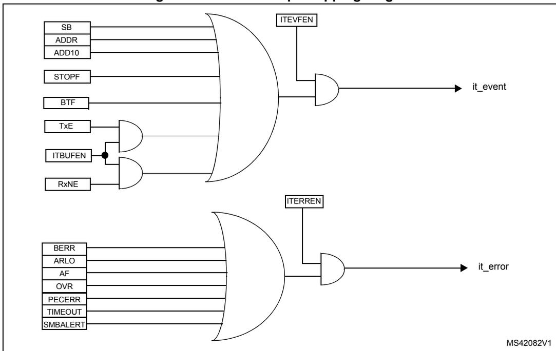
The diagram illustrates the logic for generating I 2 C interrupt signals. It consists of two main parts:
- it_event channel: This channel is active when the ITEVFEN bit is set and any of the following conditions are met: SB (Start), ADDR (Address), ADD10 (10-bit address), STOPF (Stop), BTF (Byte Transfer Finished), or a combination of TxE (Transmit Buffer Empty), ITBUFEN (Interrupt Buffer Enable), and RxNE (Receive Buffer Not Empty).
- it_error channel: This channel is active when the ITERREN bit is set and any of the following error conditions are met: BERR (Bus Error), ARLO (Arbitration Loss), AF (Acknowledge Failure), OVR (Overrun/Underrun), PECERR (PEC Error), TIMEOUT (Timeout/Tlow Error), or SMBALERT (SMBus Alert).
MS42082V1
26.5 I 2 C debug mode
When the microcontroller enters the debug mode (Cortex ® -M3 core halted), the SMBUS timeout either continues to work normally or stops, depending on the DBG_I2Cx_SMBUS_TIMEOUT configuration bits in the DBG module. For more details, refer to Section 31.16.2: Debug support for timers, watchdog, bxCAN and I 2 C .
26.6 I 2 C registers
Refer to for a list of abbreviations used in register descriptions.
The peripheral registers have to be accessed by half-words (16 bits) or words (32 bits).
26.6.1 I 2 C Control register 1 (I2C_CR1)
Address offset: 0x00
Reset value: 0x0000
| 15 | 14 | 13 | 12 | 11 | 10 | 9 | 8 | 7 | 6 | 5 | 4 | 3 | 2 | 1 | 0 |
|---|---|---|---|---|---|---|---|---|---|---|---|---|---|---|---|
| SWRST | Res. | ALERT | PEC | POS | ACK | STOP | START | NO STRETCH | ENGCC | ENPEC | ENARP | SMB TYPE | Res. | SMBUS | PE |
| rw | rw | rw | rw | rw | rw | rw | rw | rw | rw | rw | rw | rw | rw |
Bit 15 SWRST : Software reset
When set, the I2C is under reset state. Before resetting this bit, make sure the I2C lines are released and the bus is free.
0: I 2 C Peripheral not under reset
1: I 2 C Peripheral under reset state
Note: This bit can be used to reinitialize the peripheral after an error or a locked state. As an example, if the BUSY bit is set and remains locked due to a glitch on the bus, the SWRST bit can be used to exit from this state.
Bit 14 Reserved, must be kept at reset value
Bit 13 ALERT : SMBus alert
This bit is set and cleared by software, and cleared by hardware when PE=0.
0: Releases SMBA pin high. Alert Response Address Header followed by NACK.
1: Drives SMBA pin low. Alert Response Address Header followed by ACK.
Bit 12 PEC : Packet error checking
This bit is set and cleared by software, and cleared by hardware when PEC is transferred or by a START or Stop condition or when PE=0.
0: No PEC transfer
1: PEC transfer (in Tx or Rx mode)
Note: PEC calculation is corrupted by an arbitration loss.
Bit 11 POS : Acknowledge/PEC Position (for data reception)
This bit is set and cleared by software and cleared by hardware when PE=0.
0: ACK bit controls the (N)ACK of the current byte being received in the shift register. The PEC bit indicates that current byte in shift register is a PEC.
1: ACK bit controls the (N)ACK of the next byte which will be received in the shift register. The PEC bit indicates that the next byte in the shift register is a PEC
Note: The POS bit is used when the procedure for reception of 2 bytes (see Method 2: transfer sequence diagram for master receiver when N=2 ) is followed. It must be configured before data reception starts. In this case, to NACK the 2nd byte, the ACK bit must be cleared just after ADDR is cleared. To check the 2nd byte as PEC, the PEC bit must be set during the ADDR stretch event after configuring the POS bit.
Bit 10 ACK : Acknowledge enable
This bit is set and cleared by software and cleared by hardware when PE=0.
0: No acknowledge returned
1: Acknowledge returned after a byte is received (matched address or data)
Bit 9 STOP : Stop generation
The bit is set and cleared by software, cleared by hardware when a Stop condition is detected, set by hardware when a timeout error is detected.
In Master Mode:
0: No Stop generation.
1: Stop generation after the current byte transfer or after the current Start condition is sent.
In Slave mode:
0: No Stop generation.
1: Release the SCL and SDA lines after the current byte transfer.
Bit 8 START : Start generation
This bit is set and cleared by software and cleared by hardware when start is sent or PE=0.
In Master Mode:
0: No Start generation
1: Repeated start generation
In Slave mode:
0: No Start generation
1: Start generation when the bus is free
Bit 7 NOSTRETCH : Clock stretching disable (Slave mode)
This bit is used to disable clock stretching in slave mode when ADDR or BTF flag is set, until it is reset by software.
0: Clock stretching enabled
1: Clock stretching disabled
Bit 6 ENGCG : General call enable
0: General call disabled. Address 00h is NACKed.
1: General call enabled. Address 00h is ACKed.
Bit 5 ENPEC : PEC enable
0: PEC calculation disabled
1: PEC calculation enabled
Bit 4 ENARP : ARP enable
0: ARP disable
1: ARP enable
SMBus Device default address recognized if SMBTYPE=0
SMBus Host address recognized if SMBTYPE=1
Bit 3 SMBTYPE : SMBus type
0: SMBus Device
1: SMBus Host
Bit 2 Reserved, must be kept at reset value
Bit 1 SMBUS : SMBus mode
0: I 2 C mode
1: SMBus mode
Bit 0 PE : Peripheral enable
0: Peripheral disable
1: Peripheral enable
Note: If this bit is reset while a communication is on going, the peripheral is disabled at the end of the current communication, when back to IDLE state.
All bit resets due to PE=0 occur at the end of the communication.
In master mode, this bit must not be reset before the end of the communication.
Note: When the STOP, START or PEC bit is set, the software must not perform any write access to I2C_CR1 before this bit is cleared by hardware. Otherwise there is a risk of setting a second STOP, START or PEC request.
26.6.2 I 2 C Control register 2 (I2C_CR2)
Address offset: 0x04
Reset value: 0x0000
| 15 | 14 | 13 | 12 | 11 | 10 | 9 | 8 | 7 | 6 | 5 | 4 | 3 | 2 | 1 | 0 |
|---|---|---|---|---|---|---|---|---|---|---|---|---|---|---|---|
| Reserved | LAST | DMAEN | ITBUFEN | ITEVTEN | ITERREN | Reserved | FREQ[5:0] | ||||||||
| rw | rw | rw | rw | rw | rw | rw | rw | rw | rw | rw | |||||
Bits 15:13 Reserved, must be kept at reset value
Bit 12 LAST : DMA last transfer
0: Next DMA EOT is not the last transfer
1: Next DMA EOT is the last transfer
Note: This bit is used in master receiver mode to permit the generation of a NACK on the last received data.
Bit 11 DMAEN : DMA requests enable
0: DMA requests disabled
1: DMA request enabled when TxE=1 or RxNE =1
Bit 10 ITBUFEN : Buffer interrupt enable
0: TxE = 1 or RxNE = 1 does not generate any interrupt.
1: TxE = 1 or RxNE = 1 generates Event Interrupt (whatever the state of DMAEN)
Bit 9 ITEVTEN: Event interrupt enable0: Event interrupt disabled
1: Event interrupt enabled
This interrupt is generated when:
- – SB = 1 (Master)
- – ADDR = 1 (Master/Slave)
- – ADD10= 1 (Master)
- – STOPF = 1 (Slave)
- – BTF = 1 with no TxE or RxNE event
- – TxE event to 1 if ITBUFEN = 1
- – RxNE event to 1 if ITBUFEN = 1
0: Error interrupt disabled
1: Error interrupt enabled
This interrupt is generated when:
- – BERR = 1
- – ARLO = 1
- – AF = 1
- – OVR = 1
- – PECERR = 1
- – TIMEOUT = 1
- – SMBALERT = 1
Bits 7:6 Reserved, must be kept at reset value
Bits 5:0 FREQ[5:0]: Peripheral clock frequencyThe FREQ bits must be configured with the APB clock frequency value (I2C peripheral connected to APB). The FREQ field is used by the peripheral to generate data setup and hold times compliant with the I2C specifications. The minimum allowed frequency is 2 MHz, the maximum frequency is limited by the maximum APB frequency and cannot exceed 50 MHz (peripheral intrinsic maximum limit).
0b000000: Not allowed
0b000001: Not allowed
0b000010: 2 MHz
...
0b110010: 50 MHz
Higher than 0b101010: Not allowed
26.6.3 I 2 C Own address register 1 (I2C_OAR1)
Address offset: 0x08
Reset value: 0x0000
| 15 | 14 | 13 | 12 | 11 | 10 | 9 | 8 | 7 | 6 | 5 | 4 | 3 | 2 | 1 | 0 |
|---|---|---|---|---|---|---|---|---|---|---|---|---|---|---|---|
| ADD MODE | Reserved | ADD[9:8] | ADD[7:1] | ADD0 | |||||||||||
| rw | rw | rw | rw | rw | rw | rw | rw | rw | rw | rw | |||||
Bit 15 ADDMODE : Addressing mode (slave mode)
0: 7-bit slave address (10-bit address not acknowledged)
1: 10-bit slave address (7-bit address not acknowledged)
Bit 14: Should always be kept at 1 by software.
Bits 13:10: Reserved, must be kept at reset value
Bits 9:8 ADD[9:8] : Interface address
7-bit addressing mode: don't care
10-bit addressing mode: bits 9:8 of address
Bits 7:1 ADD[7:1] : Interface address
bits 7:1 of address
Bit 0 ADD0 : Interface address
7-bit addressing mode: don't care
10-bit addressing mode: bit 0 of address
26.6.4 I 2 C Own address register 2 (I2C_OAR2)
Address offset: 0x0C
Reset value: 0x0000
| 15 | 14 | 13 | 12 | 11 | 10 | 9 | 8 | 7 | 6 | 5 | 4 | 3 | 2 | 1 | 0 |
|---|---|---|---|---|---|---|---|---|---|---|---|---|---|---|---|
| Reserved | ADD2[7:1] | ENDUAL | |||||||||||||
| rw | rw | rw | rw | rw | rw | rw | rw | ||||||||
Bits 15:8: Reserved, must be kept at reset value
Bits 7:1 ADD2[7:1] : Interface address
bits 7:1 of address in dual addressing mode
Bit 0 ENDUAL : Dual addressing mode enable
0: Only OAR1 is recognized in 7-bit addressing mode
1: Both OAR1 and OAR2 are recognized in 7-bit addressing mode
26.6.5 I 2 C Data register (I2C_DR)
Address offset: 0x10
Reset value: 0x0000
| 15 | 14 | 13 | 12 | 11 | 10 | 9 | 8 | 7 | 6 | 5 | 4 | 3 | 2 | 1 | 0 |
|---|---|---|---|---|---|---|---|---|---|---|---|---|---|---|---|
| Reserved | DR[7:0] | ||||||||||||||
| rw | rw | rw | rw | rw | rw | rw | rw | ||||||||
Bits 15:8 Reserved, must be kept at reset value
Bits 7:0 DR[7:0] 8-bit data register
Byte received or to be transmitted to the bus.
- – Transmitter mode: Byte transmission starts automatically when a byte is written in the DR register. A continuous transmit stream can be maintained if the next data to be transmitted is put in DR once the transmission is started (TxE=1)
- – Receiver mode: Received byte is copied into DR (RxNE=1). A continuous transmit stream can be maintained if DR is read before the next data byte is received (RxNE=1).
Note: In slave mode, the address is not copied into DR.
Write collision is not managed (DR can be written if TxE=0).
If an ARLO event occurs on ACK pulse, the received byte is not copied into DR and so cannot be read.
26.6.6 I 2 C Status register 1 (I2C_SR1)
Address offset: 0x14
Reset value: 0x0000
| 15 | 14 | 13 | 12 | 11 | 10 | 9 | 8 | 7 | 6 | 5 | 4 | 3 | 2 | 1 | 0 |
|---|---|---|---|---|---|---|---|---|---|---|---|---|---|---|---|
| SMB ALERT | TIME OUT | Res. | PEC ERR | OVR | AF | ARLO | BERR | TxE | RxNE | Res. | STOPF | ADD10 | BTF | ADDR | SB |
| rc_w0 | rc_w0 | rc_w0 | rc_w0 | rc_w0 | rc_w0 | rc_w0 | r | r | r | r | r | r | r |
Bit 15 SMBALERT : SMBus alert
In SMBus host mode:
0: no SMBALERT
1: SMBALERT event occurred on pin
In SMBus slave mode:
0: no SMBALERT response address header
1: SMBALERT response address header to SMBALERT LOW received
- – Cleared by software writing 0, or by hardware when PE=0.
Bit 14 TIMEOUT : Timeout or Tlow error
0: No timeout error
1: SCL remained LOW for 25 ms (Timeout)
or
Master cumulative clock low extend time more than 10 ms (Tlow:mext)
or
Slave cumulative clock low extend time more than 25 ms (Tlow:sext)
- – When set in slave mode: slave resets the communication and lines are released by hardware
- – When set in master mode: Stop condition sent by hardware
- – Cleared by software writing 0, or by hardware when PE=0.
Note: This functionality is available only in SMBus mode.
Bit 13 Reserved, must be kept at reset value
Bit 12 PECERR : PEC Error in reception
0: no PEC error: receiver returns ACK after PEC reception (if ACK=1)
1: PEC error: receiver returns NACK after PEC reception (whatever ACK)
Note: Cleared by software writing 0, or by hardware when PE=0.
Bit 11 OVR : Overrun/Underrun
0: No overrun/underrun
1: Overrun or underrun
- – Set by hardware in slave mode when NOSTRETCH=1 and:
- – In reception when a new byte is received (including ACK pulse) and the DR register has not been read yet. New received byte is lost.
- – In transmission when a new byte should be sent and the DR register has not been written yet. The same byte is sent twice.
- – Cleared by software writing 0, or by hardware when PE=0.
Note: If the DR write occurs very close to SCL rising edge, the sent data is unspecified and a hold timing error occurs
Bit 10 AF : Acknowledge failure
0: No acknowledge failure
1: Acknowledge failure
- – Set by hardware when no acknowledge is returned.
- – Cleared by software writing 0, or by hardware when PE=0.
Bit 9 ARLO : Arbitration lost (master mode)
0: No Arbitration Lost detected
1: Arbitration Lost detected
Set by hardware when the interface loses the arbitration of the bus to another master
- – Cleared by software writing 0, or by hardware when PE=0.
After an ARLO event the interface switches back automatically to Slave mode (MSL=0).
Note: In SMBUS, the arbitration on the data in slave mode occurs only during the data phase, or the acknowledge transmission (not on the address acknowledge).
Bit 8 BERR : Bus error
0: No misplaced Start or Stop condition
1: Misplaced Start or Stop condition
- – Set by hardware when the interface detects an SDA rising or falling edge while SCL is high, occurring in a non-valid position during a byte transfer.
- – Cleared by software writing 0, or by hardware when PE=0.
Bit 7 TxE : Data register empty (transmitters)
0: Data register not empty
1: Data register empty
- – Set when DR is empty in transmission. TxE is not set during address phase.
- – Cleared by software writing to the DR register or by hardware after a start or a stop condition or when PE=0.
TxE is not set if either a NACK is received, or if next byte to be transmitted is PEC (PEC=1)
Note: TxE is not cleared by writing the first data being transmitted, or by writing data when BTF is set, as in both cases the data register is still empty.
Bit 6 RxNE : Data register not empty (receivers)
0: Data register empty
1: Data register not empty
- – Set when data register is not empty in receiver mode. RxNE is not set during address phase.
- – Cleared by software reading or writing the DR register or by hardware when PE=0.
RxNE is not set in case of ARLO event.
Note: RxNE is not cleared by reading data when BTF is set, as the data register is still full.
Bit 5 Reserved, must be kept at reset value
Bit 4 STOPF : Stop detection (slave mode)
0: No Stop condition detected
1: Stop condition detected
- – Set by hardware when a Stop condition is detected on the bus by the slave after an acknowledge (if ACK=1).
- – Cleared by software reading the SR1 register followed by a write in the CR1 register, or by hardware when PE=0
Note: The STOPF bit is not set after a NACK reception.
It is recommended to perform the complete clearing sequence (READ SR1 then WRITE CR1) after the STOPF is set. Refer to Figure 272.
Bit 3 ADD10 : 10-bit header sent (Master mode)
0: No ADD10 event occurred.
1: Master has sent first address byte (header).
- – Set by hardware when the master has sent the first byte in 10-bit address mode.
- – Cleared by software reading the SR1 register followed by a write in the DR register of the second address byte, or by hardware when PE=0.
Note: ADD10 bit is not set after a NACK reception
Bit 2 BTF : Byte transfer finished
0: Data byte transfer not done
1: Data byte transfer succeeded
- – Set by hardware when NOSTRETCH=0 and:
- – In reception when a new byte is received (including ACK pulse) and DR has not been read yet (RxNE=1).
- – In transmission when a new byte should be sent and DR has not been written yet (TxE=1).
- – Cleared by software reading SR1 followed by either a read or write in the DR register or by hardware after a start or a stop condition in transmission or when PE=0.
Note: The BTF bit is not set after a NACK reception
The BTF bit is not set if next byte to be transmitted is the PEC (TRA=1 in I2C_SR2 register and PEC=1 in I2C_CR1 register)
Bit 1 ADDR : Address sent (master mode)/matched (slave mode)
This bit is cleared by software reading SR1 register followed reading SR2, or by hardware when PE=0.
Address matched (Slave)
0: Address mismatched or not received.
1: Received address matched.
- – Set by hardware as soon as the received slave address matched with the OAR registers content or a general call or a SMBus Device Default Address or SMBus Host or SMBus Alert is recognized. (when enabled depending on configuration).
Note: In slave mode, it is recommended to perform the complete clearing sequence (READ SR1 then READ SR2) after ADDR is set. Refer to Figure 272.
Address sent (Master)
0: No end of address transmission
1: End of address transmission
- – For 10-bit addressing, the bit is set after the ACK of the 2nd byte.
- – For 7-bit addressing, the bit is set after the ACK of the byte.
Note: ADDR is not set after a NACK reception
Bit 0 SB : Start bit (Master mode)
0: No Start condition
1: Start condition generated.
- – Set when a Start condition generated.
- – Cleared by software by reading the SR1 register followed by writing the DR register, or by hardware when PE=0
26.6.7 I 2 C Status register 2 (I2C_SR2)
Address offset: 0x18
Reset value: 0x0000
Note: Reading I2C_SR2 after reading I2C_SR1 clears the ADDR flag, even if the ADDR flag was set after reading I2C_SR1. Consequently, I2C_SR2 must be read only when ADDR is found set in I2C_SR1 or when the STOPF bit is cleared.
| 15 | 14 | 13 | 12 | 11 | 10 | 9 | 8 | 7 | 6 | 5 | 4 | 3 | 2 | 1 | 0 |
|---|---|---|---|---|---|---|---|---|---|---|---|---|---|---|---|
| PEC[7:0] | DUALF | SMB HOST | SMBDE FAULT | GEN CALL | Res. | TRA | BUSY | MSL | |||||||
| r | r | r | r | r | r | r | r | r | r | r | r | r | r | r | |
Bits 15:8 PEC[7:0] Packet error checking register
This register contains the internal PEC when ENPEC=1.
Bit 7 DUALF : Dual flag (Slave mode)
0: Received address matched with OAR1
1: Received address matched with OAR2
- – Cleared by hardware after a Stop condition or repeated Start condition, or when PE=0.
Bit 6 SMBHOST : SMBus host header (Slave mode)
0: No SMBus Host address
1: SMBus Host address received when SMBTYPE=1 and ENARP=1.
- – Cleared by hardware after a Stop condition or repeated Start condition, or when PE=0.
Bit 5 SMBDEFAULT : SMBus device default address (Slave mode)
0: No SMBus Device Default address
1: SMBus Device Default address received when ENARP=1
– Cleared by hardware after a Stop condition or repeated Start condition, or when PE=0.
Bit 4 GENCALL : General call address (Slave mode)
0: No General Call
1: General Call Address received when ENGCG=1
– Cleared by hardware after a Stop condition or repeated Start condition, or when PE=0.
Bit 3 Reserved, must be kept at reset value
Bit 2 TRA : Transmitter/receiver
0: Data bytes received
1: Data bytes transmitted
This bit is set depending on the R/W bit of the address byte, at the end of total address phase.
It is also cleared by hardware after detection of Stop condition (STOPF=1), repeated Start condition, loss of bus arbitration (ARLO=1), or when PE=0.
Bit 1 BUSY : Bus busy
0: No communication on the bus
1: Communication ongoing on the bus
– Set by hardware on detection of SDA or SCL low
– cleared by hardware on detection of a Stop condition.
It indicates a communication in progress on the bus. This information is still updated when the interface is disabled (PE=0).
Bit 0 MSL : Master/slave
0: Slave Mode
1: Master Mode
– Set by hardware as soon as the interface is in Master mode (SB=1).
– Cleared by hardware after detecting a Stop condition on the bus or a loss of arbitration (ARLO=1), or by hardware when PE=0.
Note: Reading I2C_SR2 after reading I2C_SR1 clears the ADDR flag, even if the ADDR flag was set after reading I2C_SR1. Consequently, I2C_SR2 must be read only when ADDR is found set in I2C_SR1 or when the STOPF bit is cleared.
26.6.8 I 2 C Clock control register (I2C_CCR)
Address offset: 0x1C
Reset value: 0x0000
Note: f PCLK1 must be at least 2 MHz to achieve Sm mode I 2 C frequencies. It must be at least 4 MHz to achieve Fm mode I 2 C frequencies. It must be a multiple of 10MHz to reach the 400 kHz maximum I 2 C Fm mode clock.
The CCR register must be configured only when the I2C is disabled (PE = 0).
| 15 | 14 | 13 | 12 | 11 | 10 | 9 | 8 | 7 | 6 | 5 | 4 | 3 | 2 | 1 | 0 |
|---|---|---|---|---|---|---|---|---|---|---|---|---|---|---|---|
| F/S | DUTY | Reserved | CCR[11:0] | ||||||||||||
| rw | rw | rw | rw | rw | rw | rw | rw | rw | rw | rw | rw | rw | rw | ||
Bit 15 F/S : I2C master mode selection
0: Sm mode I2C
1: Fm mode I2C
Bit 14 DUTY : Fm mode duty cycle
0: Fm mode \( t_{low}/t_{high} = 2 \)
1: Fm mode \( t_{low}/t_{high} = 16/9 \) (see CCR)
Bits 13:12 Reserved, must be kept at reset value
Bits 11:0 CCR[11:0] : Clock control register in Fm/Sm mode (Master mode)
Controls the SCL clock in master mode.
Sm mode or SMBus:
\( T_{high} = CCR * T_{PCLK1} \)
\( T_{low} = CCR * T_{PCLK1} \)
Fm mode:
If DUTY = 0:
\( T_{high} = CCR * T_{PCLK1} \)
\( T_{low} = 2 * CCR * T_{PCLK1} \)
If DUTY = 1:
\( T_{high} = 9 * CCR * T_{PCLK1} \)
\( T_{low} = 16 * CCR * T_{PCLK1} \)
For instance: in Sm mode, to generate a 100 kHz SCL frequency:
If FREQ = 08, \( T_{PCLK1} = 125 \) ns so CCR must be programmed with 0x28
(0x28 => 40d x 125 ns = 5000 ns.)
Note: The minimum allowed value is 0x04, except in FAST DUTY mode where the minimum allowed value is 0x01
\( t_{high} = t_{r(SCL)} + t_{w(SCLH)} \) . See device datasheet for the definitions of parameters.
\( t_{low} = t_{f(SCL)} + t_{w(SCLL)} \) . See device datasheet for the definitions of parameters.
I2C communication speed, \( f_{SCL} \sim 1/(t_{high} + t_{low}) \) . The real frequency may differ due to the analog noise filter input delay.
The CCR register must be configured only when the I 2 C is disabled (PE = 0).
26.6.9 I 2 C TRISE register (I2C_TRISE)
Address offset: 0x20
Reset value: 0x0002
| 15 | 14 | 13 | 12 | 11 | 10 | 9 | 8 | 7 | 6 | 5 | 4 | 3 | 2 | 1 | 0 |
|---|---|---|---|---|---|---|---|---|---|---|---|---|---|---|---|
| Reserved | TRISE[5:0] | ||||||||||||||
| rw | rw | rw | rw | rw | rw | ||||||||||
Bits 15:6 Reserved, must be kept at reset value
Bits 5:0 TRISE[5:0] : Maximum rise time in Fm/Sm mode (Master mode)
These bits should provide the maximum duration of the SCL feedback loop in master mode.
The purpose is to keep a stable SCL frequency whatever the SCL rising edge duration.
These bits must be programmed with the maximum SCL rise time given in the I 2 C bus specification, incremented by 1.
For instance: in Sm mode, the maximum allowed SCL rise time is 1000 ns.
If, in the I2C_CR2 register, the value of FREQ[5:0] bits is equal to 0x08 and \( T_{PCLK1} = 125 \) ns therefore the TRISE[5:0] bits must be programmed with 09h.
( \( 1000 \text{ ns} / 125 \text{ ns} = 8 + 1 \) )
The filter value can also be added to TRISE[5:0].
If the result is not an integer, TRISE[5:0] must be programmed with the integer part, in order to respect the \( t_{HIGH} \) parameter.
Note: TRISE[5:0] must be configured only when the I2C is disabled (PE = 0).
26.6.10 I 2 C register map
The table below provides the I 2 C register map and reset values.
Table 190. I 2 C register map and reset values
| Offset | Register | 31 | 30 | 29 | 28 | 27 | 26 | 25 | 24 | 23 | 22 | 21 | 20 | 19 | 18 | 17 | 16 | 15 | 14 | 13 | 12 | 11 | 10 | 9 | 8 | 7 | 6 | 5 | 4 | 3 | 2 | 1 | 0 |
|---|---|---|---|---|---|---|---|---|---|---|---|---|---|---|---|---|---|---|---|---|---|---|---|---|---|---|---|---|---|---|---|---|---|
| 0x00 | I2C_CR1 | Reserved | SWRST | Reserved | ALERT | PEC | POS | ACK | STOP | START | NOSTRETCH | ENGCG | ENPEC | ENARP | SMBTYPE | Reserved | SMBUS | PE | |||||||||||||||
| Reset value | 0 | 0 | 0 | 0 | 0 | 0 | 0 | 0 | 0 | 0 | 0 | 0 | 0 | 0 | 0 | ||||||||||||||||||
| 0x04 | I2C_CR2 | Reserved | LAST | DMAEN | ITBUFEN | ITEVTEN | ITERREN | Reserved | FREQ[5:0] | ||||||||||||||||||||||||
| Reset value | 0 | 0 | 0 | 0 | 0 | 0 | 0 | 0 | 0 | 0 | 0 | ||||||||||||||||||||||
| 0x08 | I2C_OAR1 | Reserved | ADDMODE | Reserved | ADD[9:8] | ADD[7:1] | ADD0 | ||||||||||||||||||||||||||
| Reset value | 0 | 0 | 0 | 0 | 0 | 0 | 0 | 0 | 0 | 0 | |||||||||||||||||||||||
| 0x0C | I2C_OAR2 | Reserved | ENDUAL | ||||||||||||||||||||||||||||||
| Reset value | 0 | ||||||||||||||||||||||||||||||||
| 0x10 | I2C_DR | Reserved | DR[7:0] | ||||||||||||||||||||||||||||||
| Reset value | 0 | ||||||||||||||||||||||||||||||||
| 0x14 | I2C_SR1 | Reserved | SMBALERT | TIMEOUT | Reserved | PECERR | OVR | AF | ARLO | BERR | TxE | RxE | Reserved | STOPF | ADD10 | BTF | ADDR | SB | |||||||||||||||
| Reset value | 0 | 0 | 0 | 0 | 0 | 0 | 0 | 0 | 0 | 0 | 0 | 0 | 0 | 0 | |||||||||||||||||||
| 0x18 | I2C_SR2 | Reserved | DUALF | SMBHOST | SMBDEFAULT | GENCALL | Reserved | TRA | BUSY | MSL | |||||||||||||||||||||||
| Reset value | 0 | 0 | 0 | 0 | 0 | 0 | 0 | ||||||||||||||||||||||||||
| 0x1C | I2C_CCR | Reserved | F/S | DUTY | Reserved | CCR[11:0] | |||||||||||||||||||||||||||
| Reset value | 0 | 0 | 0 | 0 | 0 | 0 | 0 | 0 | 0 | 0 | 0 | 0 | 0 | 0 | 0 | ||||||||||||||||||
| 0x20 | I2C_TRISE | Reserved | TRI[5:0] | ||||||||||||||||||||||||||||||
| Reset value | 0 | ||||||||||||||||||||||||||||||||
Refer to Section 3.3: Memory map for the register boundary addresses table.