24. Controller area network (bxCAN)
Low-density devices are STM32F101xx, STM32F102xx and STM32F103xx microcontrollers where the Flash memory density ranges between 16 and 32 Kbytes.
Medium-density devices are STM32F101xx, STM32F102xx and STM32F103xx microcontrollers where the Flash memory density ranges between 64 and 128 Kbytes.
High-density devices are STM32F101xx and STM32F103xx microcontrollers where the Flash memory density ranges between 256 and 512 Kbytes.
XL-density devices are STM32F101xx and STM32F103xx microcontrollers where the Flash memory density ranges between 768 Kbytes and 1 Mbyte.
Connectivity line devices are STM32F105xx and STM32F107xx microcontrollers.
This section applies to the connectivity line and STM32F103xx performance line only.
24.1 bxCAN introduction
The Basic Extended CAN peripheral, named bxCAN , interfaces the CAN network. It supports the CAN protocols version 2.0A and B. It has been designed to manage a high number of incoming messages efficiently with a minimum CPU load. It also meets the priority requirements for transmit messages.
For safety-critical applications, the CAN controller provides all hardware functions for supporting the CAN Time Triggered Communication option.
24.2 bxCAN main features
- • Supports CAN protocol version 2.0 A, B Active
- • Bit rates up to 1 Mbit/s
- • Supports the Time Triggered Communication option
Transmission
- • Three transmit mailboxes
- • Configurable transmit priority
- • Time Stamp on SOF transmission
Reception
- • Two receive FIFOs with three stages
- • Scalable filter banks:
- – 28 filter banks shared between CAN1 and CAN2 in connectivity line devices
- – 14 filter banks in other STM32F10xxx devices
- • Identifier list feature
- • Configurable FIFO overrun
- • Time Stamp on SOF reception
Time-triggered communication option
- • Disable automatic retransmission mode
- • 16-bit free running timer
- • Time Stamp sent in last two data bytes
Management
- • Maskable interrupts
- • Software-efficient mailbox mapping at a unique address space
Dual CAN
- • CAN1: Master bxCAN for managing the communication between a Slave bxCAN and the 512-byte SRAM memory
- • CAN2: Slave bxCAN, with no direct access to the SRAM memory.
- • The two bxCAN cells share the 512-byte SRAM memory (see Figure 223 )
Note: In low, medium-, high- and XL-density devices the USB and CAN share a dedicated 512-byte SRAM memory for data transmission and reception, and so they cannot be used concurrently (the shared SRAM is accessed through CAN and USB exclusively). The USB and CAN can be used in the same application but not at the same time.
24.3 bxCAN general description
In today's CAN applications, the number of nodes in a network is increasing and often several networks are linked together via gateways. Typically the number of messages in the system (and thus to be handled by each node) has significantly increased. In addition to the application messages, Network Management and Diagnostic messages have been introduced.
- • An enhanced filtering mechanism is required to handle each type of message.
Furthermore, application tasks require more CPU time, therefore real-time constraints caused by message reception have to be reduced.
- • A receive FIFO scheme allows the CPU to be dedicated to application tasks for a long time period without losing messages.
The standard HLP (Higher Layer Protocol) based on standard CAN drivers requires an efficient interface to the CAN controller.
Figure 222. CAN network topology
The diagram illustrates a CAN network topology. A horizontal line at the bottom represents the 'CAN Bus'. Above it, three nodes are shown: 'CAN node 1', 'CAN node 2', and 'CAN node n'. 'CAN node 1' is expanded to show its internal structure: an 'MCU Application' block at the top, a 'CAN Controller' block below it, and a 'CAN Transceiver' block at the bottom. The 'MCU Application' is connected to the 'CAN Controller'. The 'CAN Controller' is connected to the 'CAN Transceiver' via two vertical arrows labeled 'CAN Rx' (upward) and 'CAN Tx' (downward). The 'CAN Transceiver' is connected to the 'CAN Bus' via two vertical arrows labeled 'CAN High' (upward) and 'CAN Low' (downward). 'CAN node 2' and 'CAN node n' are shown as simple rectangular blocks with two vertical arrows pointing down to the 'CAN Bus'.
24.3.1 CAN 2.0B active core
The bxCAN module handles the transmission and the reception of CAN messages fully autonomously. Standard identifiers (11-bit) and extended identifiers (29-bit) are fully supported by hardware.
24.3.2 Control, status and configuration registers
The application uses these registers to:
- • Configure CAN parameters, e.g. baud rate
- • Request transmissions
- • Handle receptions
- • Manage interrupts
- • Get diagnostic information
24.3.3 Tx mailboxes
Three transmit mailboxes are provided to the software for setting up messages. The transmission Scheduler decides which mailbox has to be transmitted first.
24.3.4 Acceptance filters
The bxCAN provides 28 scalable/configurable identifier filter banks for selecting the incoming messages the software needs and discarding the others. In other devices there are 14 scalable/configurable identifier filter banks.
Receive FIFO
Two receive FIFOs are used by hardware to store the incoming messages. Three complete messages can be stored in each FIFO. The FIFOs are managed completely by hardware.
Figure 223. Dual CAN block diagram (connectivity devices)
CAN1 (Master) with 512 bytes SRAM
CAN1 (Master) Components:
- Master Control
- Master Status
- Tx Status
- Rx FIFO 0 Status
- Rx FIFO 1 Status
- Interrupt Enable
- Error Status
- Bit Timing
- Filter Master
- Filter Mode
- Filter Scale
- Filter FIFOAssign
- Filter Activation
CAN2 (Slave) Components:
- Master Control
- Master Status
- Tx Status
- Rx FIFO 0 Status
- Rx FIFO 1 Status
- Interrupt Enable
- Error Status
- Bit Timing
CAN1 (Master) Internal Structure:
- Master Tx Mailboxes (Mailbox 0, 1, 2) connected to a Transmission Scheduler.
- Master Receive FIFO 0 and Master Receive FIFO 1 (each with Mailbox 0, 1, 2).
- Acceptance Filters (Master Filters 0 to 27, Slave Filters 0 to 27).
- Slave Tx Mailboxes (Mailbox 0, 1, 2) connected to a Transmission Scheduler.
- Slave Receive FIFO 0 and Slave Receive FIFO 1 (each with Mailbox 0, 1, 2).
CAN2 (Slave) Internal Structure:
- Slave Tx Mailboxes (Mailbox 0, 1, 2) connected to a Transmission Scheduler.
- Slave Receive FIFO 0 and Slave Receive FIFO 1 (each with Mailbox 0, 1, 2).
Central Components:
- CAN 2.0B Active Core (shared by both CAN1 and CAN2).
- Memory Access Controller (connected to both CAN 2.0B Active Cores).
Note: CAN 2 start filter bank number n is configurable by writing to the CAN2SB5:0J bits in the CAN_FMR register.
ai16094b
24.4 bxCAN operating modes
bxCAN has three main operating modes: initialization , normal and Sleep . After a hardware reset, bxCAN is in Sleep mode to reduce power consumption and an internal pull-up is active on CAN TX. The software requests bxCAN to enter initialization or Sleep mode by setting the INRQ or SLEEP bits in the CAN_MCR register. Once the mode has been entered, bxCAN confirms it by setting the INAK or SLAK bits in the CAN_MSR register and the internal pull-up is disabled. When neither INAK nor SLAK are set, bxCAN is in normal
mode. Before entering normal mode bxCAN always has to synchronize on the CAN bus. To synchronize, bxCAN waits until the CAN bus is idle, this means 11 consecutive recessive bits have been monitored on CANRX.
24.4.1 Initialization mode
The software initialization can be done while the hardware is in Initialization mode. To enter this mode the software sets the INRQ bit in the CAN_MCR register and waits until the hardware has confirmed the request by setting the INAK bit in the CAN_MSR register.
To leave Initialization mode, the software clears the INRQ bit. bxCAN has left Initialization mode once the INAK bit has been cleared by hardware.
While in Initialization Mode, all message transfers to and from the CAN bus are stopped and the status of the CAN bus output CANTX is recessive (high).
Entering Initialization Mode does not change any of the configuration registers.
To initialize the CAN Controller, software has to set up the Bit Timing (CAN_BTR) and CAN options (CAN_MCR) registers.
To initialize the registers associated with the CAN filter banks (mode, scale, FIFO assignment, activation and filter values), software has to set the FINIT bit (CAN_FMR). Filter initialization also can be done outside the initialization mode.
Note: When FINIT=1, CAN reception is deactivated.
The filter values also can be modified by deactivating the associated filter activation bits (in the CAN_FA1R register).
If a filter bank is not used, it is recommended to leave it non active (leave the corresponding FACT bit cleared).
24.4.2 Normal mode
Once the initialization is complete, the software must request the hardware to enter Normal mode to be able to synchronize on the CAN bus and start reception and transmission.
The request to enter Normal mode is issued by clearing the INRQ bit in the CAN_MCR register. The bxCAN enters Normal mode and is ready to take part in bus activities when it has synchronized with the data transfer on the CAN bus. This is done by waiting for the occurrence of a sequence of 11 consecutive recessive bits (Bus Idle state). The switch to Normal mode is confirmed by the hardware by clearing the INAK bit in the CAN_MSR register.
The initialization of the filter values is independent from Initialization Mode but must be done while the filter is not active (corresponding FACTx bit cleared). The filter scale and mode configuration must be configured before entering Normal Mode.
24.4.3 Sleep mode (low-power)
To reduce power consumption, bxCAN has a low-power mode called Sleep mode. This mode is entered on software request by setting the SLEEP bit in the CAN_MCR register. In this mode, the bxCAN clock is stopped, however software can still access the bxCAN mailboxes.
If software requests entry to initialization mode by setting the INRQ bit while bxCAN is in Sleep mode, it must also clear the SLEEP bit.
bxCAN can be woken up (exit Sleep mode) either by software clearing the SLEEP bit or on detection of CAN bus activity.
On CAN bus activity detection, hardware automatically performs the wakeup sequence by clearing the SLEEP bit if the AWUM bit in the CAN_MCR register is set. If the AWUM bit is cleared, software has to clear the SLEEP bit when a wakeup interrupt occurs, in order to exit from Sleep mode.
Note: If the wakeup interrupt is enabled (WKUIE bit set in CAN_IER register) a wakeup interrupt will be generated on detection of CAN bus activity, even if the bxCAN automatically performs the wakeup sequence.
After the SLEEP bit has been cleared, Sleep mode is exited once bxCAN has synchronized with the CAN bus, refer to Figure 224 . The Sleep mode is exited once the SLAK bit has been cleared by hardware.
Figure 224. bxCAN operating modes
    graph TD
      Reset((Reset)) --> Sleep((Sleep
SLAK= 1
INAK = 0))
      Sleep -- "SLEEP . SYNC . INRQ" --> Normal((Normal
SLAK= 0
INAK = 0))
      Normal -- "SLEEP . ACK" --> Sleep
      Sleep -- "SLEEP . INRQ . ACK" --> Init((Initialization
SLAK= 0
INAK = 1))
      Init -- "SLEEP . INRQ . ACK" --> Sleep
      Init -- "INRQ . ACK" --> Normal
      Normal -- "INRQ . SYNC . SLEEP" --> Init
The diagram illustrates the operating modes of bxCAN and the transitions between them. It starts with a 'Reset' leading to the 'Sleep' mode (SLAK= 1, INAK = 0). From 'Sleep', a transition to 'Normal' mode (SLAK= 0, INAK = 0) occurs on the signal 'SLEEP . SYNC . INRQ'. From 'Normal', a transition back to 'Sleep' occurs on 'SLEEP . ACK'. From 'Sleep', a transition to 'Initialization' mode (SLAK= 0, INAK = 1) occurs on 'SLEEP . INRQ . ACK'. From 'Initialization', a transition back to 'Sleep' occurs on 'SLEEP . INRQ . ACK'. From 'Initialization', a transition to 'Normal' mode occurs on 'INRQ . ACK'. From 'Normal', a transition to 'Initialization' mode occurs on 'INRQ . SYNC . SLEEP'.
- 1. ACK = The wait state during which hardware confirms a request by setting the INAK or SLAK bits in the CAN_MSR register
- 2. SYNC = The state during which bxCAN waits until the CAN bus is idle, meaning 11 consecutive recessive bits have been monitored on CANRX
24.5 Test mode
Test mode can be selected by the SILM and LBKM bits in the CAN_BTR register. These bits must be configured while bxCAN is in Initialization mode. Once test mode has been selected, the INRQ bit in the CAN_MCR register must be reset to enter Normal mode.
24.5.1 Silent mode
The bxCAN can be put in Silent mode by setting the SILM bit in the CAN_BTR register.
In Silent mode, the bxCAN is able to receive valid data frames and valid remote frames, but it sends only recessive bits on the CAN bus and it cannot start a transmission. If the bxCAN has to send a dominant bit (ACK bit, overload flag, active error flag), the bit is rerouted internally so that the CAN Core monitors this dominant bit, although the CAN bus may
remain in recessive state. Silent mode can be used to analyze the traffic on a CAN bus without affecting it by the transmission of dominant bits (Acknowledgement Bits, Error Frames).
Figure 225. bxCAN in silent mode

The diagram shows a bxCAN block containing two internal components, Tx and Rx. The Tx component is connected to the external CANTX pin. The Rx component is connected to the external CANRX pin and is labeled with '=1', indicating a recessive state. There is no internal connection between Tx and Rx in this mode.
24.5.2 Loop back mode
The bxCAN can be set in Loop Back Mode by setting the LBKM bit in the CAN_BTR register. In Loop Back Mode, the bxCAN treats its own transmitted messages as received messages and stores them (if they pass acceptance filtering) in a Receive mailbox.
Figure 226. bxCAN in loop back mode

The diagram shows a bxCAN block containing two internal components, Tx and Rx. The Tx component is connected to the external CANTX pin. The Rx component is connected to the external CANRX pin. An internal loopback path connects the Tx output to the Rx input. The CANRX pin is shown with a horizontal bar, indicating it is disconnected from the external bus.
This mode is provided for self-test functions. To be independent of external events, the CAN Core ignores acknowledgement errors (no dominant bit sampled in the acknowledgement slot of a data / remote frame) in Loop Back Mode. In this mode, the bxCAN performs an internal feedback from its Tx output to its Rx input. The actual value of the CANRX input pin is disregarded by the bxCAN. The transmitted messages can be monitored on the CANTX pin.
24.5.3 Loop back combined with silent mode
It is also possible to combine Loop Back mode and Silent mode by setting the LBKM and SILM bits in the CAN_BTR register. This mode can be used for a “Hot Selftest”, meaning the bxCAN can be tested like in Loop Back mode but without affecting a running CAN system connected to the CANTX and CANRX pins. In this mode, the CANRX pin is disconnected from the bxCAN and the CANTX pin is held recessive.
Figure 227. bxCAN in combined mode

The diagram illustrates the bxCAN module in combined mode. A box labeled 'bxCAN' contains two pins, 'Tx' and 'Rx'. The 'Tx' pin is connected to a line labeled 'CANTX', and the 'Rx' pin is connected to a line labeled 'CANRX'. Both lines are connected to a single bus line, which is indicated by a horizontal line with a vertical tick mark and the label '=1'.
24.6 Debug mode
When the microcontroller enters the debug mode (Cortex®-M3 core halted), the bxCAN continues to work normally or stops, depending on:
- • the DBG_CAN1_STOP bit for CAN1 or the DBG_CAN2_STOP bit for CAN2 in the DBG module. For more details, refer to Section 31.16.2: Debug support for timers, watchdog, bxCAN and I 2 C .
- • the DBF bit in CAN_MCR. For more details, refer to Section 24.9.2 .
24.7 bxCAN functional description
24.7.1 Transmission handling
In order to transmit a message, the application must select one empty transmit mailbox, set up the identifier, the data length code (DLC) and the data before requesting the transmission by setting the corresponding TXRQ bit in the CAN_TxR register. Once the mailbox has left empty state, the software no longer has write access to the mailbox registers. Immediately after the TXRQ bit has been set, the mailbox enters pending state and waits to become the highest priority mailbox, see Transmit Priority . As soon as the mailbox has the highest priority it will be scheduled for transmission. The transmission of the message of the scheduled mailbox will start (enter transmit state) when the CAN bus becomes idle. Once the mailbox has been successfully transmitted, it will become empty again. The hardware indicates a successful transmission by setting the RQCP and TXOK bits in the CAN_TSR register.
If the transmission fails, the cause is indicated by the ALST bit in the CAN_TSR register in case of an Arbitration Lost, and/or the TERR bit, in case of transmission error detection.
Transmit priority
- By identifier When more than one transmit mailbox is pending, the transmission order is given by the identifier of the message stored in the mailbox. The message with the lowest identifier value has the highest priority according to the arbitration of the CAN protocol. If the identifier values are equal, the lower mailbox number will be scheduled first.
- By transmit request order The transmit mailboxes can be configured as a transmit FIFO by setting the TXFP bit in the CAN_MCR register. In this mode the priority order is given by the transmit request order. This mode is very useful for segmented transmission.
Abort
A transmission request can be aborted by the user setting the ABRQ bit in the CAN_TSR register. In pending or scheduled state, the mailbox is aborted immediately. An abort request while the mailbox is in transmit state can have two results. If the mailbox is transmitted successfully the mailbox becomes empty with the TXOK bit set in the CAN_TSR register. If the transmission fails, the mailbox becomes scheduled , the transmission is aborted and becomes empty with TXOK cleared. In all cases the mailbox will become empty again at least at the end of the current transmission.
Nonautomatic retransmission mode
This mode has been implemented in order to fulfil the requirement of the Time Triggered Communication option of the CAN standard. To configure the hardware in this mode the NART bit in the CAN_MCR register must be set.
In this mode, each transmission is started only once. If the first attempt fails, due to an arbitration loss or an error, the hardware will not automatically restart the message transmission.
At the end of the first transmission attempt, the hardware considers the request as completed and sets the RQCP bit in the CAN_TSR register. The result of the transmission is indicated in the CAN_TSR register by the TXOK, ALST and TERR bits.
Figure 228. Transmit mailbox states
stateDiagram-v2
    [*] --> EMPTY1: EMPTY (RQCP=X, TXOK=X, TME=1)
    EMPTY1 --> PENDING: TXRQ=1
    PENDING --> SCHEDULED: Mailbox has highest priority
    PENDING --> EMPTY2: EMPTY (RQCP=1, TXOK=0, TME=1) : ABRQ=1
    SCHEDULED --> PENDING: Mailbox does not have highest priority
    SCHEDULED --> TRANSMIT: CAN Bus = IDLE
    TRANSMIT --> EMPTY3: EMPTY (RQCP=1, TXOK=1, TME=1) : Transmit succeeded
    TRANSMIT --> EMPTY2 : Transmit failed * NART
    TRANSMIT --> SCHEDULED : Transmit failed * NART
The diagram illustrates the states and transitions of a transmit mailbox in a CAN controller. It consists of five states represented by ovals and transitions represented by arrows.
- EMPTY (Top Left):
Initial state.
RQCP=X,TXOK=X,TME=1. Transition to PENDING onTXRQ=1. - PENDING:
RQCP=0,TXOK=0,TME=0. Transition to SCHEDULED if the mailbox has the highest priority. Transition to EMPTY (Middle Left) onABRQ=1. - SCHEDULED:
RQCP=0,TXOK=0,TME=0. Transition back to PENDING if the mailbox does not have the highest priority. Transition to TRANSMIT when the CAN bus is IDLE. - TRANSMIT:
RQCP=0,TXOK=0,TME=0. Transition to EMPTY (Bottom Left) on "Transmit succeeded". Transition to EMPTY (Middle Left) on "Transmit failed * NART". Transition back to SCHEDULED on "Transmit failed * \( \overline{\text{NART}} \) ". - EMPTY (Middle Left):
RQCP=1,TXOK=0,TME=1. This state is reached after an aborted transmission. - EMPTY (Bottom Left):
RQCP=1,TXOK=1,TME=1. This state is reached after a successful transmission.
24.7.2 Time triggered communication mode
In this mode, the internal counter of the CAN hardware is activated and used to generate the Time Stamp value stored in the
CAN_RDTxR/CAN_TDTxR
registers, respectively (for Rx and Tx mailboxes). The internal counter is incremented each CAN bit time (refer to
Section 24.7.7
). The internal counter is captured on the sample point of the Start Of Frame bit in both reception and transmission.
24.7.3 Reception handling
For the reception of CAN messages, three mailboxes organized as a FIFO are provided. In order to save CPU load, simplify the software and guarantee data consistency, the FIFO is managed completely by hardware. The application accesses the messages stored in the FIFO through the FIFO output mailbox.
Valid message
A received message is considered as valid when it has been received correctly according to the CAN protocol (no error until the last but one bit of the EOF field) and It passed through the identifier filtering successfully, see Section 24.7.4 .
Figure 229. Receive FIFO states
stateDiagram-v2
    [*] --> EMPTY
    EMPTY --> PENDING_1 : Valid Message Received
    PENDING_1 --> EMPTY : Release Mailbox
    PENDING_1 --> PENDING_2 : Valid Message Received
    PENDING_2 --> PENDING_1 : Release Mailbox RFOM=1
    PENDING_2 --> PENDING_3 : Valid Message Received
    PENDING_3 --> PENDING_2 : Release Mailbox RFOM=1
    PENDING_3 --> OVERRUN : Valid Message Received
    OVERRUN --> PENDING_3 : Release Mailbox RFOM=1
    OVERRUN --> OVERRUN : Valid Message Received
The diagram illustrates the states of a Receive FIFO and the transitions between them. The states are represented by ovals, and the transitions are represented by arrows. The states and their associated flags are:
- EMPTY : FMP=0x00, FOVR=0
- PENDING_1 : FMP=0x01, FOVR=0
- PENDING_2 : FMP=0x10, FOVR=0
- PENDING_3 : FMP=0x11, FOVR=0
- OVERRUN : FMP=0x11, FOVR=1
FIFO management
Starting from the empty state, the first valid message received is stored in the FIFO which becomes pending_1 . The hardware signals the event setting the FMP[1:0] bits in the CAN_RFR register to the value 01b. The message is available in the FIFO output mailbox. The software reads out the mailbox content and releases it by setting the RFOM bit in the CAN_RFR register. The FIFO becomes empty again. If a new valid message has been received in the meantime, the FIFO stays in pending_1 state and the new message is available in the output mailbox.
If the application does not release the mailbox, the next valid message will be stored in the FIFO which enters pending_2 state (FMP[1:0] = 10b). The storage process is repeated for the next valid message putting the FIFO into pending_3 state (FMP[1:0] = 11b). At this point, the software must release the output mailbox by setting the RFOM bit, so that a mailbox is free to store the next valid message. Otherwise the next valid message received will cause a loss of message.
Refer also to Section 24.7.5
Overrun
Once the FIFO is in pending_3 state (i.e. the three mailboxes are full) the next valid message reception will lead to an overrun and a message will be lost. The hardware
signals the overrun condition by setting the FOVR bit in the CAN_RFR register. Which message is lost depends on the configuration of the FIFO:
- • If the FIFO lock function is disabled (RFLM bit in the CAN_MCR register cleared) the last message stored in the FIFO will be overwritten by the new incoming message. In this case the latest messages will be always available to the application.
- • If the FIFO lock function is enabled (RFLM bit in the CAN_MCR register set) the most recent message will be discarded and the software will have the three oldest messages in the FIFO available.
Reception related interrupts
Once a message has been stored in the FIFO, the FMP[1:0] bits are updated and an interrupt request is generated if the FMPIE bit in the CAN_IER register is set.
When the FIFO becomes full (i.e. a third message is stored) the FULL bit in the CAN_RFR register is set and an interrupt is generated if the FFIE bit in the CAN_IER register is set.
On overrun condition, the FOVR bit is set and an interrupt is generated if the FOVIE bit in the CAN_IER register is set.
24.7.4 Identifier filtering
In the CAN protocol the identifier of a message is not associated with the address of a node but related to the content of the message. Consequently a transmitter broadcasts its message to all receivers. On message reception a receiver node decides - depending on the identifier value - whether the software needs the message or not. If the message is needed, it is copied into the SRAM. If not, the message must be discarded without intervention by the software.
To fulfill this requirement, the bxCAN Controller provides 28 configurable and scalable filter banks (27-0) to the application. In other devices the bxCAN Controller provides 14 configurable and scalable filter banks (13-0) to the application in order to receive only the messages the software needs. This hardware filtering saves CPU resources which would be otherwise needed to perform filtering by software. Each filter bank x consists of two 32-bit registers, CAN_FxR0 and CAN_FxR1.
Scalable width
To optimize and adapt the filters to the application needs, each filter bank can be scaled independently. Depending on the filter scale a filter bank provides:
- • One 32-bit filter for the STDID[10:0], EXTID[17:0], IDE and RTR bits.
- • Two 16-bit filters for the STDID[10:0], RTR, IDE and EXTID[17:15] bits.
Refer to Figure 230 .
Furthermore, the filters can be configured in mask mode or in identifier list mode.
Mask mode
In mask mode the identifier registers are associated with mask registers specifying which bits of the identifier are handled as “must match” or as “don’t care”.
Identifier list mode
In identifier list mode, the mask registers are used as identifier registers. Thus instead of defining an identifier and a mask, two identifiers are specified, doubling the number of single
identifiers. All bits of the incoming identifier must match the bits specified in the filter registers.
Filter bank scale and mode configuration
The filter banks are configured by means of the corresponding CAN_FMR register. To configure a filter bank it must be deactivated by clearing the FACT bit in the CAN_FMR register. The filter scale is configured by means of the corresponding FSCx bit in the CAN_FS1R register, refer to Figure 230 . The identifier list or identifier mask mode for the corresponding Mask/Identifier registers is configured by means of the FBMx bits in the CAN_FMR register.
To filter a group of identifiers, configure the Mask/Identifier registers in mask mode.
To select single identifiers, configure the Mask/Identifier registers in identifier list mode.
Filters not used by the application should be left deactivated.
Each filter within a filter bank is numbered (called the Filter Number ) from 0 to a maximum dependent on the mode and the scale of each of the filter banks.
Concerning the filter configuration, refer to Figure 230 .
Figure 230. Filter bank scale configuration - register organization
| Filter Bank Scale Config. Bits 1 | Filter Bank Mode 2 | One 32-Bit Filter - Identifier Mask | Filter Num. | ||||
|---|---|---|---|---|---|---|---|
| ID | CAN_FxR1[31:24] | CAN_FxR1[23:16] | CAN_FxR1[15:8] | CAN_FxR1[7:0] | n | ||
| FSCx = 1 | FBMx = 0 | Mask | CAN_FxR2[31:24] | CAN_FxR2[23:16] | CAN_FxR2[15:8] | CAN_FxR2[7:0] | |
| Mapping | STID[10:3] | STID[2:0] EXID[17:13] | EXID[12:5] | EXID[4:0] IDE RTR 0 | |||
| FBMx = 1 | Two 32-Bit Filters - Identifier List ID: CAN_FxR1[31:24] | CAN_FxR1[23:16] | CAN_FxR1[15:8] | CAN_FxR1[7:0] (Filter n) ID: CAN_FxR2[31:24] | CAN_FxR2[23:16] | CAN_FxR2[15:8] | CAN_FxR2[7:0] (Filter n+1) Mapping: STID[10:3] | STID[2:0] EXID[17:13] | EXID[12:5] | EXID[4:0] IDE RTR 0 | n n+1 | |||||
| FSCx = 0 | FBMx = 0 | Two 16-Bit Filters - Identifier Mask ID: CAN_FxR1[15:8] | CAN_FxR1[7:0] (Filter n) Mask: CAN_FxR1[31:24] | CAN_FxR1[23:16] ID: CAN_FxR2[15:8] | CAN_FxR2[7:0] (Filter n+1) Mask: CAN_FxR2[31:24] | CAN_FxR2[23:16] Mapping: STID[10:3] | STID[2:0] RTR IDE EXID[17:15] | n n+1 | ||||
| FBMx = 1 | Four 16-Bit Filters - Identifier List ID: CAN_FxR1[15:8] | CAN_FxR1[7:0] (Filter n) ID: CAN_FxR1[31:24] | CAN_FxR1[23:16] (Filter n+1) ID: CAN_FxR2[15:8] | CAN_FxR2[7:0] (Filter n+2) ID: CAN_FxR2[31:24] | CAN_FxR2[23:16] (Filter n+3) Mapping: STID[10:3] | STID[2:0] RTR IDE EXID[17:15] | n n+1 n+2 n+3 | |||||
x = filter bank number
ID=Identifier
1
These bits are located in the CAN_FS1R register
2
These bits are located in the CAN_FMR register
Filter match index
Once a message has been received in the FIFO it is available to the application. Typically, application data is copied into SRAM locations. To copy the data to the right location the application has to identify the data by means of the identifier. To avoid this, and to ease the access to the SRAM locations, the CAN controller provides a Filter Match Index.
This index is stored in the mailbox together with the message according to the filter priority rules. Thus each received message has its associated filter match index.
The Filter Match index can be used in two ways:
- • Compare the Filter Match index with a list of expected values.
- • Use the Filter Match Index as an index on an array to access the data destination location.
For nonmasked filters, the software no longer has to compare the identifier.
If the filter is masked the software reduces the comparison to the masked bits only.
The index value of the filter number does not take into account the activation state of the filter banks. In addition, two independent numbering schemes are used, one for each FIFO. Refer to Figure 231 for an example.
Figure 231. Example of filter numbering
| Filter Bank | FIFO0 | Filter Num. | Filter Bank | FIFO1 | Filter Num. |
|---|---|---|---|---|---|
| 0 | ID List (32-bit) | 0 1 | 2 | ID Mask (16-bit) | 0 1 |
| 1 | ID Mask (32-bit) | 2 | 4 | ID List (32-bit) | 2 3 |
| 3 | ID List (16-bit) | 3 4 5 6 | 7 | Deactivated ID Mask (16-bit) | 4 5 |
| 5 | Deactivated ID List (32-bit) | 7 8 | 8 | ID Mask (16-bit) | 6 7 |
| 6 | ID Mask (16-bit) | 9 10 | 10 | Deactivated ID List (16-bit) | 8 9 10 11 |
| 9 | ID List (32-bit) | 11 12 | 11 | ID List (32-bit) | 12 13 |
| 13 | ID Mask (32-bit) | 13 | 12 | ID Mask (32-bit) | 14 |
ID = Identifier
Filter priority rules
Depending on the filter combination it may occur that an identifier passes successfully through several filters. In this case the filter match value stored in the receive mailbox is chosen according to the following priority rules:
- • A 32-bit filter takes priority over a 16-bit filter.
- • For filters of equal scale, priority is given to the Identifier List mode over the Identifier Mask mode
- • For filters of equal scale and mode, priority is given by the filter number (the lower the number, the higher the priority).
Figure 232. Filtering mechanism - Example
Three filter banks in 32-bit Unidentified List mode,
the remaining in 32-bit Identifier Mask mode
Message Received
Filter bank Num
0 ... Identifier List
2 ...
3 ...
1 ... Identifier & Mask
4 ... Identifier & Mask
Identifier
Ctrl
Data
Receive FIFO
Message Stored
FMI
Filter number stored in the Filter Match Index field within the CAN_RDTxR register
Message Discarded
The example above shows the filtering principle of the bxCAN. On reception of a message, the identifier is compared first with the filters configured in identifier list mode. If there is a match, the message is stored in the associated FIFO and the index of the matching filter is stored in the Filter Match Index. As shown in the example, the identifier matches with Identifier #2 thus the message content and FMI 2 is stored in the FIFO.
If there is no match, the incoming identifier is then compared with the filters configured in mask mode.
If the identifier does not match any of the identifiers configured in the filters, the message is discarded by hardware without disturbing the software.
24.7.5 Message storage
The interface between the software and the hardware for the CAN messages is implemented by means of mailboxes. A mailbox contains all information related to a message; identifier, data, control, status and time stamp information.
Transmit mailbox
The software sets up the message to be transmitted in an empty transmit mailbox. The status of the transmission is indicated by hardware in the CAN_TSR register.
Table 179. Transmit mailbox mapping
| Offset to transmit mailbox base address (bytes) | Register name |
|---|---|
| 0 | CAN_TIxR |
| 4 | CAN_TDTxR |
| 8 | CAN_TDLxR |
| 12 | CAN_TDHxR |
Receive mailbox
When a message has been received, it is available to the software in the FIFO output mailbox. Once the software has handled the message (e.g. read it) the software must release the FIFO output mailbox by means of the RFOM bit in the CAN_RFR register to make the next incoming message available. The filter match index is stored in the MFMI field of the CAN_RDTxR register. The 16-bit time stamp value is stored in the TIME[15:0] field of CAN_RDTxR.
Table 180. Receive mailbox mapping
| Offset to receive mailbox base address (bytes) | Register name |
|---|---|
| 0 | CAN_RIxR |
| 4 | CAN_RDTxR |
| 8 | CAN_RDLxR |
| 12 | CAN_RDHxR |
Figure 233. CAN error state diagram
stateDiagram-v2
    [*] --> ERROR_ACTIVE : When 128 * 11 recessive bits occur:
    ERROR_ACTIVE --> ERROR_PASSIVE : When TEC or REC > 127
    ERROR_PASSIVE --> ERROR_ACTIVE : When TEC and REC < 128,
    ERROR_PASSIVE --> BUS_OFF : When TEC > 255
The diagram illustrates the CAN error state transitions for a bxCAN controller. It features three states: ERROR ACTIVE, ERROR PASSIVE, and BUS OFF. Transitions are triggered by specific error counter (TEC and REC) thresholds or bit conditions.
- Initial State: The controller starts in the ERROR ACTIVE state when 128 * 11 recessive bits occur.
- ERROR ACTIVE to ERROR PASSIVE: This transition occurs when the Transmit Error Counter (TEC) or Receive Error Counter (REC) exceeds 127.
- ERROR PASSIVE to ERROR ACTIVE: This transition occurs when both TEC and REC are less than 128.
- ERROR PASSIVE to BUS OFF: This transition occurs when the TEC exceeds 255.
ai15903
24.7.6 Error management
The error management as described in the CAN protocol is handled entirely by hardware using a Transmit Error Counter ( TEC value, in CAN_ESR register) and a Receive Error Counter ( REC value, in the CAN_ESR register), which get incremented or decremented according to the error condition. For detailed information about TEC and REC management, refer to the CAN standard.
Both of them may be read by software to determine the stability of the network. Furthermore, the CAN hardware provides detailed information on the current error status in CAN_ESR register. By means of the CAN_IER register ( ERRIE bit, etc.), the software can configure the interrupt generation on error detection in a very flexible way.
Bus-Off recovery
The Bus-Off state is reached when TEC is greater than 255, this state is indicated by BOFF bit in CAN_ESR register. In Bus-Off state, the bxCAN is no longer able to transmit and receive messages.
Depending on the ABOM bit in the CAN_MCR register bxCAN will recover from Bus-Off (become error active again) either automatically or on software request. But in both cases the bxCAN has to wait at least for the recovery sequence specified in the CAN standard (128 occurrences of 11 consecutive recessive bits monitored on CANRX).
If ABOM is set, the bxCAN will start the recovering sequence automatically after it has entered Bus-Off state.
If ABOM is cleared, the software must initiate the recovering sequence by requesting bxCAN to enter and to leave initialization mode.
Note: In initialization mode, bxCAN does not monitor the CANRX signal, therefore it cannot complete the recovery sequence. To recover, bxCAN must be in normal mode.
24.7.7 Bit timing
The bit timing logic monitors the serial bus-line and performs sampling and adjustment of the sample point by synchronizing on the start-bit edge and resynchronizing on the following edges.
Its operation may be explained simply by splitting nominal bit time into three segments as follows:
- • Synchronization segment (SYNC_SEG) : a bit change is expected to occur within this time segment. It has a fixed length of one time quantum ( \( 1 \times t_q \) ).
- • Bit segment 1 (BS1) : defines the location of the sample point. It includes the PROP_SEG and PHASE_SEG1 of the CAN standard. Its duration is programmable between 1 and 16 time quanta but may be automatically lengthened to compensate for positive phase drifts due to differences in the frequency of the various nodes of the network.
- • Bit segment 2 (BS2) : defines the location of the transmit point. It represents the PHASE_SEG2 of the CAN standard. Its duration is programmable between 1 and 8 time quanta but may also be automatically shortened to compensate for negative phase drifts.
The resynchronization Jump Width (SJW) defines an upper bound to the amount of lengthening or shortening of the bit segments. It is programmable between 1 and 4 time quanta.
A valid edge is defined as the first transition in a bit time from dominant to recessive bus level provided the controller itself does not send a recessive bit.
If a valid edge is detected in BS1 instead of SYNC_SEG, BS1 is extended by up to SJW so that the sample point is delayed.
Conversely, if a valid edge is detected in BS2 instead of SYNC_SEG, BS2 is shortened by up to SJW so that the transmit point is moved earlier.
As a safeguard against programming errors, the configuration of the Bit Timing register (CAN_BTR) is only possible while the device is in Standby mode.
Note: For a detailed description of the CAN bit timing and resynchronization mechanism, refer to the ISO 11898 standard.
Figure 234. Bit timing
The diagram shows a horizontal timeline representing a bit time. It is divided into three segments:
- SYNC_SEG : The first segment, with a duration of \( 1 \times t_q \) .
- BIT SEGMENT 1 (BS1) : The second segment, with a duration of \( t_{BS1} \) .
- BIT SEGMENT 2 (BS2) : The third segment, with a duration of \( t_{BS2} \) .
- SAMPLE POINT : Located at the boundary between BS1 and BS2.
- TRANSMIT POINT : Located at the end of BS2.
with:
where
\(
t_q
\)
refers to the Time quantum
\(
t_{PCLK}
\)
= time period of the APB clock,
BRP[9:0], TS1[3:0] and TS2[2:0] are defined in the CAN_BTR register.
Figure 235. CAN frames
The diagram illustrates the structure of various CAN frames on a bus:
- Data Frame (Standard identifier): Total length is \( 44 + 8 * N \) bits. It consists of SOF (1 bit), Arbitration Field (32 bits: ID, RTR, IDE, r0), Ctrl Field (6 bits: DLC, r1, r2), Data Field ( \( 8 * N \) bits), CRC Field (16 bits), Ack Field (2 bits: ACK, EOF), and EOF (7 bits).
- Data Frame (Extended Identifier): Total length is \( 64 + 8 * N \) bits. It consists of SOF (1 bit), two Arbitration Fields (32 bits each: ID, SRR, IDE, r0), Ctrl Field (6 bits: DLC, r1, r2), Data Field ( \( 8 * N \) bits), CRC Field (16 bits), Ack Field (2 bits: ACK, EOF), and EOF (7 bits).
- Remote Frame: Total length is 44 bits. It consists of SOF (1 bit), Arbitration Field (32 bits: ID, RTR, IDE, r0), Ctrl Field (6 bits: DLC, r1, r2), CRC Field (16 bits), Ack Field (2 bits: ACK, EOF), and EOF (7 bits). No data field is present.
- Error Frame: Total length is 20 bits. It consists of Error Flag (6 bits), Flag Echo (6 bits), and Error Delimiter (8 bits).
- Overload Frame: Total length is 20 bits. It consists of Overload Flag (6 bits), Overload Echo (6 bits), and Overload Delimiter (8 bits).
Timing and spacing information:
- Inter-Frame Space: The time interval between the EOF of one frame and the SOF of the next.
- Inter-Frame Space or Overload Frame: The time interval between the EOF of one frame and the start of an Overload Frame.
- Any Frame to Inter-Frame Space: The time interval between the EOF of one frame and the start of the Inter-Frame Space.
- Inter-Frame Space to Data Frame or Remote Frame: The time interval between the end of the Inter-Frame Space and the start of a new Data or Remote frame.
- End Of Frame or Error Delimiter or Overload Delimiter to Inter-Frame Space or Error Frame: The time interval between the end of an EOF, Error Delimiter, or Overload Delimiter and the start of the next frame or error frame.
Notes:
- \( 0 \leq N \leq 8 \)
- SOF = Start Of Frame
- ID = Identifier
- RTR = Remote Transmission Request
- IDE = Identifier Extension Bit
- r0 = Reserved Bit
- DLC = Data Length Code
- CRC = Cyclic Redundancy Code
- Error flag: 6 dominant bits if node is error active else 6 recessive bits.
- Suspend transmission: applies to error passive nodes only.
- EOF = End of Frame
- ACK = Acknowledge bit
- Ctrl = Control
ai15154
24.8 bxCAN interrupts
Four interrupt vectors are dedicated to bxCAN. Each interrupt source can be independently enabled or disabled by means of the CAN Interrupt Enable register (CAN_IER).
Figure 236. Event flags and interrupt generation
The diagram illustrates the logic for interrupt generation in the bxCAN controller. It shows how event flags from various registers are combined with interrupt enable bits to generate specific interrupts.
- TRANSMIT INTERRUPT: Generated by the OR of RQCP0, RQCP1, and RQCP2 flags from the CAN_TSR register, ANDed with the TMEIE enable bit from the CAN_IER register.
- FIFO 0 INTERRUPT: Generated by the OR of three AND gates. Each AND gate takes a flag from the CAN_RF0R register (FMP0, FULL0, or FOVR0) and its corresponding enable bit from the CAN_IER register (FMPIE0, FFIE0, or FOVIE0).
- FIFO 1 INTERRUPT: Generated by the OR of three AND gates. Each AND gate takes a flag from the CAN_RF1R register (FMP1, FULL1, or FOVR1) and its corresponding enable bit from the CAN_IER register (FMPIE1, FFIE1, or FOVIE1).
- STATUS CHANGE ERROR INTERRUPT:
Generated by the OR of several AND gates. It includes:
- An AND gate for the ERRIE enable bit and the OR of EWGIF, EPVIF, BOIF, and LECIF flags from the CAN_ESR register.
- An AND gate for the WKUIE enable bit and the WKUI flag from the CAN_MSR register.
- An AND gate for the SLKIE enable bit and the SLAKI flag from the CAN_MSR register.
- • The
transmit interrupt
can be generated by the following events:
- – Transmit mailbox 0 becomes empty, RQCP0 bit in the CAN_TSR register set.
- – Transmit mailbox 1 becomes empty, RQCP1 bit in the CAN_TSR register set.
- – Transmit mailbox 2 becomes empty, RQCP2 bit in the CAN_TSR register set.
- • The
FIFO 0 interrupt
can be generated by the following events:
- – Reception of a new message, FMP0 bits in the CAN_RF0R register are not '00'.
- – FIFO0 full condition, FULL0 bit in the CAN_RF0R register set.
- – FIFO0 overrun condition, FOVR0 bit in the CAN_RF0R register set.
- • The
FIFO 1 interrupt
can be generated by the following events:
- – Reception of a new message, FMP1 bits in the CAN_RF1R register are not '00'.
- – FIFO1 full condition, FULL1 bit in the CAN_RF1R register set.
- – FIFO1 overrun condition, FOVR1 bit in the CAN_RF1R register set.
- • The
error and status change interrupt
can be generated by the following events:
- – Error condition, for more details on error conditions refer to the CAN Error Status register (CAN_ESR).
- – Wakeup condition, SOF monitored on the CAN Rx signal.
- – Entry into Sleep mode.
24.9 CAN registers
The peripheral registers have to be accessed by words (32 bits).
24.9.1 Register access protection
Erroneous access to certain configuration registers can cause the hardware to temporarily disturb the whole CAN network. Therefore the CAN_BTR register can be modified by software only while the CAN hardware is in initialization mode.
Although the transmission of incorrect data will not cause problems at the CAN network level, it can severely disturb the application. A transmit mailbox can be only modified by software while it is in empty state, refer to Figure 228 .
The filter values can be modified either deactivating the associated filter banks or by setting the FINIT bit. Moreover, the modification of the filter configuration (scale, mode and FIFO assignment) in CAN_FMxR, CAN_FSxR and CAN_FFAR registers can only be done when the filter initialization mode is set (FINIT=1) in the CAN_FMR register.
24.9.2 CAN control and status registers
Refer to Section 2.2 on page 45 for a list of abbreviations used in register descriptions.
CAN master control register (CAN_MCR)
Address offset: 0x00
Reset value: 0x0001 0002
| 31 | 30 | 29 | 28 | 27 | 26 | 25 | 24 | 23 | 22 | 21 | 20 | 19 | 18 | 17 | 16 |
|---|---|---|---|---|---|---|---|---|---|---|---|---|---|---|---|
| Reserved | DBF | ||||||||||||||
| Reserved | rw | ||||||||||||||
| 15 | 14 | 13 | 12 | 11 | 10 | 9 | 8 | 7 | 6 | 5 | 4 | 3 | 2 | 1 | 0 |
| RESET | Reserved | TTTCM | ABOM | AWUM | NART | RFLM | TXFP | SLEEP | INRQ | ||||||
| rs | Reserved | rw | rw | rw | rw | rw | rw | rw | rw | ||||||
Bits 31:17 Reserved, must be kept at reset value.
Bit 16 DBF : Debug freeze
- 0: CAN working during debug
- 1: CAN reception/transmission frozen during debug. Reception FIFOs can still be accessed/controlled normally.
Bit 15 RESET : bxCAN software master reset
- 0: Normal operation.
- 1: Force a master reset of the bxCAN -> Sleep mode activated after reset (FMP bits and CAN_MCR register are initialized to the reset values). This bit is automatically reset to 0.
Bits 14:8 Reserved, must be kept at reset value.
Bit 7 TTCM: Time triggered communication mode0: Time Triggered Communication mode disabled.
1: Time Triggered Communication mode enabled
Note: For more information on Time Triggered Communication mode refer to Section 24.7.2 .
Bit 6 ABOM: Automatic bus-off managementThis bit controls the behavior of the CAN hardware on leaving the Bus-Off state.
0: The Bus-Off state is left on software request, once 128 occurrences of 11 recessive bits have been monitored and the software has first set and cleared the INRQ bit of the CAN_MCR register.
1: The Bus-Off state is left automatically by hardware once 128 occurrences of 11 recessive bits have been monitored.
For detailed information on the Bus-Off state refer to Section 24.7.6 .
Bit 5 AWUM: Automatic wakeup modeThis bit controls the behavior of the CAN hardware on message reception during Sleep mode.
0: The Sleep mode is left on software request by clearing the SLEEP bit of the CAN_MCR register.
1: The Sleep mode is left automatically by hardware on CAN message detection.
The SLEEP bit of the CAN_MCR register and the SLAK bit of the CAN_MSR register are cleared by hardware.
Bit 4 NART: No automatic retransmission0: The CAN hardware will automatically retransmit the message until it has been successfully transmitted according to the CAN standard.
1: A message will be transmitted only once, independently of the transmission result (successful, error or arbitration lost).
Bit 3 RFLM: Receive FIFO locked mode0: Receive FIFO not locked on overrun. Once a receive FIFO is full the next incoming message will overwrite the previous one.
1: Receive FIFO locked against overrun. Once a receive FIFO is full the next incoming message will be discarded.
Bit 2 TXFP: Transmit FIFO priorityThis bit controls the transmission order when several mailboxes are pending at the same time.
0: Priority driven by the identifier of the message
1: Priority driven by the request order (chronologically)
Bit 1 SLEEP: Sleep mode requestThis bit is set by software to request the CAN hardware to enter the Sleep mode. Sleep mode will be entered as soon as the current CAN activity (transmission or reception of a CAN frame) has been completed.
This bit is cleared by software to exit Sleep mode.
This bit is cleared by hardware when the AWUM bit is set and a SOF bit is detected on the CAN Rx signal.
This bit is set after reset - CAN starts in Sleep mode.
Bit 0 INRQ : Initialization request
The software clears this bit to switch the hardware into normal mode. Once 11 consecutive recessive bits have been monitored on the Rx signal the CAN hardware is synchronized and ready for transmission and reception. Hardware signals this event by clearing the INAK bit in the CAN_MSR register.
Software sets this bit to request the CAN hardware to enter initialization mode. Once software has set the INRQ bit, the CAN hardware waits until the current CAN activity (transmission or reception) is completed before entering the initialization mode. Hardware signals this event by setting the INAK bit in the CAN_MSR register.
CAN master status register (CAN_MSR)
Address offset: 0x04
Reset value: 0x0000 0C02
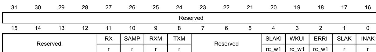
| 31 | 30 | 29 | 28 | 27 | 26 | 25 | 24 | 23 | 22 | 21 | 20 | 19 | 18 | 17 | 16 |
| Reserved | |||||||||||||||
| 15 | 14 | 13 | 12 | 11 | 10 | 9 | 8 | 7 | 6 | 5 | 4 | 3 | 2 | 1 | 0 |
| Reserved. | RX | SAMP | RXM | TXM | Reserved | SLAKI | WKUI | ERRI | SLAK | INAK | |||||
| r | r | r | r | rc_w1 | rc_w1 | rc_w1 | r | r | |||||||
Bits 31:12 Reserved, must be kept at reset value.
Bit 11 RX : CAN Rx signal
Monitors the actual value of the CAN_RX Pin.
Bit 10 SAMP : Last sample point
The value of RX on the last sample point (current received bit value).
Bit 9 RXM : Receive mode
The CAN hardware is currently receiver.
Bit 8 TXM : Transmit mode
The CAN hardware is currently transmitter.
Bits 7:5 Reserved, must be kept at reset value.
Bit 4 SLAKI : Sleep acknowledge interrupt
When SLKIE=1, this bit is set by hardware to signal that the bxCAN has entered Sleep Mode. When set, this bit generates a status change interrupt if the SLKIE bit in the CAN_IER register is set.
This bit is cleared by software or by hardware, when SLAK is cleared.
Note: When SLKIE=0, no polling on SLAKI is possible. In this case the SLAK bit can be polled.
Bit 3 WKUI : Wakeup interrupt
This bit is set by hardware to signal that a SOF bit has been detected while the CAN hardware was in Sleep mode. Setting this bit generates a status change interrupt if the WKUIE bit in the CAN_IER register is set.
This bit is cleared by software.
Bit 2 ERRI : Error interruptThis bit is set by hardware when a bit of the CAN_ESR has been set on error detection and the corresponding interrupt in the CAN_IER is enabled. Setting this bit generates a status change interrupt if the ERRIE bit in the CAN_IER register is set.
This bit is cleared by software.
Bit 1 SLAK : Sleep acknowledgeThis bit is set by hardware and indicates to the software that the CAN hardware is now in Sleep mode. This bit acknowledges the Sleep mode request from the software (set SLEEP bit in CAN_MCR register).
This bit is cleared by hardware when the CAN hardware has left Sleep mode (to be synchronized on the CAN bus). To be synchronized the hardware has to monitor a sequence of 11 consecutive recessive bits on the CAN RX signal.
Note: The process of leaving Sleep mode is triggered when the SLEEP bit in the CAN_MCR register is cleared. Refer to the AWUM bit of the CAN_MCR register description for detailed information for clearing SLEEP bit
Bit 0 INAK : Initialization acknowledgeThis bit is set by hardware and indicates to the software that the CAN hardware is now in initialization mode. This bit acknowledges the initialization request from the software (set INRQ bit in CAN_MCR register).
This bit is cleared by hardware when the CAN hardware has left the initialization mode (to be synchronized on the CAN bus). To be synchronized the hardware has to monitor a sequence of 11 consecutive recessive bits on the CAN RX signal.
CAN transmit status register (CAN_TSR)
Address offset: 0x08
Reset value: 0x1C00 0000
| 31 | 30 | 29 | 28 | 27 | 26 | 25 | 24 | 23 | 22 | 21 | 20 | 19 | 18 | 17 | 16 |
|---|---|---|---|---|---|---|---|---|---|---|---|---|---|---|---|
| LOW2 | LOW1 | LOW0 | TME2 | TME1 | TME0 | CODE[1:0] | ABRQ2 | Reserved | TERR2 | ALST2 | |||||
| r | r | r | r | r | r | r | r | rs | rc_w1 | rc_w1 | |||||
| 15 | 14 | 13 | 12 | 11 | 10 | 9 | 8 | 7 | 6 | 5 | 4 | 3 | 2 | 1 | 0 |
|---|---|---|---|---|---|---|---|---|---|---|---|---|---|---|---|
| ABRQ1 | Reserved | TERR1 | ALST1 | TXOK1 | RQCP1 | ABRQ0 | Reserved | TERR0 | ALST0 | ||||||
| rs | Res. | rc_w1 | rc_w1 | rc_w1 | rc_w1 | rs | rc_w1 | rc_w1 | |||||||
This bit is set by hardware when more than one mailbox are pending for transmission and mailbox 2 has the lowest priority.
Bit 30 LOW1 : Lowest priority flag for mailbox 1This bit is set by hardware when more than one mailbox are pending for transmission and mailbox 1 has the lowest priority.
Bit 29 LOW0 : Lowest priority flag for mailbox 0This bit is set by hardware when more than one mailbox are pending for transmission and mailbox 0 has the lowest priority.
Note: The LOW[2:0] bits are set to zero when only one mailbox is pending.
Bit 28 TME2 : Transmit mailbox 2 emptyThis bit is set by hardware when no transmit request is pending for mailbox 2.
Bit 27 TME1 : Transmit mailbox 1 emptyThis bit is set by hardware when no transmit request is pending for mailbox 1.
Bit 26 TME0 : Transmit mailbox 0 empty
This bit is set by hardware when no transmit request is pending for mailbox 0.
Bits 25:24 CODE[1:0] : Mailbox code
In case at least one transmit mailbox is free, the code value is equal to the number of the next transmit mailbox free.
In case all transmit mailboxes are pending, the code value is equal to the number of the transmit mailbox with the lowest priority.
Bit 23 ABRQ2 : Abort request for mailbox 2
Set by software to abort the transmission request for the corresponding mailbox.
Cleared by hardware when the mailbox becomes empty.
Setting this bit has no effect when the mailbox is not pending for transmission.
Bits 22:20 Reserved, must be kept at reset value.
Bit 19 TERR2 : Transmission error of mailbox 2
This bit is set when the previous TX failed due to an error.
Bit 18 ALST2 : Arbitration lost for mailbox 2
This bit is set when the previous TX failed due to an arbitration lost.
Bit 17 TXOK2 : Transmission OK of mailbox 2
The hardware updates this bit after each transmission attempt.
0: The previous transmission failed
1: The previous transmission was successful
This bit is set by hardware when the transmission request on mailbox 2 has been completed successfully. Refer to Figure 228 .
Bit 16 RQCP2 : Request completed mailbox 2
Set by hardware when the last request (transmit or abort) has been performed.
Cleared by software writing a “1” or by hardware on transmission request (TXRQ2 set in CAN_TMID2R register).
Clearing this bit clears all the status bits (TXOK2, ALST2 and TERR2) for Mailbox 2.
Bit 15 ABRQ1 : Abort request for mailbox 1
Set by software to abort the transmission request for the corresponding mailbox.
Cleared by hardware when the mailbox becomes empty.
Setting this bit has no effect when the mailbox is not pending for transmission.
Bits 14:12 Reserved, must be kept at reset value.
Bit 11 TERR1 : Transmission error of mailbox 1
This bit is set when the previous TX failed due to an error.
Bit 10 ALST1 : Arbitration lost for mailbox 1
This bit is set when the previous TX failed due to an arbitration lost.
Bit 9 TXOK1 : Transmission OK of mailbox 1
The hardware updates this bit after each transmission attempt.
0: The previous transmission failed
1: The previous transmission was successful
This bit is set by hardware when the transmission request on mailbox 1 has been completed successfully. Refer to Figure 228 .
Bit 8 RQCP1 : Request completed mailbox 1
Set by hardware when the last request (transmit or abort) has been performed.
Cleared by software writing a “1” or by hardware on transmission request (TXRQ1 set in CAN_TI1R register).
Clearing this bit clears all the status bits (TXOK1, ALST1 and TERR1) for Mailbox 1.
Bit 7 ABRQ0 : Abort request for mailbox0
Set by software to abort the transmission request for the corresponding mailbox.
Cleared by hardware when the mailbox becomes empty.
Setting this bit has no effect when the mailbox is not pending for transmission.
Bits 6:4 Reserved, must be kept at reset value.
Bit 3 TERR0 : Transmission error of mailbox0
This bit is set when the previous TX failed due to an error.
Bit 2 ALST0 : Arbitration lost for mailbox0
This bit is set when the previous TX failed due to an arbitration lost.
Bit 1 TXOK0 : Transmission OK of mailbox0
The hardware updates this bit after each transmission attempt.
0: The previous transmission failed
1: The previous transmission was successful
This bit is set by hardware when the transmission request on mailbox 1 has been completed successfully. Refer to Figure 228
Bit 0 RQCP0 : Request completed mailbox0
Set by hardware when the last request (transmit or abort) has been performed.
Cleared by software writing a “1” or by hardware on transmission request (TXRQ0 set in CAN_TIR register).
Clearing this bit clears all the status bits (TXOK0, ALST0 and TERR0) for Mailbox 0.
CAN receive FIFO 0 register (CAN_RF0R)
Address offset: 0x0C
Reset value: 0x0000 0000
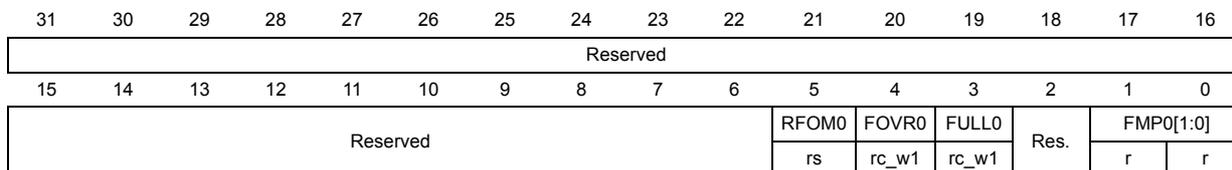
| 31 | 30 | 29 | 28 | 27 | 26 | 25 | 24 | 23 | 22 | 21 | 20 | 19 | 18 | 17 | 16 |
| Reserved | |||||||||||||||
| 15 | 14 | 13 | 12 | 11 | 10 | 9 | 8 | 7 | 6 | 5 | 4 | 3 | 2 | 1 | 0 |
| Reserved | RFOM0 | FOVR0 | FULL0 | Res. | FMP0[1:0] | ||||||||||
| rs | rc_w1 | rc_w1 | r | r | |||||||||||
Bits 31:6 Reserved, must be kept at reset value.
Bit 5 RFOM0 : Release FIFO 0 output mailbox
Set by software to release the output mailbox of the FIFO. The output mailbox can only be released when at least one message is pending in the FIFO. Setting this bit when the FIFO is empty has no effect. If at least two messages are pending in the FIFO, the software has to release the output mailbox to access the next message.
Cleared by hardware when the output mailbox has been released.
Bit 4 FOVR0 : FIFO 0 overrun
This bit is set by hardware when a new message has been received and passed the filter while the FIFO was full.
This bit is cleared by software.
Bit 3 FULL0 : FIFO 0 full
Set by hardware when three messages are stored in the FIFO.
This bit is cleared by software.
Bit 2 Reserved, must be kept at reset value.
Bits 1:0 FMP0[1:0] : FIFO 0 message pending
These bits indicate how many messages are pending in the receive FIFO.
FMP is increased each time the hardware stores a new message in to the FIFO. FMP is decreased each time the software releases the output mailbox by setting the RFOM0 bit.
CAN receive FIFO 1 register (CAN_RF1R)
Address offset: 0x10
Reset value: 0x0000 0000
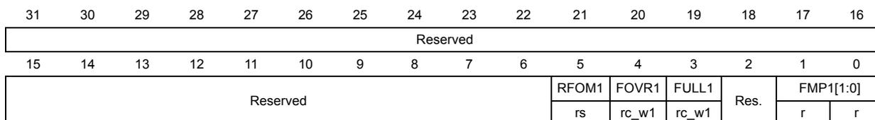
| 31 | 30 | 29 | 28 | 27 | 26 | 25 | 24 | 23 | 22 | 21 | 20 | 19 | 18 | 17 | 16 |
| Reserved | |||||||||||||||
| 15 | 14 | 13 | 12 | 11 | 10 | 9 | 8 | 7 | 6 | 5 | 4 | 3 | 2 | 1 | 0 |
| Reserved | RFOM1 | FOVR1 | FULL1 | Res. | FMP1[1:0] | ||||||||||
| rs | rc_w1 | rc_w1 | r | r | |||||||||||
Bits 31:6 Reserved, must be kept at reset value.
Bit 5 RFOM1 : Release FIFO 1 output mailbox
Set by software to release the output mailbox of the FIFO. The output mailbox can only be released when at least one message is pending in the FIFO. Setting this bit when the FIFO is empty has no effect. If at least two messages are pending in the FIFO, the software has to release the output mailbox to access the next message.
Cleared by hardware when the output mailbox has been released.
Bit 4 FOVR1 : FIFO 1 overrun
This bit is set by hardware when a new message has been received and passed the filter while the FIFO was full.
This bit is cleared by software.
Bit 3 FULL1 : FIFO 1 full
Set by hardware when three messages are stored in the FIFO.
This bit is cleared by software.
Bit 2 Reserved, must be kept at reset value.
Bits 1:0 FMP1[1:0] : FIFO 1 message pending
These bits indicate how many messages are pending in the receive FIFO1.
FMP1 is increased each time the hardware stores a new message in to the FIFO1. FMP is decreased each time the software releases the output mailbox by setting the RFOM1 bit.
CAN interrupt enable register (CAN_IER)
Address offset: 0x14
Reset value: 0x0000 0000
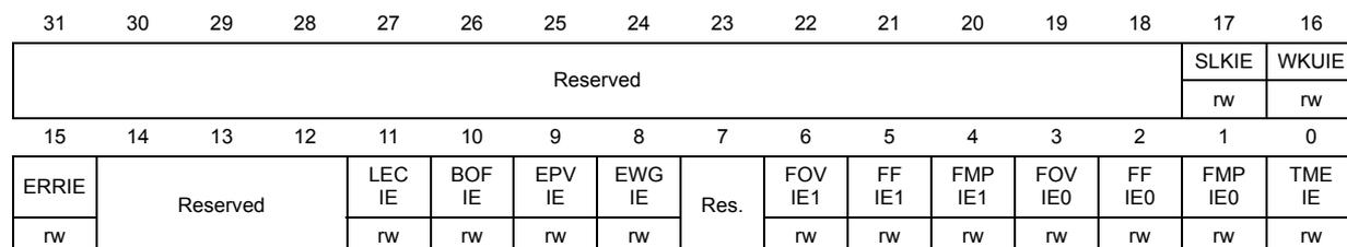
| 31 | 30 | 29 | 28 | 27 | 26 | 25 | 24 | 23 | 22 | 21 | 20 | 19 | 18 | 17 | 16 |
| Reserved | SLKIE | WKUIE | |||||||||||||
| rw | rw | ||||||||||||||
| 15 | 14 | 13 | 12 | 11 | 10 | 9 | 8 | 7 | 6 | 5 | 4 | 3 | 2 | 1 | 0 |
| ERRIE | Reserved | LEC IE | BOF IE | EPV IE | EWG IE | Res. | FOV IE1 | FF IE1 | FMP IE1 | FOV IE0 | FF IE0 | FMP IE0 | TME IE | ||
| rw | rw | rw | rw | rw | rw | rw | rw | rw | rw | rw | rw | ||||
Bits 31:18 Reserved, must be kept at reset value.
Bit 17 SLKIE : Sleep interrupt enable
0: No interrupt when SLAKI bit is set.
1: Interrupt generated when SLAKI bit is set.
Bit 16 WKUIE : Wakeup interrupt enable
0: No interrupt when WKUI is set.
1: Interrupt generated when WKUI bit is set.
Bit 15 ERRIE : Error interrupt enable
0: No interrupt will be generated when an error condition is pending in the CAN_ESR.
1: An interrupt will be generated when an error condition is pending in the CAN_ESR.
Bits 14:12 Reserved, must be kept at reset value.
Bit 11 LECIE : Last error code interrupt enable
0: ERRI bit will not be set when the error code in LEC[2:0] is set by hardware on error detection.
1: ERRI bit will be set when the error code in LEC[2:0] is set by hardware on error detection.
Bit 10 BOFIE : Bus-off interrupt enable
0: ERRI bit will not be set when BOFF is set.
1: ERRI bit will be set when BOFF is set.
Bit 9 EPVIE : Error passive interrupt enable
0: ERRI bit will not be set when EPVF is set.
1: ERRI bit will be set when EPVF is set.
Bit 8 EWGIE : Error warning interrupt enable
0: ERRI bit will not be set when EWGF is set.
1: ERRI bit will be set when EWGF is set.
Bit 7 Reserved, must be kept at reset value.
Bit 6 FOVIE1 : FIFO overrun interrupt enable
0: No interrupt when FOVR is set.
1: Interrupt generation when FOVR is set.
Bit 5 FFIE1 : FIFO full interrupt enable
0: No interrupt when FULL bit is set.
1: Interrupt generated when FULL bit is set.
Bit 4 FMPIE1 : FIFO message pending interrupt enable
0: No interrupt generated when state of FMP[1:0] bits are not 00b.
1: Interrupt generated when state of FMP[1:0] bits are not 00b.
Bit 3 FOVIE0 : FIFO overrun interrupt enable
0: No interrupt when FOVR bit is set.
1: Interrupt generated when FOVR bit is set.
Bit 2 FFIE0 : FIFO full interrupt enable
0: No interrupt when FULL bit is set.
1: Interrupt generated when FULL bit is set.
Bit 1 FMPIE0 : FIFO message pending interrupt enable
0: No interrupt generated when state of FMP[1:0] bits are not 00b.
1: Interrupt generated when state of FMP[1:0] bits are not 00b.
Bit 0 TMEIE : Transmit mailbox empty interrupt enable
0: No interrupt when RQCPx bit is set.
1: Interrupt generated when RQCPx bit is set.
Note: Refer to Section 24.8: bxCAN interrupts.
CAN error status register (CAN_ESR)
Address offset: 0x18
Reset value: 0x0000 0000
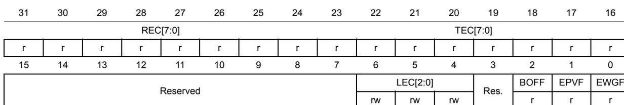
| 31 | 30 | 29 | 28 | 27 | 26 | 25 | 24 | 23 | 22 | 21 | 20 | 19 | 18 | 17 | 16 |
| REC[7:0] | TEC[7:0] | ||||||||||||||
| r | r | r | r | r | r | r | r | r | r | r | r | r | r | r | r |
| 15 | 14 | 13 | 12 | 11 | 10 | 9 | 8 | 7 | 6 | 5 | 4 | 3 | 2 | 1 | 0 |
| Reserved | LEC[2:0] | Res. | BOFF | EPVF | EWGF | ||||||||||
| rw | rw | rw | r | r | r | ||||||||||
Bits 31:24 REC[7:0] : Receive error counter
The implementing part of the fault confinement mechanism of the CAN protocol. In case of an error during reception, this counter is incremented by 1 or by 8 depending on the error condition as defined by the CAN standard. After every successful reception the counter is decremented by 1 or reset to 120 if its value was higher than 128. When the counter value exceeds 127, the CAN controller enters the error passive state.
Bits 23:16 TEC[7:0] : Least significant byte of the 9-bit transmit error counter
The implementing part of the fault confinement mechanism of the CAN protocol.
Bits 15:7 Reserved, must be kept at reset value.
Bits 6:4 LEC[2:0] : Last error code
This field is set by hardware and holds a code which indicates the error condition of the last error detected on the CAN bus. If a message has been transferred (reception or transmission) without error, this field will be cleared to '0'.
The LEC[2:0] bits can be set to value 0b111 by software. They are updated by hardware to indicate the current communication status.
000: No Error
001: Stuff Error
010: Form Error
011: Acknowledgment Error
100: Bit recessive Error
101: Bit dominant Error
110: CRC Error
111: Set by software
Bit 3 Reserved, must be kept at reset value.
Bit 2 BOFF : Bus-off flag
This bit is set by hardware when it enters the bus-off state. The bus-off state is entered on TEC overflow, greater than 255, refer to Section 24.7.6 .
Bit 1 EPVF : Error passive flag
This bit is set by hardware when the Error Passive limit has been reached (Receive Error Counter or Transmit Error Counter > 127).
Bit 0 EWGF : Error warning flag
This bit is set by hardware when the warning limit has been reached (Receive Error Counter or Transmit Error Counter ≥ 96).
CAN bit timing register (CAN_BTR)
Address offset: 0x1C
Reset value: 0x0123 0000
This register can only be accessed by the software when the CAN hardware is in initialization mode.
| 31 | 30 | 29 | 28 | 27 | 26 | 25 | 24 | 23 | 22 | 21 | 20 | 19 | 18 | 17 | 16 |
|---|---|---|---|---|---|---|---|---|---|---|---|---|---|---|---|
| SILM | LBKM | Reserved | SJW[1:0] | Res. | TS2[2:0] | TS1[3:0] | |||||||||
| rw | rw | rw | rw | rw | rw | rw | rw | rw | rw | rw | |||||
| 15 | 14 | 13 | 12 | 11 | 10 | 9 | 8 | 7 | 6 | 5 | 4 | 3 | 2 | 1 | 0 |
|---|---|---|---|---|---|---|---|---|---|---|---|---|---|---|---|
| Reserved | BRP[9:0] | ||||||||||||||
| rw | rw | rw | rw | rw | rw | rw | rw | rw | rw | ||||||
Bit 31 SILM : Silent mode (debug)
0: Normal operation
1: Silent Mode
Bit 30 LBKM : Loop back mode (debug)
0: Loop Back Mode disabled
1: Loop Back Mode enabled
Bits 29:26 Reserved, must be kept at reset value.
Bits 25:24 SJW[1:0] : Resynchronization jump width
These bits define the maximum number of time quanta the CAN hardware is allowed to lengthen or shorten a bit to perform the resynchronization.
Bit 23 Reserved, must be kept at reset value.
Bits 22:20 TS2[2:0] : Time segment 2
These bits define the number of time quanta in Time Segment 2.
Bits 19:16 TS1[3:0] : Time segment 1
These bits define the number of time quanta in Time Segment 1
\( t_{BS1} = t_q \times (TS1[3:0] + 1) \)
For more information on bit timing refer to Section 24.7.7 .
Bits 15:10 Reserved, must be kept at reset value.
Bits 9:0 BRP[9:0] : Baud rate prescaler
These bits define the length of a time quanta.
\( t_q = (BRP[9:0] + 1) \times t_{PCLK} \)
24.9.3 CAN mailbox registers
This chapter describes the registers of the transmit and receive mailboxes. Refer to Section 24.7.5: Message storage for detailed register mapping.
Transmit and receive mailboxes have the same registers except:
- • The FMI field in the CAN_RDTxR register.
- • A receive mailbox is always write protected.
- • A transmit mailbox is write-enabled only while empty, corresponding TME bit in the CAN_TSR register set.
There are three TX Mailboxes and two RX Mailboxes , as shown in Figure 237 . Each RX Mailbox allows access to a 3-level depth FIFO, the access being offered only to the oldest received message in the FIFO. Each mailbox consist of four registers.
Figure 237. RX and TX mailboxes
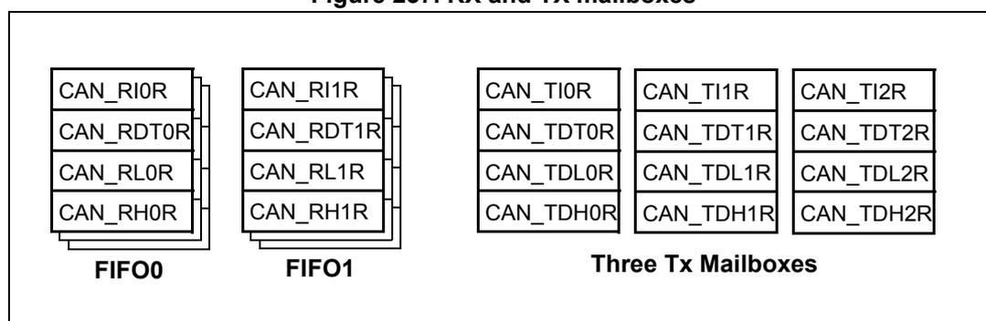
The diagram illustrates the structure of the CAN mailboxes. It is divided into three main sections: FIFO0, FIFO1, and Three Tx Mailboxes.
- FIFO0 and FIFO1 are receive mailboxes. Each consists of four stacked registers. For FIFO0: CAN_RI0R, CAN_RDT0R, CAN_RL0R, and CAN_RH0R. For FIFO1: CAN_RI1R, CAN_RDT1R, CAN_RL1R, and CAN_RH1R. The labels FIFO0 and FIFO1 are placed below the respective stacks of registers.
- Three Tx Mailboxes
are transmit mailboxes. There are three columns, each with four stacked registers.
- Mailbox 0: CAN_TI0R, CAN_TDT0R, CAN_TDL0R, CAN_TDH0R
- Mailbox 1: CAN_TI1R, CAN_TDT1R, CAN_TDL1R, CAN_TDH1R
- Mailbox 2: CAN_TI2R, CAN_TDT2R, CAN_TDL2R, CAN_TDH2R
Address offsets: 0x180, 0x190, 0x1A0
Reset value: 0xXXXX XXXX (except bit 0, TXRQ = 0)
All TX registers are write protected when the mailbox is pending transmission (TMEx reset).
This register also implements the TX request control (bit 0) - reset value 0.
| 31 | 30 | 29 | 28 | 27 | 26 | 25 | 24 | 23 | 22 | 21 | 20 | 19 | 18 | 17 | 16 |
|---|---|---|---|---|---|---|---|---|---|---|---|---|---|---|---|
| STID[10:0]/EXID[28:18] | EXID[17:13] | ||||||||||||||
| rw | rw | rw | rw | rw | rw | rw | rw | rw | rw | rw | rw | rw | rw | rw | rw |
| 15 | 14 | 13 | 12 | 11 | 10 | 9 | 8 | 7 | 6 | 5 | 4 | 3 | 2 | 1 | 0 |
| EXID[12:0] | IDE | RTR | TXRQ | ||||||||||||
| rw | rw | rw | rw | rw | rw | rw | rw | rw | rw | rw | rw | rw | rw | rw | rw |
The standard identifier or the MSBs of the extended identifier (depending on the IDE bit value).
Bits 20:3 EXID[17:0] : Extended identifierThe LSBs of the extended identifier.
Bit 2 IDE : Identifier extensionThis bit defines the identifier type of message in the mailbox.
0: Standard identifier.
1: Extended identifier.
Bit 1 RTR : Remote transmission request0: Data frame
1: Remote frame
Bit 0 TXRQ : Transmit mailbox requestSet by software to request the transmission for the corresponding mailbox.
Cleared by hardware when the mailbox becomes empty.
CAN mailbox data length control and time stamp register (CAN_TDTxR) (x=0..2)
All bits of this register are write protected when the mailbox is not in empty state.
Address offsets: 0x184, 0x194, 0x1A4
Reset value: 0xXXXX XXXX
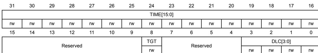
| 31 | 30 | 29 | 28 | 27 | 26 | 25 | 24 | 23 | 22 | 21 | 20 | 19 | 18 | 17 | 16 |
| TIME[15:0] | |||||||||||||||
| rw | rw | rw | rw | rw | rw | rw | rw | rw | rw | rw | rw | rw | rw | rw | rw |
| 15 | 14 | 13 | 12 | 11 | 10 | 9 | 8 | 7 | 6 | 5 | 4 | 3 | 2 | 1 | 0 |
| Reserved | TGT | Reserved | DLC[3:0] | ||||||||||||
| rw | rw | rw | rw | rw | |||||||||||
Bits 31:16 TIME[15:0] : Message time stamp
This field contains the 16-bit timer value captured at the SOF transmission.
Bits 15:9 Reserved, must be kept at reset value.
Bit 8 TGT : Transmit global time
This bit is active only when the hardware is in the Time Trigger Communication mode, TTCM bit of the CAN_MCR register is set.
0: Time stamp TIME[15:0] is not sent.
1: Time stamp TIME[15:0] value is sent in the last two data bytes of the 8-byte message:
TIME[7:0] in data byte 7 and TIME[15:8] in data byte 6, replacing the data written in CAN_TDHxR[31:16] register (DATA6[7:0] and DATA7[7:0]). DLC must be programmed as 8 in order these two bytes to be sent over the CAN bus.
Bits 7:4 Reserved, must be kept at reset value.
Bits 3:0 DLC[3:0] : Data length code
This field defines the number of data bytes a data frame contains or a remote frame request.
A message can contain from 0 to 8 data bytes, depending on the value in the DLC field.
CAN mailbox data low register (CAN_TDLxR) (x=0..2)
All bits of this register are write protected when the mailbox is not in empty state.
Address offsets: 0x188, 0x198, 0x1A8
Reset value: 0xXXXX XXXX
| 31 | 30 | 29 | 28 | 27 | 26 | 25 | 24 | 23 | 22 | 21 | 20 | 19 | 18 | 17 | 16 |
|---|---|---|---|---|---|---|---|---|---|---|---|---|---|---|---|
| DATA3[7:0] | DATA2[7:0] | ||||||||||||||
| rw | rw | rw | rw | rw | rw | rw | rw | rw | rw | rw | rw | rw | rw | rw | rw |
| 15 | 14 | 13 | 12 | 11 | 10 | 9 | 8 | 7 | 6 | 5 | 4 | 3 | 2 | 1 | 0 |
| DATA1[7:0] | DATA0[7:0] | ||||||||||||||
| rw | rw | rw | rw | rw | rw | rw | rw | rw | rw | rw | rw | rw | rw | rw | rw |
Bits 31:24 DATA3[7:0] : Data byte 3
Data byte 3 of the message.
Bits 23:16 DATA2[7:0] : Data byte 2
Data byte 2 of the message.
Bits 15:8 DATA1[7:0] : Data byte 1
Data byte 1 of the message.
Bits 7:0 DATA0[7:0] : Data byte 0
Data byte 0 of the message.
A message can contain from 0 to 8 data bytes and starts with byte 0.
CAN mailbox data high register (CAN_TDHxR) (x=0..2)
All bits of this register are write protected when the mailbox is not in empty state.
Address offsets: 0x18C, 0x19C, 0x1AC
Reset value: 0xXXXX XXXX
| 31 | 30 | 29 | 28 | 27 | 26 | 25 | 24 | 23 | 22 | 21 | 20 | 19 | 18 | 17 | 16 |
|---|---|---|---|---|---|---|---|---|---|---|---|---|---|---|---|
| DATA7[7:0] | DATA6[7:0] | ||||||||||||||
| rw | rw | rw | rw | rw | rw | rw | rw | rw | rw | rw | rw | rw | rw | rw | rw |
| 15 | 14 | 13 | 12 | 11 | 10 | 9 | 8 | 7 | 6 | 5 | 4 | 3 | 2 | 1 | 0 |
| DATA5[7:0] | DATA4[7:0] | ||||||||||||||
| rw | rw | rw | rw | rw | rw | rw | rw | rw | rw | rw | rw | rw | rw | rw | rw |
Bits 31:24 DATA7[7:0] : Data byte 7
Data byte 7 of the message.
Note: If TGT of this message and TTCM are active, DATA7 and DATA6 will be replaced by the TIME stamp value.
Bits 23:16 DATA6[7:0] : Data byte 6
Data byte 6 of the message.
Bits 15:8 DATA5[7:0] : Data byte 5
Data byte 5 of the message.
Bits 7:0 DATA4[7:0] : Data byte 4
Data byte 4 of the message.
CAN receive FIFO mailbox identifier register (CAN_RIxR) (x=0..1)
Address offsets: 0x1B0, 0x1C0
Reset value: 0xXXXX XXXX
All RX registers are write protected.
| 31 | 30 | 29 | 28 | 27 | 26 | 25 | 24 | 23 | 22 | 21 | 20 | 19 | 18 | 17 | 16 |
|---|---|---|---|---|---|---|---|---|---|---|---|---|---|---|---|
| STID[10:0]/EXID[28:18] | EXID[17:13] | ||||||||||||||
| r | r | r | r | r | r | r | r | r | r | r | r | r | r | r | r |
| 15 | 14 | 13 | 12 | 11 | 10 | 9 | 8 | 7 | 6 | 5 | 4 | 3 | 2 | 1 | 0 |
| EXID[12:0] | IDE | RTR | Res. | ||||||||||||
| r | r | r | r | r | r | r | r | r | r | r | r | r | r | r | |
Bits 31:21 STID[10:0]/EXID[28:18] : Standard identifier or extended identifier
The standard identifier or the MSBs of the extended identifier (depending on the IDE bit value).
Bits 20:3 EXID[17:0] : Extended identifier
The LSBs of the extended identifier.
Bit 2 IDE : Identifier extension
This bit defines the identifier type of message in the mailbox.
0: Standard identifier.
1: Extended identifier.
Bit 1 RTR : Remote transmission request
0: Data frame
1: Remote frame
Bit 0 Reserved, must be kept at reset value.
CAN receive FIFO mailbox data length control and time stamp register
(CAN_RDTxR) (x=0..1)
Address offsets: 0x1B4, 0x1C4
Reset value: 0xXXXX XXXX
All RX registers are write protected.
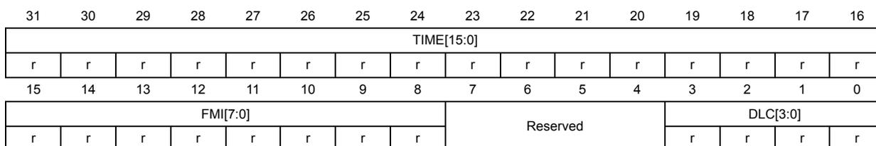
| 31 | 30 | 29 | 28 | 27 | 26 | 25 | 24 | 23 | 22 | 21 | 20 | 19 | 18 | 17 | 16 |
| TIME[15:0] | |||||||||||||||
| r | r | r | r | r | r | r | r | r | r | r | r | r | r | r | r |
| 15 | 14 | 13 | 12 | 11 | 10 | 9 | 8 | 7 | 6 | 5 | 4 | 3 | 2 | 1 | 0 |
| FMI[7:0] | Reserved | DLC[3:0] | |||||||||||||
| r | r | r | r | r | r | r | r | r | r | r | r | ||||
Bits 31:16 TIME[15:0] : Message time stamp
This field contains the 16-bit timer value captured at the SOF detection.
Bits 15:8 FMI[7:0] : Filter match index
This register contains the index of the filter the message stored in the mailbox passed through. For more details on identifier filtering refer to Section 24.7.4
Bits 7:4 Reserved, must be kept at reset value.
Bits 3:0 DLC[3:0] : Data length code
This field defines the number of data bytes a data frame contains (0 to 8). It is 0 in the case of a remote frame request.
CAN receive FIFO mailbox data low register (CAN_RDLxR) (x=0..1)All bits of this register are write protected when the mailbox is not in empty state.
Address offsets: 0x1B8, 0x1C8
Reset value: 0xXXXX XXXX
All RX registers are write protected.
| 31 | 30 | 29 | 28 | 27 | 26 | 25 | 24 | 23 | 22 | 21 | 20 | 19 | 18 | 17 | 16 |
| DATA3[7:0] | DATA2[7:0] | ||||||||||||||
| r | r | r | r | r | r | r | r | r | r | r | r | r | r | r | r |
| 15 | 14 | 13 | 12 | 11 | 10 | 9 | 8 | 7 | 6 | 5 | 4 | 3 | 2 | 1 | 0 |
| DATA1[7:0] | DATA0[7:0] | ||||||||||||||
| r | r | r | r | r | r | r | r | r | r | r | r | r | r | r | r |
Bits 31:24 DATA3[7:0] : Data Byte 3
Data byte 3 of the message.
Bits 23:16 DATA2[7:0] : Data Byte 2
Data byte 2 of the message.
Bits 15:8 DATA1[7:0] : Data Byte 1
Data byte 1 of the message.
Bits 7:0 DATA0[7:0] : Data Byte 0
Data byte 0 of the message.
A message can contain from 0 to 8 data bytes and starts with byte 0.
CAN receive FIFO mailbox data high register (CAN_RDHxR) (x=0..1)Address offsets: 0x1BC, 0x1CC
Reset value: 0xXXXX XXXX
All RX registers are write protected.
| 31 | 30 | 29 | 28 | 27 | 26 | 25 | 24 | 23 | 22 | 21 | 20 | 19 | 18 | 17 | 16 |
| DATA7[7:0] | DATA6[7:0] | ||||||||||||||
| r | r | r | r | r | r | r | r | r | r | r | r | r | r | r | r |
| 15 | 14 | 13 | 12 | 11 | 10 | 9 | 8 | 7 | 6 | 5 | 4 | 3 | 2 | 1 | 0 |
| DATA5[7:0] | DATA4[7:0] | ||||||||||||||
| r | r | r | r | r | r | r | r | r | r | r | r | r | r | r | r |
Bits 31:24 DATA7[7:0] : Data Byte 7
Data byte 3 of the message.
Bits 23:16 DATA6[7:0] : Data Byte 6
Data byte 2 of the message.
Bits 15:8 DATA5[7:0] : Data Byte 5
Data byte 1 of the message.
Bits 7:0 DATA4[7:0] : Data Byte 4
Data byte 0 of the message.
24.9.4 CAN filter registers
CAN filter master register (CAN_FMR)
Address offset: 0x200
Reset value: 0x2A1C 0E01
All bits of this register are set and cleared by software.
| 31 | 30 | 29 | 28 | 27 | 26 | 25 | 24 | 23 | 22 | 21 | 20 | 19 | 18 | 17 | 16 |
| Reserved | |||||||||||||||
| 15 | 14 | 13 | 12 | 11 | 10 | 9 | 8 | 7 | 6 | 5 | 4 | 3 | 2 | 1 | 0 |
| Reserved | CAN2SB[5:0] | Reserved | FINIT | ||||||||||||
| rw | rw | rw | rw | rw | rw | rw | |||||||||
Bits 31:14 Reserved, must be kept at reset value.
Bits 13:8 CAN2SB[5:0] : CAN2 start bank
These bits are set and cleared by software. They define the start bank for the CAN2 interface (Slave) in the range 0 to 27.
Note: When CAN2SB[5:0] = 28d, all the filters to CAN1 can be used.
When CAN2SB[5:0] is set to 0, no filters are assigned to CAN1.
Bits 7:1 Reserved, must be kept at reset value.
Bit 0 FINIT : Filter init mode
Initialization mode for filter banks
0: Active filters mode.
1: Initialization mode for the filters.
CAN filter mode register (CAN_FM1R)Address offset: 0x204
Reset value: 0x0000 0000
This register can be written only when the filter initialization mode is set (FINIT=1) in the CAN_FMR register.
| 31 | 30 | 29 | 28 | 27 | 26 | 25 | 24 | 23 | 22 | 21 | 20 | 19 | 18 | 17 | 16 |
|---|---|---|---|---|---|---|---|---|---|---|---|---|---|---|---|
| Reserved | FBM27 | FBM26 | FBM25 | FBM24 | FBM23 | FBM22 | FBM21 | FBM20 | FBM19 | FBM18 | FBM17 | ||||
| rw | rw | rw | rw | rw | rw | rw | rw | rw | rw | rw | |||||
| 15 | 14 | 13 | 12 | 11 | 10 | 9 | 8 | 7 | 6 | 5 | 4 | 3 | 2 | 1 | 0 |
| FBM15 | FBM14 | FBM13 | FBM12 | FBM11 | FBM10 | FBM9 | FBM8 | FBM7 | FBM6 | FBM5 | FBM4 | FBM3 | FBM2 | FBM1 | FBM0 |
| rw | rw | rw | rw | rw | rw | rw | rw | rw | rw | rw | rw | rw | rw | rw | rw |
Note: Refer to Figure 230.
Bits 31:28 Reserved, must be kept at reset value.
Bits 27:0 FBMx : Filter mode
Mode of the registers of Filter x.
0: Two 32-bit registers of filter bank x are in Identifier Mask mode.
1: Two 32-bit registers of filter bank x are in Identifier List mode.
Note: Bits 27:14 are available in connectivity line devices only and are reserved otherwise.
CAN filter scale register (CAN_FS1R)Address offset: 0x20C
Reset value: 0x0000 0000
This register can be written only when the filter initialization mode is set (FINIT=1) in the CAN_FMR register.
| 31 | 30 | 29 | 28 | 27 | 26 | 25 | 24 | 23 | 22 | 21 | 20 | 19 | 18 | 17 | 16 |
|---|---|---|---|---|---|---|---|---|---|---|---|---|---|---|---|
| Reserved | FSC27 | FSC26 | FSC25 | FSC24 | FSC23 | FSC22 | FSC21 | FSC20 | FSC19 | FSC18 | FSC17 | ||||
| rw | rw | rw | rw | rw | rw | rw | rw | rw | rw | rw | |||||
| 15 | 14 | 13 | 12 | 11 | 10 | 9 | 8 | 7 | 6 | 5 | 4 | 3 | 2 | 1 | 0 |
| FSC15 | FSC14 | FSC13 | FSC12 | FSC11 | FSC10 | FSC9 | FSC8 | FSC7 | FSC6 | FSC5 | FSC4 | FSC3 | FSC2 | FSC1 | FSC0 |
| rw | rw | rw | rw | rw | rw | rw | rw | rw | rw | rw | rw | rw | rw | rw | rw |
Bits 31:28 Reserved, must be kept at reset value.
Bits 27:0 FSCx : Filter scale configuration
These bits define the scale configuration of Filters 13-0.
0: Dual 16-bit scale configuration
1: Single 32-bit scale configuration
Note: Bits 27:14 are available in connectivity line devices only and are reserved otherwise.
Note: Refer to Figure 230.
CAN filter FIFO assignment register (CAN_FFA1R)
Address offset: 0x214
Reset value: 0x0000 0000
This register can be written only when the filter initialization mode is set (FINIT=1) in the CAN_FMR register.
| 31 | 30 | 29 | 28 | 27 | 26 | 25 | 24 | 23 | 22 | 21 | 20 | 19 | 18 | 17 | 16 |
|---|---|---|---|---|---|---|---|---|---|---|---|---|---|---|---|
| Reserved | FFA27 | FFA26 | FFA25 | FFA24 | FFA23 | FFA22 | FFA21 | FFA20 | FFA19 | FFA18 | FFA17 | FFA16 | |||
| rw | rw | rw | rw | rw | rw | rw | rw | rw | rw | rw | rw | ||||
| 15 | 14 | 13 | 12 | 11 | 10 | 9 | 8 | 7 | 6 | 5 | 4 | 3 | 2 | 1 | 0 |
| FFA15 | FFA14 | FFA13 | FFA12 | FFA11 | FFA10 | FFA9 | FFA8 | FFA7 | FFA6 | FFA5 | FFA4 | FFA3 | FFA2 | FFA1 | FFA0 |
| rw | rw | rw | rw | rw | rw | rw | rw | rw | rw | rw | rw | rw | rw | rw | rw |
Bits 31:28 Reserved, must be kept at reset value.
Bits 27:0 FFAx : Filter FIFO assignment for filter x
The message passing through this filter will be stored in the specified FIFO.
0: Filter assigned to FIFO 0
1: Filter assigned to FIFO 1
Note: Bits 27:14 are available in connectivity line devices only and are reserved otherwise.
CAN filter activation register (CAN_FA1R)
Address offset: 0x21C
Reset value: 0x0000 0000
| 31 | 30 | 29 | 28 | 27 | 26 | 25 | 24 | 23 | 22 | 21 | 20 | 19 | 18 | 17 | 16 |
|---|---|---|---|---|---|---|---|---|---|---|---|---|---|---|---|
| Reserved | FACT27 | FACT26 | FACT25 | FACT24 | FACT23 | FACT22 | FACT21 | FACT20 | FACT19 | FACT18 | FACT17 | FACT16 | |||
| rw | rw | rw | rw | rw | rw | rw | rw | rw | rw | rw | rw | ||||
| 15 | 14 | 13 | 12 | 11 | 10 | 9 | 8 | 7 | 6 | 5 | 4 | 3 | 2 | 1 | 0 |
| FACT15 | FACT14 | FACT13 | FACT12 | FACT11 | FACT10 | FACT9 | FACT8 | FACT7 | FACT6 | FACT5 | FACT4 | FACT3 | FACT2 | FACT1 | FACT0 |
| rw | rw | rw | rw | rw | rw | rw | rw | rw | rw | rw | rw | rw | rw | rw | rw |
Bits 31:28 Reserved, must be kept at reset value.
Bits 27:0 FACTx : Filter active
The software sets this bit to activate Filter x. To modify the Filter x registers (CAN_FxR[0:7]), the FACTx bit must be cleared or the FINIT bit of the CAN_FMR register must be set.
0: Filter x is not active
1: Filter x is active
Note: Bits 27:14 are available in connectivity line devices only and are reserved otherwise.
Filter bank i register x (CAN_FiRx) (i=0..27, x=1, 2)
Address offsets: 0x240..0x31C
Reset value: 0xXXXX XXXX
n connectivity line devices there are 28 filter banks, i=0 .. 27, in other devices there are 14 filter banks i = 0 ..13. Each filter bank i is composed of two 32-bit registers, CAN_FiR[2:1].
This register can only be modified when the FACTx bit of the CAN_FAxR register is cleared or when the FINIT bit of the CAN_FMR register is set.
| 31 | 30 | 29 | 28 | 27 | 26 | 25 | 24 | 23 | 22 | 21 | 20 | 19 | 18 | 17 | 16 |
| FB31 | FB30 | FB29 | FB28 | FB27 | FB26 | FB25 | FB24 | FB23 | FB22 | FB21 | FB20 | FB19 | FB18 | FB17 | FB16 |
| rw | rw | rw | rw | rw | rw | rw | rw | rw | rw | rw | rw | rw | rw | rw | rw |
| 15 | 14 | 13 | 12 | 11 | 10 | 9 | 8 | 7 | 6 | 5 | 4 | 3 | 2 | 1 | 0 |
| FB15 | FB14 | FB13 | FB12 | FB11 | FB10 | FB9 | FB8 | FB7 | FB6 | FB5 | FB4 | FB3 | FB2 | FB1 | FB0 |
| rw | rw | rw | rw | rw | rw | rw | rw | rw | rw | rw | rw | rw | rw | rw | rw |
In all configurations:
Bits 31:0 FB[31:0] : Filter bits
Identifier
Each bit of the register specifies the level of the corresponding bit of the expected identifier.
0: Dominant bit is expected
1: Recessive bit is expected
Mask
Each bit of the register specifies whether the bit of the associated identifier register must match with the corresponding bit of the expected identifier or not.
0: Don't care, the bit is not used for the comparison
1: Must match, the bit of the incoming identifier must have the same level has specified in the corresponding identifier register of the filter.
Note: Depending on the scale and mode configuration of the filter the function of each register can differ. For the filter mapping, functions description and mask registers association, refer to Section 24.7.4 .
A Mask/Identifier register in mask mode has the same bit mapping as in identifier list mode.
For the register mapping/addresses of the filter banks refer to Table 181 .
24.9.5 bxCAN register map
Refer to Section 2.3: Memory map for the register boundary addresses. In connectivity line devices, the registers from offset 0x200 to 31C are present only in CAN1.
Table 181. bxCAN register map and reset values
| Offset | Register | 31 | 30 | 29 | 28 | 27 | 26 | 25 | 24 | 23 | 22 | 21 | 20 | 19 | 18 | 17 | 16 | 15 | 14 | 13 | 12 | 11 | 10 | 9 | 8 | 7 | 6 | 5 | 4 | 3 | 2 | 1 | 0 |
|---|---|---|---|---|---|---|---|---|---|---|---|---|---|---|---|---|---|---|---|---|---|---|---|---|---|---|---|---|---|---|---|---|---|
| 0x000 | CAN_MCR | Reserved | DBF | RESET | Reserved | TTCM | ABOM | AWUM | NART | RFLM | TXFP | SLEEP | INRQ | ||||||||||||||||||||
| Reset value | 1 | 0 | 0 | 0 | 0 | 0 | 0 | 0 | 1 | 0 | |||||||||||||||||||||||
| 0x004 | CAN_MSR | Reserved | RX | SAMP | RXM | TXM | Res. | SLAKI | WKUI | ERRI | SLAK | INAK | |||||||||||||||||||||
| Reset value | 1 | 1 | 0 | 0 | 0 | 0 | 0 | 1 | 0 | ||||||||||||||||||||||||
| 0x008 | CAN_TSR | LOW[2:0] | TME[2:0] | CODE[1:0] | ABRQ2 | Res. | TERR2 | ALST2 | TXOK2 | RQCP2 | ABRQ1 | Res. | TERR1 | ALST1 | TXOK1 | RQCP1 | ABRQ0 | Res.. | TERR0 | ALST0 | TXOK0 | RQCP0 | |||||||||||
| Reset value | 0 | 0 | 0 | 1 | 1 | 1 | 0 | 0 | 0 | 0 | 0 | 0 | 0 | 0 | 0 | 0 | 0 | 0 | 0 | 0 | 0 | 0 | 0 | ||||||||||
| 0x00C | CAN_RF0R | Reserved | RFOM0 | FOVR0 | FULL0 | Reserved | FMP0[1:0] | ||||||||||||||||||||||||||
| Reset value | 0 | 0 | 0 | 0 | 0 | ||||||||||||||||||||||||||||
| 0x010 | CAN_RF1R | Reserved | RFOM1 | FOVR1 | FULL1 | Reserved | FMP1[1:0] | ||||||||||||||||||||||||||
| Reset value | 0 | 0 | 0 | 0 | 0 | ||||||||||||||||||||||||||||
| 0x014 | CAN_IER | Reserved | SLKIE | WKUIE | ERRIE | Res. | LECIE | BOFIE | EPVIE | EWGIE | Reserved | FOVIE1 | FFIE1 | FMPIE1 | FOVIE0 | FFIE0 | FMPIE0 | TMEIE | |||||||||||||||
| Reset value | 0 | 0 | 0 | 0 | 0 | 0 | 0 | 0 | 0 | 0 | 0 | 0 | 0 | 0 | |||||||||||||||||||
| 0x018 | CAN_ESR | REC[7:0] | TEC[7:0] | Reserved | LEC[2:0] | Reserved | BOFF | EPVF | EWGF | ||||||||||||||||||||||||
| Reset value | 0 | 0 | 0 | 0 | 0 | 0 | 0 | 0 | 0 | 0 | 0 | 0 | 0 | 0 | 0 | 0 | 0 | 0 | 0 | 0 | 0 | 0 | |||||||||||
| 0x01C | CAN_BTR | SILM | LBKM | Reserved | SJW[1:0] | Reserved | TS2[2:0] | TS1[3:0] | Reserved | BRP[9:0] | |||||||||||||||||||||||
| Reset value | 0 | 0 | 0 | 0 | 0 | 1 | 0 | 0 | 0 | 1 | 1 | 0 | 0 | 0 | 0 | 0 | 0 | 0 | 0 | 0 | 0 | ||||||||||||
| 0x020-0x17F | Reserved | ||||||||||||||||||||||||||||||||
| 0x180 | CAN_TI0R | STID[10:0]/EXID[28:18] | EXID[17:0] | IDE | RTR | TXRQ | |||||||||||||||||||||||||||
| Reset value | x | x | x | x | x | x | x | x | x | x | x | x | x | x | x | x | x | x | x | x | x | x | x | x | x | x | x | x | x | x | x | 0 | |
| 0x184 | CAN_TDT0R | TIME[15:0] | Reserved | TGT | Reserved | DLC[3:0] | |||||||||||||||||||||||||||
| Reset value | x | x | x | x | x | x | x | x | x | x | x | x | x | x | x | x | x | x | x | x | x | ||||||||||||
| 0x188 | CAN_TDL0R | DATA3[7:0] | DATA2[7:0] | DATA1[7:0] | DATA0[7:0] | ||||||||||||||||||||||||||||
| Reset value | x | x | x | x | x | x | x | x | x | x | x | x | x | x | x | x | x | x | x | x | x | x | x | x | x | x | x | x | x | x | x | x | |
Table 181. bxCAN register map and reset values (continued)
| Offset | Register | 31 | 30 | 29 | 28 | 27 | 26 | 25 | 24 | 23 | 22 | 21 | 20 | 19 | 18 | 17 | 16 | 15 | 14 | 13 | 12 | 11 | 10 | 9 | 8 | 7 | 6 | 5 | 4 | 3 | 2 | 1 | 0 |
|---|---|---|---|---|---|---|---|---|---|---|---|---|---|---|---|---|---|---|---|---|---|---|---|---|---|---|---|---|---|---|---|---|---|
| 0x18C | CAN_TDH0R | DATA7[7:0] | DATA6[7:0] | DATA5[7:0] | DATA4[7:0] | ||||||||||||||||||||||||||||
| Reset value | x | x | x | x | x | x | x | x | x | x | x | x | x | x | x | x | x | x | x | x | x | x | x | x | x | x | x | x | x | x | x | x | |
| 0x190 | CAN_TI1R | STID[10:0]/EXID[28:18] | EXID[17:0] | IDE | RTR | TXRQ | |||||||||||||||||||||||||||
| Reset value | x | x | x | x | x | x | x | x | x | x | x | x | x | x | x | x | x | x | x | x | x | x | x | x | x | x | x | x | x | x | x | 0 | |
| 0x194 | CAN_TDT1R | TIME[15:0] | Reserved | TGT | Reserved | DLC[3:0] | |||||||||||||||||||||||||||
| Reset value | x | x | x | x | x | x | x | x | x | x | x | x | x | x | x | x | x | x | x | x | x | ||||||||||||
| 0x198 | CAN_TDL1R | DATA3[7:0] | DATA2[7:0] | DATA1[7:0] | DATA0[7:0] | ||||||||||||||||||||||||||||
| Reset value | x | x | x | x | x | x | x | x | x | x | x | x | x | x | x | x | x | x | x | x | x | x | x | x | x | x | x | x | x | x | x | x | |
| 0x19C | CAN_TDH1R | DATA7[7:0] | DATA6[7:0] | DATA5[7:0] | DATA4[7:0] | ||||||||||||||||||||||||||||
| Reset value | x | x | x | x | x | x | x | x | x | x | x | x | x | x | x | x | x | x | x | x | x | x | x | x | x | x | x | x | x | x | x | x | |
| 0x1A0 | CAN_TI2R | STID[10:0]/EXID[28:18] | EXID[17:0] | IDE | RTR | TXRQ | |||||||||||||||||||||||||||
| Reset value | x | x | x | x | x | x | x | x | x | x | x | x | x | x | x | x | x | x | x | x | x | x | x | x | x | x | x | x | x | x | x | 0 | |
| 0x1A4 | CAN_TDT2R | TIME[15:0] | Reserved | TGT | Reserved | DLC[3:0] | |||||||||||||||||||||||||||
| Reset value | x | x | x | x | x | x | x | x | x | x | x | x | x | x | x | x | x | x | x | x | x | ||||||||||||
| 0x1A8 | CAN_TDL2R | DATA3[7:0] | DATA2[7:0] | DATA1[7:0] | DATA0[7:0] | ||||||||||||||||||||||||||||
| Reset value | x | x | x | x | x | x | x | x | x | x | x | x | x | x | x | x | x | x | x | x | x | x | x | x | x | x | x | x | x | x | x | x | |
| 0x1AC | CAN_TDH2R | DATA7[7:0] | DATA6[7:0] | DATA5[7:0] | DATA4[7:0] | ||||||||||||||||||||||||||||
| Reset value | x | x | x | x | x | x | x | x | x | x | x | x | x | x | x | x | x | x | x | x | x | x | x | x | x | x | x | x | x | x | x | x | |
| 0x1B0 | CAN_RI0R | STID[10:0]/EXID[28:18] | EXID[17:0] | IDE | RTR | Reserved | |||||||||||||||||||||||||||
| Reset value | x | x | x | x | x | x | x | x | x | x | x | x | x | x | x | x | x | x | x | x | x | x | x | x | x | x | x | x | x | x | x | ||
| 0x1B4 | CAN_RDT0R | TIME[15:0] | FMI[7:0] | Reserved | DLC[3:0] | ||||||||||||||||||||||||||||
| Reset value | x | x | x | x | x | x | x | x | x | x | x | x | x | x | x | x | x | x | x | x | x | x | x | x | x | x | x | x | |||||
| 0x1B8 | CAN_RDL0R | DATA3[7:0] | DATA2[7:0] | DATA1[7:0] | DATA0[7:0] | ||||||||||||||||||||||||||||
| Reset value | x | x | x | x | x | x | x | x | x | x | x | x | x | x | x | x | x | x | x | x | x | x | x | x | x | x | x | x | x | x | x | x | |
| 0x1BC | CAN_RDH0R | DATA7[7:0] | DATA6[7:0] | DATA5[7:0] | DATA4[7:0] | ||||||||||||||||||||||||||||
| Reset value | x | x | x | x | x | x | x | x | x | x | x | x | x | x | x | x | x | x | x | x | x | x | x | x | x | x | x | x | x | x | x | x | |
| 0x1C0 | CAN_RI1R | STID[10:0]/EXID[28:18] | EXID[17:0] | IDE | RTR | Reserved | |||||||||||||||||||||||||||
| Reset value | x | x | x | x | x | x | x | x | x | x | x | x | x | x | x | x | x | x | x | x | x | x | x | x | x | x | x | x | x | x | x | ||
| Offset | Register | 31 | 30 | 29 | 28 | 27 | 26 | 25 | 24 | 23 | 22 | 21 | 20 | 19 | 18 | 17 | 16 | 15 | 14 | 13 | 12 | 11 | 10 | 9 | 8 | 7 | 6 | 5 | 4 | 3 | 2 | 1 | 0 |
|---|---|---|---|---|---|---|---|---|---|---|---|---|---|---|---|---|---|---|---|---|---|---|---|---|---|---|---|---|---|---|---|---|---|
| 0x1C4 | CAN_RDT1R | TIME[15:0] | FMI[7:0] | Reserved | DLC[3:0] | ||||||||||||||||||||||||||||
| Reset value | x | x | x | x | x | x | x | x | x | x | x | x | x | x | x | x | x | x | x | x | x | x | x | x | x | x | x | x | |||||
| 0x1C8 | CAN_RDL1R | DATA3[7:0] | DATA2[7:0] | DATA1[7:0] | DATA0[7:0] | ||||||||||||||||||||||||||||
| Reset value | x | x | x | x | x | x | x | x | x | x | x | x | x | x | x | x | x | x | x | x | x | x | x | x | x | x | x | x | x | x | x | x | |
| 0x1CC | CAN_RDH1R | DATA7[7:0] | DATA6[7:0] | DATA5[7:0] | DATA4[7:0] | ||||||||||||||||||||||||||||
| Reset value | x | x | x | x | x | x | x | x | x | x | x | x | x | x | x | x | x | x | x | x | x | x | x | x | x | x | x | x | x | x | x | x | |
| 0x1D0- 0x1FF | Reserved | ||||||||||||||||||||||||||||||||
| 0x200 | CAN_FMR | Reserved | CAN2SB[5:0] | Reserved | FINIT | ||||||||||||||||||||||||||||
| Reset value | 0 | 0 | 1 | 1 | 1 | 0 | 1 | ||||||||||||||||||||||||||
| 0x204 | CAN_FM1R | Reserved | FBM[27:0] | ||||||||||||||||||||||||||||||
| Reset value | 0 | 0 | 0 | 0 | 0 | 0 | 0 | 0 | 0 | 0 | 0 | 0 | 0 | 0 | 0 | 0 | 0 | 0 | 0 | 0 | 0 | 0 | 0 | 0 | 0 | 0 | 0 | 0 | |||||
| 0x208 | Reserved | ||||||||||||||||||||||||||||||||
| 0x20C | CAN_FS1R | Reserved | FSC[27:0] | ||||||||||||||||||||||||||||||
| Reset value | 0 | 0 | 0 | 0 | 0 | 0 | 0 | 0 | 0 | 0 | 0 | 0 | 0 | 0 | 0 | 0 | 0 | 0 | 0 | 0 | 0 | 0 | 0 | 0 | 0 | 0 | 0 | 0 | |||||
| 0x210 | Reserved | ||||||||||||||||||||||||||||||||
| 0x214 | CAN_FFA1R | Reserved | FFA[27:0] | ||||||||||||||||||||||||||||||
| Reset value | 0 | 0 | 0 | 0 | 0 | 0 | 0 | 0 | 0 | 0 | 0 | 0 | 0 | 0 | 0 | 0 | 0 | 0 | 0 | 0 | 0 | 0 | 0 | 0 | 0 | 0 | 0 | 0 | |||||
| 0x218 | Reserved | ||||||||||||||||||||||||||||||||
| 0x21C | CAN_FA1R | Reserved | FACT[27:0] | ||||||||||||||||||||||||||||||
| Reset value | 0 | 0 | 0 | 0 | 0 | 0 | 0 | 0 | 0 | 0 | 0 | 0 | 0 | 0 | 0 | 0 | 0 | 0 | 0 | 0 | 0 | 0 | 0 | 0 | 0 | 0 | 0 | 0 | |||||
| 0x220 | Reserved | ||||||||||||||||||||||||||||||||
| 0x224- 0x23F | Reserved | ||||||||||||||||||||||||||||||||
| 0x240 | CAN_F0R1 | FB[31:0] | |||||||||||||||||||||||||||||||
| Reset value | x | x | x | x | x | x | x | x | x | x | x | x | x | x | x | x | x | x | x | x | x | x | x | x | x | x | x | x | x | x | x | x | |
| 0x244 | CAN_F0R2 | FB[31:0] | |||||||||||||||||||||||||||||||
| Reset value | x | x | x | x | x | x | x | x | x | x | x | x | x | x | x | x | x | x | x | x | x | x | x | x | x | x | x | x | x | x | x | x | |
| 0x248 | CAN_F1R1 | FB[31:0] | |||||||||||||||||||||||||||||||
| Reset value | x | x | x | x | x | x | x | x | x | x | x | x | x | x | x | x | x | x | x | x | x | x | x | x | x | x | x | x | x | x | x | x | |
Table 181. bxCAN register map and reset values (continued)
| Offset | Register | 31 | 30 | 29 | 28 | 27 | 26 | 25 | 24 | 23 | 22 | 21 | 20 | 19 | 18 | 17 | 16 | 15 | 14 | 13 | 12 | 11 | 10 | 9 | 8 | 7 | 6 | 5 | 4 | 3 | 2 | 1 | 0 |
|---|---|---|---|---|---|---|---|---|---|---|---|---|---|---|---|---|---|---|---|---|---|---|---|---|---|---|---|---|---|---|---|---|---|
| 0x24C | CAN_F1R2 | FB[31:0] | |||||||||||||||||||||||||||||||
| Reset value | x | x | x | x | x | x | x | x | x | x | x | x | x | x | x | x | x | x | x | x | x | x | x | x | x | x | x | x | x | x | x | x | |
| . | . | . | |||||||||||||||||||||||||||||||
| . | . | . | |||||||||||||||||||||||||||||||
| . | . | . | |||||||||||||||||||||||||||||||
| 0x318 | CAN_F27R1 | FB[31:0] | |||||||||||||||||||||||||||||||
| Reset value | x | x | x | x | x | x | x | x | x | x | x | x | x | x | x | x | x | x | x | x | x | x | x | x | x | x | x | x | x | x | x | x | |
| 0x31C | CAN_F27R2 | FB[31:0] | |||||||||||||||||||||||||||||||
| Reset value | x | x | x | x | x | x | x | x | x | x | x | x | x | x | x | x | x | x | x | x | x | x | x | x | x | x | x | x | x | x | x | x | |