21. Flexible static memory controller (FSMC)
Low-density devices are STM32F101xx, STM32F102xx and STM32F103xx microcontrollers where the Flash memory density ranges between 16 and 32 Kbytes.
Medium-density devices are STM32F101xx and STM32F103xx microcontrollers where the Flash memory density ranges between 32 and 128 Kbytes.
High-density devices are STM32F101xx and STM32F103xx microcontrollers where the Flash memory density ranges between 256 and 512 Kbytes.
XL-density devices are STM32F101xx and STM32F103xx microcontrollers where the Flash memory density ranges between 768 Kbytes and 1 Mbyte.
Connectivity line devices are STM32F105xx and STM32F107xx microcontrollers.
This section applies to high-density and XL-density devices only.
21.1 FSMC main features
The FSMC block is able to interface with synchronous and asynchronous memories and 16-bit PC memory cards. Its main purpose is to:
- • Translate the AHB transactions into the appropriate external device protocol
- • Meet the access timing requirements of the external devices
All external memories share the addresses, data and control signals with the controller. Each external device is accessed by means of a unique chip select. The FSMC performs only one access at a time to an external device.
The FSMC has the following main features:
- • Interfaces with static memory-mapped devices including:
- – Static random access memory (SRAM)
- – NOR Flash memory
- – PSRAM (4 memory banks)
- • Two banks of NAND Flash with ECC hardware that checks up to 8 Kbytes of data
- • 16-bit PC Card compatible devices
- • Supports burst mode access to synchronous devices (NOR Flash and PSRAM)
- • 8- or 16-bit wide databus
- • Independent chip select control for each memory bank
- • Independent configuration for each memory bank
- • Programmable timings to support a wide range of devices, in particular:
- – Programmable wait states (up to 15)
- – Programmable bus turnaround cycles (up to 15)
- – Programmable output enable and write enable delays (up to 15)
- – Independent read and write timings and protocol, so as to support the widest variety of memories and timings
- • Write enable and byte lane select outputs for use with PSRAM and SRAM devices
- • Translation of 32-bit wide AHB transactions into consecutive 16-bit or 8-bit accesses to external 16-bit or 8-bit devices
- • A Write FIFO, 2-word long , each word is 32 bits wide, only stores data and not the address. Therefore, this FIFO only buffers AHB write burst transactions. This makes it possible to write to slow memories and free the AHB quickly for other operations. Only one burst at a time is buffered: if a new AHB burst or single transaction occurs while an operation is in progress, the FIFO is drained. The FSMC will insert wait states until the current memory access is complete.
- • External asynchronous wait control
The FSMC registers that define the external device type and associated characteristics are usually set at boot time and do not change until the next reset or power-up. However, it is possible to change the settings at any time.
21.2 Block diagram
The FSMC consists of four main blocks:
- • The AHB interface (including the FSMC configuration registers)
- • The NOR Flash/PSRAM controller
- • The NAND Flash/PC Card controller
- • The external device interface
The block diagram is shown in Figure 185 .
Figure 185. FSMC block diagram
![Figure 185. FSMC block diagram. The diagram shows the internal architecture of the FSMC. On the left, an 'AHB bus' connects to 'Configuration registers'. Above the registers is a 'NOR/PSRAM memory controller', and below them is a 'NAND/PC Card memory controller'. An 'HCLK' signal from a 'clock controller' is input to the registers. An 'FSMC interrupt to NVIC' is output from the top. On the right, various signal groups are shown: 'NOR/PSRAM signals' (FSMC_NE[4:1], FSMC_NL(or NADV), FSMC_NBL[1:0], FSMC_CLK), 'Shared signals' (FSMC_A[25:0], FSMC_D[15:0], FSMC_NOE, FSMC_NWE, FSMC_NWAIT), 'NAND signals' (FSMC_NCE[3:2], FSMC_INT[3:2]), and 'PC Card signals' (FSMC_INTR, FSMC_NCE4_1, FSMC_NCE4_2, FSMC_NIORD, FSMC_NIOWR, FSMC_NIOS16, FSMC_NREG, FSMC_CD). The identifier 'ai14718d' is in the bottom right corner.](/RM0008-STM32F101-102-103-105-107/f08a44f5ea01fc1cdb8baecc7e7ad4ed_img.jpg)
21.3 AHB interface
The AHB slave interface enables internal CPUs and other bus master peripherals to access the external static memories.
AHB transactions are translated into the external device protocol. In particular, if the selected external memory is 16 or 8 bits wide, 32-bit wide transactions on the AHB are split into consecutive 16- or 8-bit accesses. The Chip Select is kept low or toggles between the consecutive accesses when performing 32-bit aligned or 32-bit unaligned accesses respectively.
The FSMC generates an AHB error in the following conditions:
- • When reading or writing to an FSMC bank which is not enabled
- • When reading or writing to the NOR Flash bank while the FACCEN bit is reset in the FSMC_BCRx register.
- • When reading or writing to the PC Card banks while the input pin FSMC_CD (Card Presence Detection) is low.
The effect of this AHB error depends on the AHB master which has attempted the R/W access:
- • If it is the Cortex ® -M3 CPU, a hard fault interrupt is generated
- • If it is a DMA, a DMA transfer error is generated and the corresponding DMA channel is automatically disabled.
The AHB clock (HCLK) is the reference clock for the FSMC.
21.3.1 Supported memories and transactions
General transaction rules
The requested AHB transaction data size can be 8-, 16- or 32-bit wide whereas the accessed external device has a fixed data width. This may lead to inconsistent transfers.
Therefore, some simple transaction rules must be followed:
- • AHB transaction size and memory data size are equal
There is no issue in this case. - • AHB transaction size is greater than the memory size
In this case, the FSMC splits the AHB transaction into smaller consecutive memory accesses in order to meet the external data width. - • AHB transaction size is smaller than the memory size
Asynchronous transfers may or not be consistent depending on the type of external device.- – Asynchronous accesses to devices that have the byte select feature (SRAM, ROM, PSRAM).
- a) FSMC allows write transactions accessing the right data through its byte lanes NBL[1:0]
- b) Read transactions are allowed. All memory bytes are read and the useless ones are discarded. The NBL[1:0] are kept low during read transactions.
- – Asynchronous accesses to devices that do not have the byte select feature (NOR and NAND Flash 16-bit).
This situation occurs when a byte access is requested to a 16-bit wide Flash memory. Clearly, the device cannot be accessed in byte mode (only 16-bit words can be read from/written to the Flash memory) therefore:- a) Write transactions are not allowed
- b) Read transactions are allowed. All memory bytes are read and the useless ones are discarded. The NBL[1:0] are set to 0 during read transactions.
- – Asynchronous accesses to devices that have the byte select feature (SRAM, ROM, PSRAM).
Configuration registers
The FSMC can be configured using a register set. See Section 21.5.6 , for a detailed description of the NOR Flash/PSRAM control registers. See Section 21.6.8 , for a detailed description of the NAND Flash/PC Card registers.
21.4 External device address mapping
From the FSMC point of view, the external memory is divided into 4 fixed-size banks of 256 Mbytes each (Refer to Figure 186 ):
- • Bank 1 used to address up to 4 NOR Flash or PSRAM memory devices. This bank is split into 4 NOR/PSRAM subbanks with 4 dedicated Chip Selects, as follows:
- – Bank 1 - NOR/PSRAM 1
- – Bank 1 - NOR/PSRAM 2
- – Bank 1 - NOR/PSRAM 3
- – Bank 1 - NOR/PSRAM 4
- • Banks 2 and 3 used to address NAND Flash devices (1 device per bank)
- • Bank 4 used to address a PC Card device
For each bank the type of memory to be used is user-defined in the Configuration register.
Figure 186. FSMC memory banks
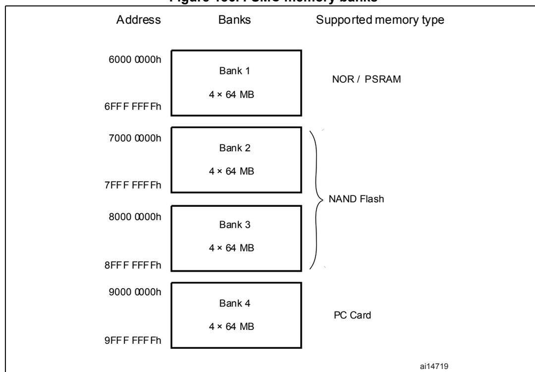
The diagram illustrates the memory banks and their address ranges:
| Address | Banks | Supported memory type |
|---|---|---|
| 6000 0000h | Bank 1 4 × 64 MB | NOR / PSRAM |
| 6FFF FFFFh | ||
| 7000 0000h | Bank 2 4 × 64 MB | NAND Flash |
| 7FFF FFFFh | ||
| 8000 0000h | Bank 3 4 × 64 MB | |
| 8FFF FFFFh | ||
| 9000 0000h | Bank 4 4 × 64 MB | PC Card |
| 9FFF FFFFh |
ai14719
21.4.1 NOR/PSRAM address mapping
HADDR[27:26] bits are used to select one of the four memory banks as shown in Table 100 .
Table 100. NOR/PSRAM bank selection
| HADDR[27:26] (1) | Selected bank |
|---|---|
| 00 | Bank 1 - NOR/PSRAM 1 |
| 01 | Bank 1 - NOR/PSRAM 2 |
| HADDR[27:26] (1) | Selected bank |
|---|---|
| 10 | Bank 1 - NOR/PSRAM 3 |
| 11 | Bank 1 - NOR/PSRAM 4 |
- 1. HADDR are internal AHB address lines that are translated to external memory.
HADDR[25:0] contain the external memory address. Since HADDR is a byte address whereas the memory is addressed in words, the address actually issued to the memory varies according to the memory data width, as shown in the following table.
Table 101. External memory address| Memory width (1) | Data address issued to the memory | Maximum memory capacity (bits) |
|---|---|---|
| 8-bit | HADDR[25:0] | 64 Mbyte x 8 = 512 Mbit |
| 16-bit | HADDR[25:1] >> 1 | 64 Mbyte/2 x 16 = 512 Mbit |
- 1. In case of a 16-bit external memory width, the FSMC will internally use HADDR[25:1] to generate the address for external memory FSMC_A[24:0].
Whatever the external memory width (16-bit or 8-bit), FSMC_A[0] should be connected to external memory address A[0].
Wrap support for NOR Flash/PSRAM
Wrap burst mode for synchronous memories is not supported. The memories must be configured in linear burst mode of undefined length.
21.4.2 NAND/PC Card address mapping
In this case, three banks are available, each of them divided into memory spaces as indicated in Table 102 .
Table 102. Memory mapping and timing registers| Start address | End address | FSMC Bank | Memory space | Timing register |
|---|---|---|---|---|
| 0x9C00 0000 | 0x9FFF FFFF | Bank 4 - PC card | I/O | FSMC_PIO4 (0xB0) |
| 0x9800 0000 | 0x9BFF FFFF | Attribute | FSMC_PATT4 (0xAC) | |
| 0x9000 0000 | 0x93FF FFFF | Common | FSMC_PMEM4 (0xA8) | |
| 0x8800 0000 | 0x8BFF FFFF | Bank 3 - NAND Flash | Attribute | FSMC_PATT3 (0x8C) |
| 0x8000 0000 | 0x83FF FFFF | Common | FSMC_PMEM3 (0x88) | |
| 0x7800 0000 | 0x7BFF FFFF | Bank 2 - NAND Flash | Attribute | FSMC_PATT2 (0x6C) |
| 0x7000 0000 | 0x73FF FFFF | Common | FSMC_PMEM2 (0x68) |
For NAND Flash memory, the common and attribute memory spaces are subdivided into three sections (see in Table 103 below) located in the lower 256 Kbytes:
- • Data section (first 64 Kbytes in the common/attribute memory space)
- • Command section (second 64 Kbytes in the common / attribute memory space)
- • Address section (next 128 Kbytes in the common / attribute memory space)
Table 103. NAND bank selections
| Section name | HADDR[17:16] | Address range |
|---|---|---|
| Address section | 1X | 0x020000-0x03FFFF |
| Command section | 01 | 0x010000-0x01FFFF |
| Data section | 00 | 0x000000-0x00FFFF |
The application software uses the 3 sections to access the NAND Flash memory:
- • To send a command to NAND Flash memory: the software must write the command value to any memory location in the command section.
- • To specify the NAND Flash address that must be read or written: the software must write the address value to any memory location in the address section. Since an address can be 4 or 5 bytes long (depending on the actual memory size), several consecutive writes to the address section are needed to specify the full address.
- • To read or write data: the software reads or writes the data value from or to any memory location in the data section.
Since the NAND Flash memory automatically increments addresses, there is no need to increment the address of the data section to access consecutive memory locations.
21.5 NOR Flash/PSRAM controller
The FSMC generates the appropriate signal timings to drive the following types of memories:
- • Asynchronous SRAM and ROM
- – 8-bit
- – 16-bit
- – 32-bit
- • PSRAM (Cellular RAM)
- – Asynchronous mode
- – Burst mode for synchronous accesses
- • NOR Flash
- – Asynchronous mode
- – Burst mode for synchronous accesses
- – Multiplexed or nonmultiplexed
The FSMC outputs a unique chip select signal NE[4:1] per bank. All the other signals (addresses, data and control) are shared.
For synchronous accesses, the FSMC issues the clock (CLK) to the selected external device only during the read/write transactions. This clock is a submultiple of the HCLK clock. The size of each bank is fixed and equal to 64 Mbytes.
Each bank is configured by means of dedicated registers (see Section 21.5.6 ).
The programmable memory parameters include access timings (see Table 104 ) and support for wait management (for PSRAM and NOR Flash accessed in burst mode).
Table 104. Programmable NOR/PSRAM access parameters| Parameter | Function | Access mode | Unit | Min. | Max. |
|---|---|---|---|---|---|
| Address setup | Duration of the address setup phase | Asynchronous | AHB clock cycle (HCLK) | 1 | 16 |
| Address hold | Duration of the address hold phase | Asynchronous, muxed I/Os | AHB clock cycle (HCLK) | 2 | 16 |
| Data setup | Duration of the data setup phase | Asynchronous | AHB clock cycle (HCLK) | 2 | 256 |
| Bus turn | Duration of the bus turnaround phase | Asynchronous and synchronous read/write | AHB clock cycle (HCLK) | 1 | 16 |
| Clock divide ratio | Number of AHB clock cycles (HCLK) to build one memory clock cycle (CLK) | Synchronous | AHB clock cycle (HCLK) | 2 | 16 |
| Data latency | Number of clock cycles to issue to the memory before the first data of the burst | Synchronous | Memory clock cycle (CLK) | 2 | 17 |
21.5.1 External memory interface signals
Table 105 , Table 106 and Table 107 list the signals that are typically used to interface NOR Flash, SRAM and PSRAM.
Note: Prefix “N”. specifies the associated signal as active low.
NOR Flash, nonmultiplexed I/Os
Table 105. Nonmultiplexed I/O NOR Flash| FSMC signal name | I/O | Function |
|---|---|---|
| CLK | O | Clock (for synchronous access) |
| A[25:0] | O | Address bus |
| D[15:0] | I/O | Bidirectional data bus |
| NE[x] | O | Chip select, x = 1..4 |
| NOE | O | Output enable |
| NWE | O | Write enable |
| NL(=NADV) | O | Latch enable (this signal is called address valid, NADV, by some NOR Flash devices) |
| NWAIT | I | NOR Flash wait input signal to the FSMC |
NOR Flash memories are addressed in 16-bit words. The maximum capacity is 512 Mbit (26 address lines).
NOR Flash, multiplexed I/Os
Table 106. Multiplexed I/O NOR Flash
| FSMC signal name | I/O | Function |
|---|---|---|
| CLK | O | Clock (for synchronous access) |
| A[25:16] | O | Address bus |
| AD[15:0] | I/O | 16-bit multiplexed, bidirectional address/data bus |
| NE[x] | O | Chip select, x = 1..4 |
| NOE | O | Output enable |
| NWE | O | Write enable |
| NL(=NADV) | O | Latch enable (this signal is called address valid, NADV, by some NOR Flash devices) |
| NWAIT | I | NOR Flash wait input signal to the FSMC |
NOR-Flash memories are addressed in 16-bit words. The maximum capacity is 512 Mbit (26 address lines).
PSRAM/SRAM
Table 107. Nonmultiplexed I/Os PSRAM/SRAM
| FSMC signal name | I/O | Function |
|---|---|---|
| CLK | O | Clock (only for PSRAM synchronous access) |
| A[25:0] | O | Address bus |
| D[15:0] | I/O | Data bidirectional bus |
| NE[x] | O | Chip select, x = 1..4 (called NCE by PSRAM (Cellular RAM i.e. CRAM)) |
| NOE | O | Output enable |
| NWE | O | Write enable |
| NL(= NADV) | O | Address valid only for PSRAM input (memory signal name: NADV) |
| NWAIT | I | PSRAM wait input signal to the FSMC |
| NBL[1] | O | Upper byte enable (memory signal name: NUB) |
| NBL[0] | O | Lowed byte enable (memory signal name: NLB) |
PSRAM memories are addressed in 16-bit words. The maximum capacity is 512 Mbit (26 address lines).
21.5.2 Supported memories and transactions
Table 108 below displays an example of the supported devices, access modes and transactions when the memory data bus is 16-bit for NOR, PSRAM and SRAM. Transactions not allowed (or not supported) by the FSMC in this example appear in gray.
Table 108. NOR Flash/PSRAM controller: example of supported memories and transactions
| Device | Mode | R/W | AHB data size | Memory data size | Allowed/not allowed | Comments |
|---|---|---|---|---|---|---|
| NOR Flash (muxed I/Os and nonmuxed I/Os) | Asynchronous | R | 8 | 16 | Y | - |
| Asynchronous | W | 8 | 16 | N | - | |
| Asynchronous | R | 16 | 16 | Y | - | |
| Asynchronous | W | 16 | 16 | Y | - | |
| Asynchronous | R | 32 | 16 | Y | Split into two FSMC accesses | |
| Asynchronous | W | 32 | 16 | Y | Split into two FSMC accesses | |
| Asynchronous page | R | - | 16 | N | Mode is not supported | |
| Synchronous | R | 8 | 16 | N | - | |
| Synchronous | R | 16 | 16 | Y | - | |
| Synchronous | R | 32 | 16 | Y | - | |
| PSRAM (multiplexed and nonmultiplexed I/Os) | Asynchronous | R | 8 | 16 | Y | - |
| Asynchronous | W | 8 | 16 | Y | Use of byte lanes NBL[1:0] | |
| Asynchronous | R | 16 | 16 | Y | - | |
| Asynchronous | W | 16 | 16 | Y | - | |
| Asynchronous | R | 32 | 16 | Y | Split into two FSMC accesses | |
| Asynchronous | W | 32 | 16 | Y | Split into two FSMC accesses | |
| Asynchronous page | R | - | 16 | N | Mode is not supported | |
| Synchronous | R | 8 | 16 | N | - | |
| Synchronous | R | 16 | 16 | Y | - | |
| Synchronous | R | 32 | 16 | Y | - | |
| Synchronous | W | 8 | 16 | Y | Use of byte lanes NBL[1:0] | |
| Synchronous | W | 16 / 32 | 16 | Y | - | |
| SRAM and ROM | Asynchronous | R | 8 / 16 | 16 | Y | - |
| Asynchronous | W | 8 / 16 | 16 | Y | Use of byte lanes NBL[1:0] | |
| Asynchronous | R | 32 | 16 | Y | Split into two FSMC accesses | |
| Asynchronous | W | 32 | 16 | Y | Split into two FSMC accesses. Use of byte lanes NBL[1:0] |
21.5.3 General timing rules
Signals synchronization
- • All controller output signals change on the rising edge of the internal clock (HCLK)
- • In synchronous mode (read or write), all output signals change on the rising edge of HCLK. Whatever the CLKDIV value, all outputs change as follows:
- – NOEL/NWEL/ NEL/NADVL/ NADVH /NBLL/ Address valid outputs change on the falling edge of FSMC_CLK clock.
- – NOEH/ NWEH / NEH/ NOEH/NBLH/ Address invalid outputs change on the rising edge of FSMC_CLK clock.
21.5.4 NOR Flash/PSRAM controller asynchronous transactions
Asynchronous static memories (NOR Flash memory, PSRAM, SRAM)
- • Signals are synchronized by the internal clock HCLK. This clock is not issued to the memory
- • The FSMC always samples the data before de-asserting the NOE signals. This guarantees that the memory data-hold timing constraint is met (chip enable high to data transition, usually 0 ns min.)
- • If the extended mode is enabled (EXTMOD bit is set in the FSMC_BCRx register), up to four extended modes (A, B, C and D) are available. It is possible to mix A, B, C and D modes for read and write operations. For example, read operation can be performed in mode A and write in mode B.
- • If the extended mode is disabled (EXTMOD bit is reset in the FSMC_BCRx register), the FSMC can operate in Mode1 or Mode2 as follows:
- – Mode 1 is the default mode when SRAM/PSRAM memory type is selected (MTYP[0:1] = 0x0 or 0x01 in the FSMC_BCRx register)
- – Mode 2 is the default mode when NOR memory type is selected (MTYP[0:1] = 0x10 in the FSMC_BCRx register).
Mode 1 - SRAM/PSRAM (CRAM)
The next figures show the read and write transactions for the supported modes followed by the required configuration of FSMC_BCRx, and FSMC_BTRx/FSMC_BWTRx registers.
Figure 187. Mode1 read accesses
![Timing diagram for Mode1 read accesses showing signals A[25:0], NBL[1:0], NEx, NOE, NWE, and D[15:0] over time. The diagram shows the sequence of a memory transaction with address, data, and control signals. Address A[25:0] and data bus D[15:0] are shown with setup and hold times. Control signals NEx and NOE are active-low, while NWE is active-low and held high. NBL[1:0] are driven low during the read. Timing parameters include (ADDSET + 1) HCLK cycles for address setup, (DATAST + 1) HCLK cycles for data setup, and 2 HCLK cycles for data hold. Data sampling and strobing occur on the falling edge of NOE.](/RM0008-STM32F101-102-103-105-107/b2b2f40716e2bc85fef3ad334ed43e4e_img.jpg)
- 1. NBL[1:0] are driven low during read access.
Figure 188. Mode1 write accesses
![Timing diagram for Mode1 write accesses showing signals A[25:0], NBL[1:0], NEx, NOE, NWE, and D[15:0] over time. The diagram shows the sequence of a memory transaction with address, data, and control signals. Address A[25:0] and data bus D[15:0] are shown with setup and hold times. Control signals NEx and NOE are active-low, while NWE is active-low and held high. NBL[1:0] are driven low during the write. Timing parameters include (ADDSET + 1) HCLK cycles for address setup, (DATAST + 1) HCLK cycles for data setup, and 1 HCLK cycle for data hold. Data is driven by FSMC. The rising edge of NWE occurs 1 HCLK cycle after the data is driven.](/RM0008-STM32F101-102-103-105-107/fbde6fe5e439bbc8e83a3bb6e0bff52e_img.jpg)
The one HCLK cycle at the end of the write transaction helps guarantee the address and data hold time after the NWE rising edge. Due to the presence of this one HCLK cycle, the DATAST value must be greater than zero (DATAST > 0).
Table 109. FSMC_BCRx bit fields
| Bit number | Bit name | Value to set |
|---|---|---|
| 31:20 | Reserved | 0x000 |
| 19 | CBURSTRW | 0x0 (no effect on asynchronous mode) |
| 18:16 | CPSIZE | 0x0 (no effect on asynchronous mode) |
| 15 | ASYNCWAIT | Set to 1 if the memory supports this feature. Otherwise keep at 0. |
| 14 | EXTMOD | 0x0 |
| 13 | WAITEN | 0x0 (no effect on asynchronous mode) |
| 12 | WREN | As needed |
| 11 | WAITCFG | Don't care |
| 10 | WRAPMOD | 0x0 |
| 9 | WAITPOL | Meaningful only if bit 15 is 1 |
| 8 | BURSTEN | 0x0 |
| 7 | Reserved | 0x1 |
| 6 | FACCEN | Don't care |
| 5:4 | MWID | As needed |
| 3:2 | MTYP[0:1] | As needed, exclude 0x2 (NOR Flash) |
| 1 | MUXE | 0x0 |
| 0 | MBKEN | 0x1 |
Table 110. FSMC_BTRx bit fields
| Bit number | Bit name | Value to set |
|---|---|---|
| 31:30 | Reserved | 0x0 |
| 29:28 | ACCMOD | Don't care |
| 27:24 | DATLAT | Don't care |
| 23:20 | CLKDIV | Don't care |
| 19:16 | BUSTURN | Time between NEx high to NEx low (BUSTURN HCLK) |
| 15:8 | DATAST | Duration of the second access phase (DATAST+1 HCLK cycles for write accesses, DATAST+3 HCLK cycles for read accesses). This value cannot be 0 (minimum is 1). |
| 7:4 | ADDHLD | Don't care |
| 3:0 | ADDSET[3:0] | Duration of the first access phase (ADDSET+1 HCLK cycles). |
Mode A - SRAM/PSRAM (CRAM) OE toggling
Figure 189. ModeA read accesses
![Timing diagram for Mode A read accesses showing signals A[25:0], NBL[1:0], NEx, NOE, NWE, and D[15:0] over time. The diagram illustrates the memory transaction phases: address setup, data drive, data sampled, and data strobe. NBL[1:0] are driven low during the read access. Timing parameters include (ADDSET + 1) HCLK cycles for address setup, (DATAST + 1) HCLK cycles for data drive, and 2 HCLK cycles for data sampled and strobe.](/RM0008-STM32F101-102-103-105-107/87ad23a8be84808c31a4cc6edb67fa67_img.jpg)
Timing diagram for Mode A read accesses. The diagram shows the following signals and timing parameters:
- Signals:
- A[25:0]: Address bus, stable during the memory transaction.
- NBL[1:0]: Byte Lane signals, driven low during the read access.
- NEx: Chip Select signal, goes low at the start and high at the end of the transaction.
- NOE: Output Enable signal, goes low to enable data output and high to disable it.
- NWE: Write Enable signal, remains high throughout the read transaction.
- D[15:0]: Data bus, driven by memory during the data drive phase.
- Timing Parameters:
- (ADDSET + 1) HCLK cycles: Time from the start of the transaction to the falling edge of NOE.
- (DATAST + 1) HCLK cycles: Duration from the falling edge of NOE to the rising edge of NOE.
- 2 HCLK cycles: Time from the rising edge of NOE to the end of the memory transaction.
- Phases:
- Memory transaction: The overall duration of the read operation.
- data driven by memory: The phase where data is output from the memory to the bus.
- Data sampled: The point where the controller samples the data from the bus.
- Data strobe: The point where the data is latched.
ai14722c
- 1. NBL[1:0] are driven low during read access.
Figure 190. ModeA write accesses
![Timing diagram for Mode A write accesses showing signals A[25:0], NBL[1:0], NEx, NOE, NWE, and D[15:0] over time. The diagram illustrates the memory transaction phases: address setup and data drive. NWE goes low to enable writing. Timing parameters include (ADDSET + 1) HCLK cycles for address setup and (DATAST + 1) HCLK cycles for data drive. A 1HCLK cycle delay is shown between the start of the data drive phase and the falling edge of NWE.](/RM0008-STM32F101-102-103-105-107/58939d78fdd774388e595ef85aea2cfa_img.jpg)
Timing diagram for Mode A write accesses. The diagram shows the following signals and timing parameters:
- Signals:
- A[25:0]: Address bus, stable during the memory transaction.
- NBL[1:0]: Byte Lane signals, driven low during the write access.
- NEx: Chip Select signal, goes low at the start and high at the end of the transaction.
- NOE: Output Enable signal, remains high throughout the write transaction.
- NWE: Write Enable signal, goes low to enable writing and high to disable it.
- D[15:0]: Data bus, driven by FSMC during the data drive phase.
- Timing Parameters:
- (ADDSET + 1) HCLK cycles: Time from the start of the transaction to the falling edge of NWE.
- (DATAST + 1) HCLK cycles: Duration from the falling edge of NWE to the rising edge of NWE.
- 1HCLK: Time from the rising edge of NWE to the end of the memory transaction.
- Phases:
- Memory transaction: The overall duration of the write operation.
- data driven by FSMC: The phase where data is output from the FSMC to the bus.
ai14721c
The differences compared with mode1 are the toggling of NOE and the independent read and write timings.
Table 111. FSMC_BCRx bit fields
| Bit number | Bit name | Value to set |
|---|---|---|
| 31-20 | Reserved | 0x000 |
| 19 | CBURSTRW | 0x0 (no effect on asynchronous mode) |
| 18:16 | CPSIZE | 0x0 (no effect on asynchronous mode) |
| 15 | ASYNCWAIT | Set to 1 if the memory supports this feature. Otherwise keep at 0. |
| 14 | EXTMOD | 0x1 |
| 13 | WAITEN | 0x0 (no effect on asynchronous mode) |
| 12 | WREN | As needed |
| 11 | WAITCFG | Don't care |
| 10 | WRAPMOD | 0x0 |
| 9 | WAITPOL | Meaningful only if bit 15 is 1 |
| 8 | BURSTEN | 0x0 |
| 7 | Reserved | 0x1 |
| 6 | FACCEN | Don't care |
| 5-4 | MWID | As needed |
| 3-2 | MTYP[0:1] | As needed, exclude 0x2 (NOR Flash) |
| 1 | MUXEN | 0x0 |
| 0 | MBKEN | 0x1 |
Table 112. FSMC_BTRx bit fields
| Bit number | Bit name | Value to set |
|---|---|---|
| 31:30 | Reserved | 0x0 |
| 29-28 | ACCMOD | 0x0 |
| 27-24 | DATLAT | Don't care |
| 23-20 | CLKDIV | Don't care |
| 19-16 | BUSTURN | Time between NEx high to NEx low (BUSTURN HCLK) |
| 15-8 | DATAST | Duration of the second access phase (DATAST+3 HCLK cycles) for read accesses. This value cannot be 0 (minimum is 1). |
| 7-4 | ADDHLD | Don't care |
| 3-0 | ADDSET[3:0] | Duration of the first access phase (ADDSET+1 HCLK cycles) for read accesses. |
Table 113. FSMC_BWTRx bit fields
| Bit number | Bit name | Value to set |
|---|---|---|
| 31:30 | Reserved | 0x0 |
| 29:28 | ACCMOD | 0x0 |
| 27:24 | DATLAT | Don't care |
| 23:20 | CLKDIV | Don't care |
| 19:16 | BUSTURN | Time between NEx high to NEx low (BUSTURN HCLK) |
| 15:8 | DATAST | Duration of the second access phase (DATAST+1 HCLK cycles for write accesses, DATAST+3 HCLK cycles for read accesses). This value cannot be 0 (minimum is 1). |
| 7-4 | ADDHLD | Don't care |
| 3-0 | ADDSET[3:0] | Duration of the first access phase (ADDSET+1 HCLK cycles) for write accesses. |
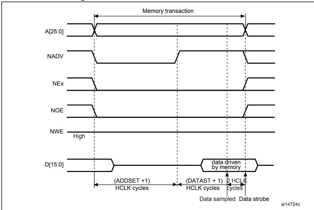
Mode 2/B - NOR Flash
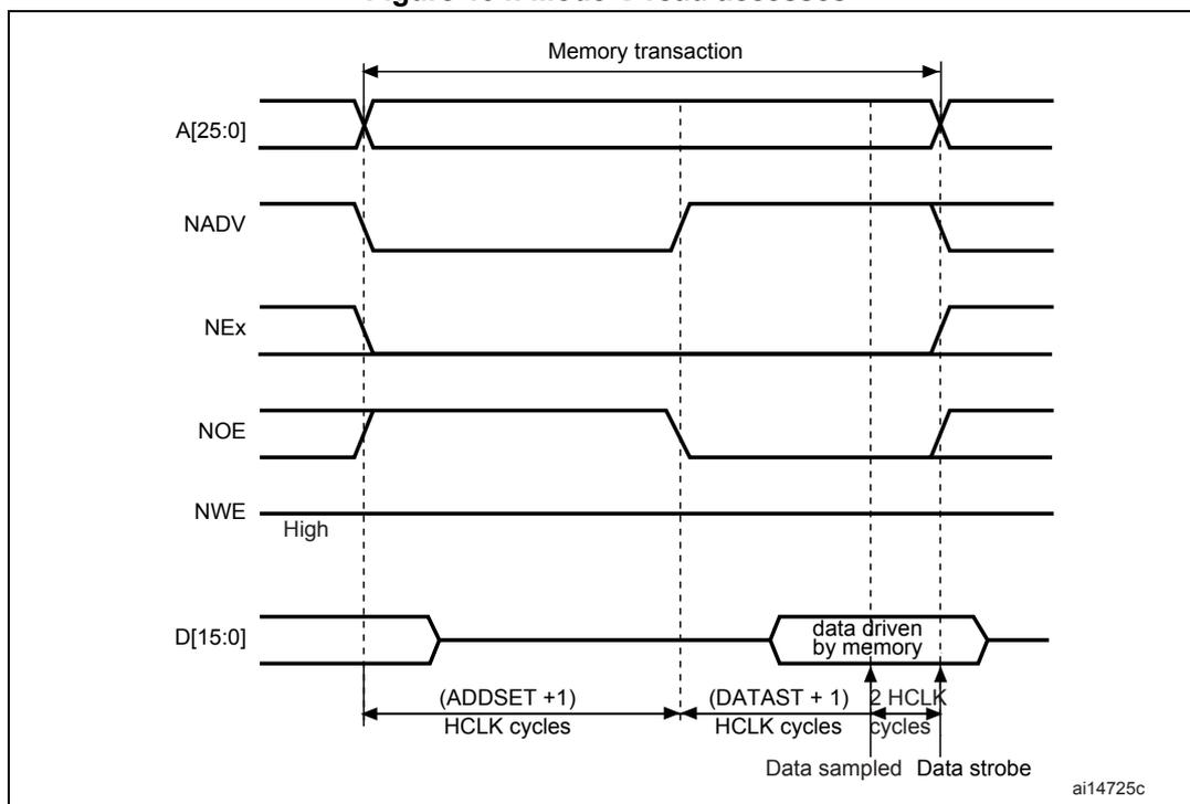
Figure 191. Mode2 and mode B read accesses
The diagram illustrates the timing for Mode 2 and Mode B read accesses. The address lines A[25:0] are stable during the memory transaction. The NADV signal is active-low and goes low at the start of the transaction. The NEx signal is active-low and goes low at the start of the transaction. The NOE signal is active-low and goes low at the start of the transaction. The NWE signal is active-high and remains high throughout the transaction. The data bus D[15:0] is driven by memory during the second access phase. The first access phase duration is (ADDSET + 1) HCLK cycles. The second access phase duration is (DATAST + 1) HCLK cycles. Data is sampled 2 HCLK cycles after the start of the second access phase. The data strobe is generated 2 HCLK cycles after the start of the second access phase.
Figure 192. Mode2 write accesses
![Timing diagram for Mode2 write accesses showing signals A[25:0], NADV, NEx, NOE, NWE, and D[15:0] over time. The diagram illustrates the memory transaction phases: address setup and data drive. Timings are defined in HCLK cycles: (ADDSET + 1) for address setup and (DATAST + 1) for data drive. A 1HCLK cycle is also indicated between NOE and NWE toggling. Reference code ai14723b is present in the bottom right.](/RM0008-STM32F101-102-103-105-107/b3f1506ad14a0a0b6260fee886e282b1_img.jpg)
Figure 193. Mode B write accesses
![Timing diagram for Mode B write accesses, similar to Figure 192 but with different signal toggling and timing parameters. It shows signals A[25:0], NADV, NEx, NOE, NWE, and D[15:0]. Timings are (ADDSET + 1) HCLK cycles for address setup and (DATAST + 1) HCLK cycles for data drive. Reference code ai15110b is present in the bottom right.](/RM0008-STM32F101-102-103-105-107/569180d3a335978551f9c352ba26f485_img.jpg)
The differences with mode1 are the toggling of NWE and the independent read and write timings when extended mode is set (Mode B).
Table 114. FSMC_BCRx bit fields
| Bit number | Bit name | Value to set |
|---|---|---|
| 31-20 | Reserved | 0x000 |
| 19 | CBURSTRW | 0x0 (no effect on asynchronous mode) |
| 18:16 | Reserved | 0x0 (no effect on asynchronous mode) |
| 15 | ASYNCWAIT | Set to 1 if the memory supports this feature. Otherwise keep at 0. |
| 14 | EXTMOD | 0x1 for mode B, 0x0 for mode 2 |
| 13 | WAITEN | 0x0 (no effect on asynchronous mode) |
| 12 | WREN | As needed |
| 11 | WAITCFG | Don't care |
| 10 | WRAPMOD | 0x0 |
| 9 | WAITPOL | Meaningful only if bit 15 is 1 |
| 8 | BURSTEN | 0x0 |
| 7 | Reserved | 0x1 |
| 6 | FACCEN | 0x1 |
| 5-4 | MWID | As needed |
| 3-2 | MTYP[0:1] | 0x2 (NOR Flash memory) |
| 1 | MUXEN | 0x0 |
| 0 | MBKEN | 0x1 |
Table 115. FSMC_BTRx bit fields
| Bit number | Bit name | Value to set |
|---|---|---|
| 31:30 | Reserved | 0x0 |
| 29:28 | ACCMOD | 0x1 |
| 27:24 | DATLAT | Don't care |
| 23:20 | CLKDIV | Don't care |
| 19:16 | BUSTURN | Time between NEx high to NEx low (BUSTURN HCLK) |
| 15-8 | DATAST | Duration of the second access phase (DATAST+3 HCLK cycles) for read accesses. This value cannot be 0 (minimum is 1). |
| 7-4 | ADDHLD | Don't care |
| 3-0 | ADDSET[3:0] | Duration of the first access phase (ADDSET+1 HCLK cycles) for read accesses. |
Table 116. FSMC_BWTRx bit fields
| Bit number | Bit name | Value to set |
|---|---|---|
| 31:30 | Reserved | 0x0 |
| 29:28 | ACCMOD | 0x1 |
| 27:24 | DATLAT | Don't care |
| 23:20 | CLKDIV | Don't care |
| 19:16 | BUSTURN | Time between NEx high to NEx low (BUSTURN HCLK) |
| 15:8 | DATAST | Duration of the second access phase (DATAST+1 HCLK cycles for write accesses, DATAST+3 HCLK cycles for write accesses). This value cannot be 0 (minimum is 1). |
| 7:4 | ADDHLD | Don't care |
| 3:0 | ADDSET[3:0] | Duration of the first access phase (ADDSET+1 HCLK cycles) for write accesses. |
Note: The FSMC_BWTRx register is valid only if extended mode is set (mode B), otherwise all its content is don't care.
Mode C - NOR Flash - OE toggling
Figure 194. Mode C read accesses
The diagram illustrates the timing for a read access in Mode C. The address A[25:0] is stable during the entire memory transaction. The NADV signal goes low to indicate valid address and data, and goes high at the end of the transaction. The NEx signal goes low to start the transaction and goes high at the end. The NOE signal goes low to enable data output from the memory. The NWE signal remains high throughout. The data D[15:0] is driven by memory when NOE is low. The diagram is divided into three phases: the first access phase of (ADDSET + 1) HCLK cycles, the second access phase of (DATAST + 1) HCLK cycles, and a 2 HCLK cycle phase where data is sampled and strobed. Vertical dashed lines mark the boundaries between these phases.
Figure 195. Mode C write accesses
![Timing diagram for Mode C write accesses showing address (A[25:0]), NADV, NEx, NOE, NWE, and data (D[15:0]) signals over time. The diagram shows the 'Memory transaction' period, 'data driven by FSMC' phase, and timing parameters: (ADDSET + 1) HCLK cycles and (DATAST + 1) HCLK cycles. A 1HCLK cycle is also indicated between NOE and NWE transitions.](/RM0008-STM32F101-102-103-105-107/9b52d22a97ce7e5a37943d5052db7f5e_img.jpg)
The differences compared with mode1 are the toggling of NOE and the independent read and write timings.
Table 117. FSMC_BCRx bit fields
| Bit No. | Bit name | Value to set |
|---|---|---|
| 31-20 | Reserved | 0x000 |
| 19 | CBURSTRW | 0x0 (no effect on asynchronous mode) |
| 18:16 | CPSIZE | 0x0 (no effect on asynchronous mode) |
| 15 | ASYNCWAIT | Set to 1 if the memory supports this feature. Otherwise keep at 0. |
| 14 | EXTMOD | 0x1 |
| 13 | WAITEN | 0x0 (no effect on asynchronous mode) |
| 12 | WREN | As needed |
| 11 | WAITCFG | Don't care |
| 10 | WRAPMOD | 0x0 |
| 9 | WAITPOL | Meaningful only if bit 15 is 1 |
| 8 | BURSTEN | 0x0 |
| 7 | Reserved | 0x1 |
| 6 | FACCEN | 0x1 |
| 5-4 | MWID | As needed |
| 3-2 | MTYP[0:1] | 0x2 (NOR Flash memory) |
| Bit No. | Bit name | Value to set |
|---|---|---|
| 1 | MUXEN | 0x0 |
| 0 | MBKEN | 0x1 |
| Bit number | Bit name | Value to set |
|---|---|---|
| 31:30 | Reserved | 0x0 |
| 29:28 | ACCMOD | 0x2 |
| 27:24 | DATLAT | 0x0 |
| 23:20 | CLKDIV | 0x0 |
| 19:16 | BUSTURN | Time between NEx high to NEx low (BUSTURN HCLK) |
| 15:8 | DATAST | Duration of the second access phase (DATAST+3 HCLK cycles) for read accesses. This value cannot be 0 (minimum is 1). |
| 7:4 | ADDHLD | Don't care |
| 3:0 | ADDSET[3:0] | Duration of the first access phase (ADDSET+1 HCLK cycles) for read accesses. |
| Bit number | Bit name | Value to set |
|---|---|---|
| 31:30 | Reserved | 0x0 |
| 29:28 | ACCMOD | 0x2 |
| 27:24 | DATLAT | Don't care |
| 23:20 | CLKDIV | Don't care |
| 19:16 | BUSTURN | Time between NEx high to NEx low (BUSTURN HCLK) |
| 15:8 | DATAST | Duration of the second access phase (DATAST+1 HCLK cycles for write accesses, DATAST+3 HCLK cycles for write accesses). This value cannot be 0 (minimum is 1). |
| 7:4 | ADDHLD | Don't care |
| 3:0 | ADDSET[3:0] | Duration of the first access phase (ADDSET+1 HCLK cycles) for write accesses. |
Mode D - asynchronous access with extended address
Figure 196. Mode D read accesses
![Timing diagram for Mode D read accesses showing signals A[25:0], NADV, NEx, NOE, NWE, and D[15:0] over time. It details the memory transaction phases and timing parameters like ADDSET, ADDHLD, and DATAST in HCLK cycles.](/RM0008-STM32F101-102-103-105-107/19002ea9fbefd66cc31127c56ac9475a_img.jpg)
This timing diagram illustrates the sequence of signals for a read access in Mode D. The signals shown are address lines A[25:0], address latch strobe NADV, next address strobe NEx, output enable NOE, write enable NWE (held High), and data lines D[15:0]. The diagram is divided into three main timing intervals: (ADDSET + 1) HCLK cycles for address setup, (ADDHLD + 1) HCLK cycles for address hold, and (DATAST + 1) HCLK cycles for data strobe. The data is driven by memory and is sampled 2 HCLK cycles after the data strobe is asserted. The entire sequence is labeled as a "Memory transaction".
Figure 197. Mode D write accesses
![Timing diagram for Mode D write accesses showing signals A[25:0], NADV, NEx, NOE, NWE, and D[15:0] over time. It details the memory transaction phases and timing parameters like ADDSET, ADDHLD, and DATAST in HCLK cycles, with data driven by FSMC.](/RM0008-STM32F101-102-103-105-107/62d347964ceb3e12507749ca14dcfa32_img.jpg)
This timing diagram illustrates the sequence of signals for a write access in Mode D. The signals shown are the same as in the read diagram. The timing intervals for address setup (ADDSET + 1) and address hold (ADDHLD + 1) HCLK cycles are identical. The data, driven by the FSMC, is sampled (DATAST + 1) HCLK cycles after the address hold begins. The write enable signal NWE is then asserted for a duration of 1HCLK cycle.
The differences with mode1 are the toggling of NOE that goes on toggling after NADV changes and the independent read and write timings.
Table 120. FSMC_BCRx bit fields
| Bit No. | Bit name | Value to set |
|---|---|---|
| 31-20 | Reserved | 0x000 |
| 19 | CBURSTRW | 0x0 (no effect on asynchronous mode) |
| 18:16 | CPSIZE | 0x0 (no effect on asynchronous mode) |
| 15 | ASYNCWAIT | Set to 1 if the memory supports this feature. Otherwise keep at 0. |
| 14 | EXTMOD | 0x1 |
| 13 | WAITEN | 0x0 (no effect on asynchronous mode) |
| 12 | WREN | As needed |
| 11 | WAITCFG | Don't care |
| 10 | WRAPMOD | 0x0 |
| 9 | WAITPOL | Meaningful only if bit 15 is 1 |
| 8 | BURSTEN | 0x0 |
| 7 | Reserved | 0x1 |
| 6 | FACCEN | Set according to memory support |
| 5-4 | MWID | As needed |
| 3-2 | MTYP[0:1] | As needed |
| 1 | MUXEN | 0x0 |
| 0 | MBKEN | 0x1 |
Table 121. FSMC_BTRx bit fields
| Bit No. | Bit name | Value to set |
|---|---|---|
| 31:30 | Reserved | 0x0 |
| 29-28 | ACCMOD | 0x3 |
| 27-24 | DATLAT | Don't care |
| 23-20 | CLKDIV | Don't care |
| 19-16 | BUSTURN | Time between NEx high to NEx low (BUSTURN HCLK) |
| 15-8 | DATAST | Duration of the second access phase (DATAST+3 HCLK cycles) for read accesses. This value cannot be 0 (minimum is 1) |
| 7-4 | ADDHLD | Duration of the middle phase of the read access (ADDHLD+1 HCLK cycles) |
| 3-0 | ADDSET[3:0] | Duration of the first access phase (ADDSET+1 HCLK cycles) for read accesses. |
Table 122. FSMC_BWTRx bit fields
| Bit No. | Bit name | Value to set |
|---|---|---|
| 31:30 | Reserved | 0x0 |
| 29:28 | ACCMOD | 0x3 |
| 27:24 | DATLAT | 0x0 |
| 23:20 | CLKDIV | 0x0 |
| 19:16 | BUSTURN | Time between NEx high to NEx low (BUSTURN HCLK) |
| 15:8 | DATAST | Duration of the second access phase (DATAST+3 HCLK cycles) for write accesses. This value cannot be 0 (minimum is 1) |
| 7:4 | ADDHLD | Duration of the middle phase of the write access (ADDHLD+1 HCLK cycles) |
| 3:0 | ADDSET[3:0] | Duration of the first access phase (ADDSET+1 HCLK cycles) for write accesses. |
Muxed mode - multiplexed asynchronous access to NOR Flash memory
Figure 198. Multiplexed read accesses
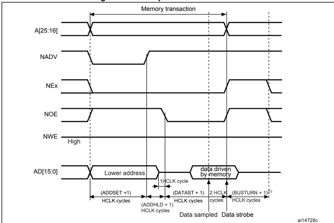
The diagram illustrates the timing for multiplexed read accesses. The address lines A[25:16] are active during the first access phase. The address strobe NADV is active low. The memory address NEx is active low. The data output enable NOE is active low. The data lines AD[15:0] are multiplexed, carrying lower address information during the first access phase and data driven by memory during the second access phase. The write enable NWE is high. The timing parameters are defined as follows:
- ADDSET + 1 : Duration of the first access phase in HCLK cycles.
- ADDHLD + 1 : Duration of the middle phase in HCLK cycles.
- 1 HCLK cycle : The duration of a single clock cycle.
- DATAST + 1 : Duration of the second access phase in HCLK cycles.
- 2 HCLK cycles : The duration of the data sampling phase.
- BUSTURN + 1 : The bus turnaround delay in HCLK cycles.
1. The bus turnaround delay (BUSTURN + 1) and the delay between side-by-side transactions overlap, so BUSTURN \( \leq \) 5 has no impact.
Figure 199. Multiplexed write accesses
![Timing diagram for multiplexed write accesses. The diagram shows the relationship between address lines A[25:16], control signals NADV, NEx, NOE, NWE, and data lines AD[15:0] during a memory transaction. The transaction is divided into three phases: address setup, address hold, and data drive. The address setup phase lasts (ADDSET + 1) HCLK cycles. The address hold phase lasts ADDHLD HCLK cycles. The data drive phase lasts (DATAST + 2) HCLK cycles. The NADV signal is active low and goes low during the address setup phase. The NEx signal is active low and goes low during the address setup phase. The NOE signal is active low and goes low during the data drive phase. The NWE signal is active low and goes low during the data drive phase. The AD[15:0] lines are driven by the FSMC during the data drive phase. A 1HCLK cycle is indicated between the address hold and data drive phases.](/RM0008-STM32F101-102-103-105-107/361383266b590c98699aadaf99fd77d3_img.jpg)
Timing diagram for multiplexed write accesses. The diagram shows the relationship between address lines A[25:16], control signals NADV, NEx, NOE, NWE, and data lines AD[15:0] during a memory transaction. The transaction is divided into three phases: address setup, address hold, and data drive. The address setup phase lasts (ADDSET + 1) HCLK cycles. The address hold phase lasts ADDHLD HCLK cycles. The data drive phase lasts (DATAST + 2) HCLK cycles. The NADV signal is active low and goes low during the address setup phase. The NEx signal is active low and goes low during the address setup phase. The NOE signal is active low and goes low during the data drive phase. The NWE signal is active low and goes low during the data drive phase. The AD[15:0] lines are driven by the FSMC during the data drive phase. A 1HCLK cycle is indicated between the address hold and data drive phases.
The difference with mode D is the drive of the lower address byte(s) on the databus.
Table 123. FSMC_BCRx bit fields
| Bit No. | Bit name | Value to set |
|---|---|---|
| 31-21 | Reserved | 0x000 |
| 19 | CBURSTRW | 0x0 (no effect on asynchronous mode) |
| 18:16 | CPSIZE | 0x0 (no effect on asynchronous mode) |
| 15 | ASYNCWAIT | Set to 1 if the memory supports this feature. Otherwise keep at 0. |
| 14 | EXTMOD | 0x0 |
| 13 | WAITEN | 0x0 (no effect on asynchronous mode) |
| 12 | WREN | As needed |
| 11 | WAITCFG | Don't care |
| 10 | WRAPMOD | 0x0 |
| 9 | WAITPOL | Meaningful only if bit 15 is 1 |
| 8 | BURSTEN | 0x0 |
| 7 | Reserved | 0x1 |
| 6 | FACCEN | 0x1 |
| Bit No. | Bit name | Value to set |
|---|---|---|
| 5-4 | MWID | As needed |
| 3-2 | MTYP[0:1] | 0x2 (NOR Flash memory) |
| 1 | MUXEN | 0x1 |
| 0 | MBKEN | 0x1 |
| Bit No. | Bit name | Value to set |
|---|---|---|
| 31:30 | Reserved | 0x0 |
| 29-28 | ACCMOD | 0x0 |
| 27-24 | DATLAT | Don't care |
| 23-20 | CLKDIV | Don't care |
| 19-16 | BUSTURN | Duration of the last phase of the access (BUSTURN+1 HCLK) |
| 15-8 | DATAST | Duration of the second access phase (DATAST+3 HCLK cycles for read accesses and DATAST+1 HCLK cycles for write accesses). This value cannot be 0 (minimum is 1) |
| 7-4 | ADDHLD | Duration of the middle phase of the access (ADDHLD+1 HCLK cycles). This value cannot be 0 (minimum is 1). |
| 3-0 | ADDSET[3:0] | Duration of the first access phase (ADDSET+1 HCLK cycles). |
WAIT management in asynchronous accesses
If the asynchronous memory asserts a WAIT signal to indicate that it is not yet ready to accept or to provide data, the ASYNCWAIT bit has to be set in FSMC_BCRx register.
If the WAIT signal is active (high or low depending on the WAITPOL bit), the second access phase (Data setup phase) programmed by the DATAST bits, is extended until WAIT becomes inactive. Unlike the data setup phase, the first access phases (Address setup and Address hold phases), programmed by the ADDSET[3:0] and ADDHLD bits, are not WAIT sensitive and so they are not prolonged.
The data setup phase (DATAST in FSMC_BTRx register) must be programmed so that the WAIT signal meets the following conditions:
- • For read accesses: WAIT can be detected 4 HCLK cycles before data is being sampled or 6 HCLK cycles before NOE is deasserted (refer to Figure 200 ).
- • For write accesses: WAIT can be detected 4 HCLK cycles before NWE deassertion (refer to Figure 201 ).
- 1. Memory asserts the WAIT signal aligned to NOE/NWE which toggles:
- 2. Memory asserts the WAIT signal aligned to NEx (or NOE/NWE not toggling):
if
then
otherwise
where \( \max\_wait\_assertion\_time \) is the maximum time taken by the memory to assert the WAIT signal once NEx/NOE/NWE is low.
Figure 200 and Figure 201 show the number of HCLK clock cycles that are added to the memory access after WAIT is released by the asynchronous memory (independently of the above cases).
Figure 200. Asynchronous wait during a read access
![Timing diagram for asynchronous wait during a read access. The diagram shows five signal lines: A[25:0] (Address), NEx (Active-low memory address strobe), NWAIT (Asynchronous wait signal), NOE (Active-low output enable), and D[15:0] (Data bus). The timing is divided into three phases: 'address phase', 'data setup phase', and 'Memory transaction'. The address phase starts with a falling edge of NEx and ends with a rising edge of NEx. The data setup phase starts with a falling edge of NEx and ends with a rising edge of NEx. The NWAIT signal is shown as 'don't care' during the address and data setup phases, and as a low signal during the data setup phase. The NOE signal is shown as a low signal during the data setup phase. The data bus D[15:0] is shown as 'data driven by memory' during the data setup phase. The data is sampled at the rising edge of HCLK, which is shown as a vertical dashed line. The data setup phase is divided into two segments: '4HCLK' and '2HCLK'. The diagram is labeled 'ai15796c' in the bottom right corner.](/RM0008-STM32F101-102-103-105-107/847d6b99e49c91da3099835e34db0eaf_img.jpg)
- 1. NWAIT polarity depends on WAITPOL bit setting in FSMC_BCRx register.
Figure 201. Asynchronous wait during a write access
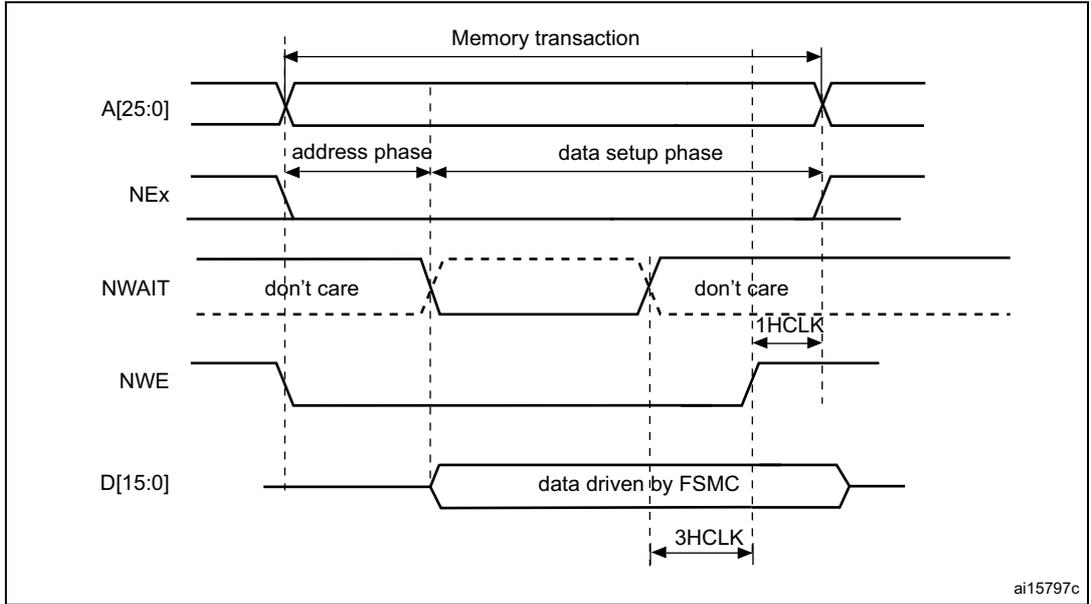
The diagram displays the following signals and their states:
- A[25:0] : Address bus. It transitions at the start of the address phase and remains stable until the end of the data setup phase.
- NEx : Chip select signal. It goes low at the start of the address phase and returns high at the end of the data setup phase.
- NWAIT : Wait signal. It is shown with 'don't care' regions. It transitions from high to low at the end of the address phase and returns high during the data setup phase. A dashed line indicates an alternative state. A timing interval of 1HCLK is marked at its rising edge.
- NWE : Write enable signal. It goes low at the start of the address phase and returns high at the end of the data setup phase.
- D[15:0] : Data bus. It is 'data driven by FSMC' starting from the beginning of the data setup phase for a duration of 3HCLK.
The total 'Memory transaction' spans from the start of the address phase to the end of the data setup phase.
ai15797c
- 1. NWAIT polarity depends on WAITPOL bit setting in FSMC_BCRx register.
21.5.5 Synchronous transactions
The memory clock, CLK, is a submultiple of HCLK according to the value of parameter CLKDIV.
NOR Flash memories specify a minimum time from NADV assertion to CLK high. To meet this constraint, the FSMC does not issue the clock to the memory during the first internal clock cycle of the synchronous access (before NADV assertion). This guarantees that the rising edge of the memory clock occurs in the middle of the NADV low pulse.
Data latency versus NOR Flash latency
The data latency is the number of cycles to wait before sampling the data. The DATLAT value must be consistent with the latency value specified in the NOR Flash configuration register. The FSMC does not include the clock cycle when NADV is low in the data latency count.
Caution: Some NOR Flash memories include the NADV Low cycle in the data latency count, so the exact relation between the NOR Flash latency and the FSMC DATLAT parameter can be either of:
- • NOR Flash latency = (DATLAT + 2) CLK clock cycles
- • NOR Flash latency = (DATLAT + 3) CLK clock cycles
Some recent memories assert NWAIT during the latency phase. In such cases DATLAT can be set to its minimum value. As a result, the FSMC samples the data and waits long enough to evaluate if the data are valid. Thus the FSMC detects when the memory exits latency and real data are taken.
Other memories do not assert NWAIT during latency. In this case the latency must be set correctly for both the FSMC and the memory, otherwise invalid data are mistaken for good data, or valid data are lost in the initial phase of the memory access.
Single-burst transfer
When the selected bank is configured in burst mode for synchronous accesses, if for example an AHB single-burst transaction is requested on 16-bit memories, the FSMC performs a burst transaction of length 1 (if the AHB transfer is 16-bit), or length 2 (if the AHB transfer is 32-bit) and de-assert the chip select signal when the last data is strobed.
Clearly, such a transfer is not the most efficient in terms of cycles (compared to an asynchronous read). Nevertheless, a random asynchronous access would first require to re-program the memory access mode, which would altogether last longer.
Cross boundary page for Cellular RAM 1.5
Cellular RAM 1.5 does not allow burst access to cross the page boundary. The FSMC controller allows to split automatically the burst access when the memory page size is reached by configuring the CPSIZE bits in the FSMC_BCR1 register following the memory page size.
Wait management
For synchronous NOR Flash memories, NWAIT is evaluated after the programmed latency period, (DATLAT+2) CLK clock cycles.
If NWAIT is sensed active (low level when WAITPOL = 0, high level when WAITPOL = 1), wait states are inserted until NWAIT is sensed inactive (high level when WAITPOL = 0, low level when WAITPOL = 1).
When NWAIT is inactive, the data is considered valid either immediately (bit WAITCFG = 1) or on the next clock edge (bit WAITCFG = 0).
During wait-state insertion via the NWAIT signal, the controller continues to send clock pulses to the memory, keeping the chip select and output enable signals valid, and does not consider the data valid.
There are two timing configurations for the NOR Flash NWAIT signal in burst mode:
- • Flash memory asserts the NWAIT signal one data cycle before the wait state (default after reset)
- • Flash memory asserts the NWAIT signal during the wait state
These two NOR Flash wait state configurations are supported by the FSMC, individually for each chip select, thanks to the WAITCFG bit in the FSMC_BCRx registers (x = 0..3).
Figure 202. Wait configurations
![Timing diagram for Figure 202. Wait configurations. The diagram shows signal transitions for HCLK, CLK, A[25:16], NADV, NWAIT (WAITCFG=0), NWAIT (WAITCFG=1), and A/D[15:0] over a burst of 4 half words. The NWAIT signal for WAITCFG=0 is active low and goes low one cycle before the wait state. The NWAIT signal for WAITCFG=1 is active high and goes high during the wait state. The A/D[15:0] signal shows address, data, and wait state periods.](/RM0008-STM32F101-102-103-105-107/e34af72e80033b463a921afb4bcb80c8_img.jpg)
The diagram illustrates the timing for a memory transaction consisting of a burst of 4 half words. The signals shown are:
- HCLK : High-frequency system clock.
- CLK : Memory clock, derived from HCLK.
- A[25:16] : Address bus, showing addr[25:16] during the address phase.
- NADV : Address Valid signal, active low.
- NWAIT (WAITCFG = 0) : Wait signal, active low. It goes low one data cycle before the wait state.
- NWAIT (WAITCFG = 1) : Wait signal, active high. It goes high during the wait state.
- A/D[15:0] : Data bus, showing aaddr[15:0] during the address phase, followed by data periods. An inserted wait state is indicated between the second and third data periods.
The diagram shows that when WAITCFG = 0, the NWAIT signal is asserted (low) one cycle before the wait state. When WAITCFG = 1, the NWAIT signal is asserted (high) during the wait state. The data is considered valid either immediately (WAITCFG = 1) or on the next clock edge (WAITCFG = 0).
ai15798b
Figure 203. Synchronous multiplexed read mode - NOR, PSRAM (CRAM)
![Timing diagram for synchronous multiplexed read mode. It shows signals HCLK, CLK, A[25:16], NEx, NOE, NWE, NADV, NWAIT, and A/D[15:0] over time. The diagram illustrates the sequence of address, data, and wait states during a burst of 4 half words. Address A[25:16] is valid during the first clock cycle. Data is output on A/D[15:0] during subsequent clock cycles, with data strobes indicated. An inserted wait state is shown between the second and third data cycles. The total memory transaction duration is (DATLAT + 2) CLK cycles.](/RM0008-STM32F101-102-103-105-107/dd26ba6e848c573755dbc816bc0a2af6_img.jpg)
- 1. Byte lane outputs BL are not shown; for NOR access, they are held high, and for PSRAM (CRAM) access, they are held low.
- 2. NWAIT polarity is set to 0.
Table 125. FSMC_BCRx bit fields
| Bit No. | Bit name | Value to set |
|---|---|---|
| 31-20 | Reserved | 0x000 |
| 19 | CBURSTRW | No effect on synchronous read |
| 18-16 | CPSIZE | As needed (0x1 for CRAM 1.5) |
| 15 | ASCYCWAIT | 0x0 |
| 14 | EXTMOD | 0x0 |
| 13 | WAITEN | Set to 1 if the memory supports this feature, otherwise keep at 0. |
| 12 | WREN | no effect on synchronous read |
| 11 | WAITCFG | to be set according to memory |
| 10 | WRAPMOD | 0x0 |
| 9 | WAITPOL | to be set according to memory |
| 8 | BURSTEN | 0x1 |
| 7 | Reserved | 0x1 |
| 6 | FACCEN | Set according to memory support (NOR Flash memory) |
| 5-4 | MWID | As needed |
| Bit No. | Bit name | Value to set |
|---|---|---|
| 3-2 | MTYP[0:1] | 0x1 or 0x2 |
| 1 | MUXEN | As needed |
| 0 | MBKEN | 0x1 |
| Bit No. | Bit name | Value to set |
|---|---|---|
| 31:30 | Reserved | 0x0 |
| 29:28 | ACCMOD | 0x0 |
| 27:24 | DATLAT | Data latency |
| 23:20 | CLKDIV | 0x0 to get CLK = HCLK (not supported) 0x1 to get CLK = 2 × HCLK |
| 19:16 | BUSTURN | no effect |
| 15:8 | DATAST | Don't care |
| 7:4 | ADDHLD | Don't care |
| 3:0 | ADDSET[3:0] | Don't care |
Figure 204. Synchronous multiplexed write mode - PSRAM (CRAM)
![Timing diagram for synchronous multiplexed write mode - PSRAM (CRAM). The diagram shows the relationship between HCLK, CLK, address lines A[25:16], active low signals NEx, NOE, NWE, NADV, and NWAIT, and data lines A/D[15:0]. A memory transaction is shown as a burst of 2 half words. The address is latched on the first clock edge, and data is written on subsequent clock edges. An inserted wait state is shown between the two data transfers. The diagram is labeled ai14731f.](/RM0008-STM32F101-102-103-105-107/23e6531954db1e8cb51490d1878b992c_img.jpg)
Timing diagram for synchronous multiplexed write mode - PSRAM (CRAM). The diagram shows the relationship between HCLK, CLK, address lines A[25:16], active low signals NEx, NOE, NWE, NADV, and NWAIT, and data lines A/D[15:0]. A memory transaction is shown as a burst of 2 half words. The address is latched on the first clock edge, and data is written on subsequent clock edges. An inserted wait state is shown between the two data transfers. The diagram is labeled ai14731f.
- 1. Memory must issue NWAIT signal one cycle in advance, accordingly WAITCFG must be programmed to 0.
- 2. NWAIT polarity is set to 0.
- 3. Byte Lane (NBL) outputs are not shown, they are held low while NEx is active.
Table 127. FSMC_BCRx bit fields
| Bit No. | Bit name | Value to set |
|---|---|---|
| 31-20 | Reserved | 0x000 |
| 19 | CBURSTRW | 0x1 |
| 18-16 | CPSIZE | As needed (0x1 for CRAM 1.5) |
| 15 | ASYNCWAIT | 0x0 |
| 14 | EXTMOD | 0x0 |
| 13 | WAITEN | Set to 1 if the memory supports this feature, otherwise keep at 0. |
| 12 | WREN | 0x1 |
| 11 | WAITCFG | 0x0 |
| 10 | WRAPMOD | 0x0 |
| Bit No. | Bit name | Value to set |
|---|---|---|
| 9 | WAITPOL | to be set according to memory |
| 8 | BURSTEN | no effect on synchronous write |
| 7 | Reserved | 0x1 |
| 6 | FACCEN | Set according to memory support |
| 5-4 | MWID | As needed |
| 3-2 | MTYP[0:1] | 0x1 |
| 1 | MUXEN | As needed |
| 0 | MBKEN | 0x1 |
| Bit No. | Bit name | Value to set |
|---|---|---|
| 31:30 | Reserved | 0x0 |
| 29:28 | ACCMOD | 0x0 |
| 27-24 | DATLAT | Data latency |
| 23-20 | CLKDIV | 0x0 to get CLK = HCLK (not supported) 0x1 to get CLK = 2 × HCLK |
| 19-16 | BUSTURN | Time between NEx high to NEx low (BUSTURN HCLK) |
| 15-8 | DATAST | Don't care |
| 7-4 | ADDHLD | Don't care |
| 3-0 | ADDSET[3:0] | Don't care |
21.5.6 NOR/PSRAM control registers
The NOR/PSRAM control registers have to be accessed by words (32 bits).
SRAM/NOR-Flash chip-select control registers 1..4 (FSMC_BCR1..4)
Address offset: \( 0xA000\ 0000 + 8 * (x - 1) \) , \( x = 1..4 \)
Reset value: 0x0000 30DB for Bank1 and 0x0000 30D2 for Bank 2 to 4
This register contains the control information of each memory bank, used for SRAMs, PSRAM and NOR Flash memories.
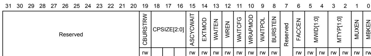
| 31 | 30 | 29 | 28 | 27 | 26 | 25 | 24 | 23 | 22 | 21 | 20 | 19 | 18 | 17 | 16 | 15 | 14 | 13 | 12 | 11 | 10 | 9 | 8 | 7 | 6 | 5 | 4 | 3 | 2 | 1 | 0 |
|---|---|---|---|---|---|---|---|---|---|---|---|---|---|---|---|---|---|---|---|---|---|---|---|---|---|---|---|---|---|---|---|
| Reserved | CBURSTRW | CPSIZE[2:0] | ASYNCWAIT | EXTMOD | WAITEN | WREN | WAITCFG | WRAPMOD | WAITPOL | BURSTEN | Reserved | FACCEN | MWID[1:0] | MTYP[1:0] | MUXEN | MBKEN | |||||||||||||||
| rw | rw | rw | rw | rw | rw | rw | rw | rw | rw | rw | rw | rw | |||||||||||||||||||
Bits 31: 20 Reserved, must be kept at reset value.
Bit 19 CBURSTRW : Write burst enable.
For Cellular RAM (PSRAM) memories, this bit enables the synchronous burst protocol during write operations. The enable bit for synchronous read accesses is the BURSTEN bit in the FSMC_BCRx register.
0: Write operations are always performed in asynchronous mode
1: Write operations are performed in synchronous mode.
Bits 18: 16 CPSIZE[2:0] : CRAM page size.
These are used for Cellular RAM 1.5 which does not allow burst access to cross the address boundaries between pages. When these bits are configured, the FSMC controller splits automatically the burst access when the memory page size is reached (refer to memory datasheet for page size).
000: No burst split when crossing page boundary (default after reset)
001: 128 bytes
010: 256 bytes
011: 512 bytes
100: 1024 bytes
Others: reserved.
Bit 15 ASYNCWAIT : Wait signal during asynchronous transfers
This bit enables/disables the FSMC to use the wait signal even during an asynchronous protocol.
0: NWAIT signal is not taken into account when running an asynchronous protocol (default after reset)
1: NWAIT signal is taken into account when running an asynchronous protocol
Bit 14 EXTMOD: Extended mode enable.This bit enables the FSMC to program the write timings for non-multiplexed asynchronous accesses inside the FSMC_BWTR register, thus resulting in different timings for read and write operations.
0: values inside FSMC_BWTR register are not taken into account (default after reset)
1: values inside FSMC_BWTR register are taken into account
Note: When the extended mode is disabled, the FSMC can operate in Mode1 or Mode2 as follows:
- – Mode 1 is the default mode when the SRAM/PSRAM memory type is selected (MTYP [0:1]=0x0 or 0x01)
- – Mode 2 is the default mode when the NOR memory type is selected (MTYP [0:1]= 0x10).
This bit enables/disables wait-state insertion via the NWAIT signal when accessing the Flash memory in synchronous mode.
0: NWAIT signal is disabled (its level not taken into account, no wait state inserted after the programmed Flash latency period)
1: NWAIT signal is enabled (its level is taken into account after the programmed Flash latency period to insert wait states if asserted) (default after reset)
Bit 12 WREN: Write enable bit.This bit indicates whether write operations are enabled/disabled in the bank by the FSMC:
0: Write operations are disabled in the bank by the FSMC, an AHB error is reported,
1: Write operations are enabled for the bank by the FSMC (default after reset).
Bit 11 WAITCFG: Wait timing configuration.The NWAIT signal indicates whether the data from the memory are valid or if a wait state must be inserted when accessing the Flash memory in synchronous mode. This configuration bit determines if NWAIT is asserted by the memory one clock cycle before the wait state or during the wait state:
0: NWAIT signal is active one data cycle before wait state (default after reset),
1: NWAIT signal is active during wait state (not used for PRAM).
Bit 10 WRAPMOD: Wrapped burst mode support.Defines whether the controller will or not split an AHB burst wrap access into two linear accesses. Valid only when accessing memories in burst mode
0: Direct wrapped burst is not enabled (default after reset),
1: Direct wrapped burst is enabled.
Note: This bit has no effect as the CPU and DMA cannot generate wrapping burst transfers.
Bit 9 WAITPOL: Wait signal polarity bit.Defines the polarity of the wait signal from memory. Valid only when accessing the memory in burst mode:
0: NWAIT active low (default after reset),
1: NWAIT active high.
Bit 8 BURSTEN: Burst enable bit.This bit enables/disables synchronous accesses during read operations. It is valid only for synchronous memories operating in burst mode:
0: Burst mode disabled (default after reset). Read accesses are performed in asynchronous mode.
1: Burst mode enable. Read accesses are performed in synchronous mode.
Bit 7 Reserved, must be kept at reset value.
Bit 6 FACCEN : Flash access enable
Enables NOR Flash memory access operations.
0: Corresponding NOR Flash memory access is disabled
1: Corresponding NOR Flash memory access is enabled (default after reset)
Bits 5:4 MWID[1:0] : Memory databus width.
Defines the external memory device width, valid for all type of memories.
00: 8 bits,
01: 16 bits (default after reset),
10: reserved, do not use,
11: reserved, do not use.
Bits 3:2 MTYP[1:0] : Memory type.
Defines the type of external memory attached to the corresponding memory bank:
00: SRAM (default after reset for Bank 2...4)
01: PSRAM (CRAM)
10: NOR Flash (default after reset for Bank 1)
11: reserved
Bit 1 MUXEN : Address/data multiplexing enable bit.
When this bit is set, the address and data values are multiplexed on the databus, valid only with NOR and PSRAM memories:
0: Address/Data nonmultiplexed
1: Address/Data multiplexed on databus (default after reset)
Bit 0 MBKEN : Memory bank enable bit.
Enables the memory bank. After reset Bank1 is enabled, all others are disabled.
Accessing a disabled bank causes an ERROR on AHB bus.
0: Corresponding memory bank is disabled
1: Corresponding memory bank is enabled
SRAM/NOR-Flash chip-select timing registers 1..4 (FSMC_BTR1..4)
Address offset: \( 0xA000\ 0000 + 0x04 + 8 * (x - 1) \) , \( x = 1..4 \)
Reset value: 0x0FFF FFFF
FSMC_BTRx bits are written by software to add a delay at the end of a read /write transaction. This delay allows matching the minimum time between consecutive transactions ( \( t_{EHEL} \) from NEx high to FSMC_NEx low) and the maximum time required by the memory to free the data bus after a read access ( \( t_{EHQZ} \) ).
This register contains the control information of each memory bank, used for SRAMs, PSRAM and NOR Flash memories. If the EXTMOD bit is set in the FSMC_BCRx register, then this register is partitioned for write and read access, that is, 2 registers are available: one to configure read accesses (this register) and one to configure write accesses (FSMC_BWTRx registers).
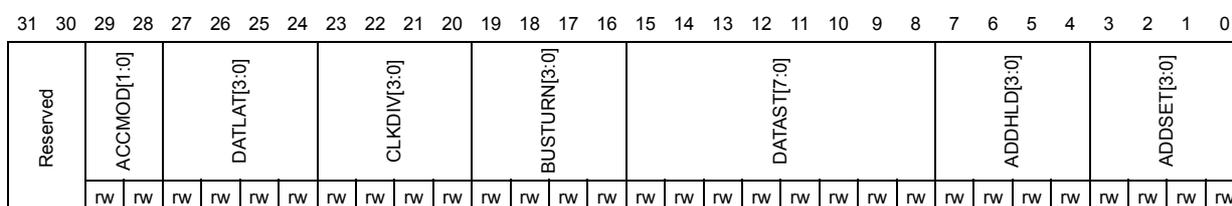
| 31 | 30 | 29 | 28 | 27 | 26 | 25 | 24 | 23 | 22 | 21 | 20 | 19 | 18 | 17 | 16 | 15 | 14 | 13 | 12 | 11 | 10 | 9 | 8 | 7 | 6 | 5 | 4 | 3 | 2 | 1 | 0 |
|---|---|---|---|---|---|---|---|---|---|---|---|---|---|---|---|---|---|---|---|---|---|---|---|---|---|---|---|---|---|---|---|
| Reserved | ACCMOD[1:0] | DATLAT[3:0] | CLKDIV[3:0] | BUSTURN[3:0] | DATAST[7:0] | ADDHLD[3:0] | ADDSET[3:0] | ||||||||||||||||||||||||
| rw | rw | rw | rw | rw | rw | rw | rw | rw | rw | rw | rw | rw | rw | rw | rw | rw | rw | rw | rw | rw | rw | rw | rw | rw | rw | rw | rw | rw | rw | rw | rw |
Bits 31:30 Reserved, must be kept at reset value.
Bits 29:28 ACCMOD[1:0] : Access mode
Specifies the asynchronous access modes as shown in the timing diagrams. These bits are taken into account only when the EXTMOD bit in the FSMC_BCRx register is 1.
- 00: access mode A
- 01: access mode B
- 10: access mode C
- 11: access mode D
Bits 27:24 DATLAT[3:0] : Data latency for synchronous NOR Flash memory (see note below bit description table)
For synchronous NOR Flash memory with burst mode enabled, defines the number of memory clock cycles (+2) to issue to the memory before reading/writing the first data.
This timing parameter is not expressed in HCLK periods, but in FSMC_CLK periods. In case of PSRAM (CRAM), this field must be set to 0. In asynchronous NOR Flash or SRAM or PSRAM, this value is don't care.
- 0000: Data latency of 2 CLK clock cycles for first burst access
- 1111: Data latency of 17 CLK clock cycles for first burst access (default value after reset)
Bits 23:20 CLKDIV[3:0] : Clock divide ratio (for FSMC_CLK signal)
Defines the period of FSMC_CLK clock output signal, expressed in number of HCLK cycles:
- 0000: Reserved
- 0001: FSMC_CLK period = \( 2 \times \) HCLK periods
- 0010: FSMC_CLK period = \( 3 \times \) HCLK periods
- 1111: FSMC_CLK period = \( 16 \times \) HCLK periods (default value after reset)
In asynchronous NOR Flash, SRAM or PSRAM accesses, this value is don't care.
Bits 19:16 BUSTURN[3:0] : Bus turnaround phase durationThese bits are written by software to add a delay at the end of a write-to-read (and read-to write) transaction. The programmed bus turnaround delay is inserted between an asynchronous read (muxed or D mode) or a write transaction and any other asynchronous/synchronous read or write to/from a static bank (for a read operation, the bank can be the same or a different one; for a write operation, the bank can be different except in muxed or D mode).
In some cases, the bus turnaround delay is fixed, whatever the programmed BUSTURN values:
- – No bus turnaround delay is inserted between two consecutive asynchronous write transfers to the same static memory bank except in muxed and D mode.
- – A bus turnaround delay of 1 FSMC clock cycle is inserted between:
- – Two consecutive asynchronous read transfers to the same static memory bank except for muxed and D modes.
- – An asynchronous read to an asynchronous or synchronous write to any static bank or dynamic bank except for muxed and D modes.
- – An asynchronous (modes 1, 2, A, B or C) read and a read operation from another static bank.
- – A bus turnaround delay of 2 FSMC clock cycles is inserted between:
- – Two consecutive synchronous write accesses (in burst or single mode) to the same bank
- – A synchronous write (burst or single) access and an asynchronous write or read transfer to or from static memory bank (the bank can be the same or different in case of a read operation).
- – Two consecutive synchronous read accesses (in burst or single mode) followed by a any synchronous/asynchronous read or write from/to another static memory bank.
- – A bus turnaround delay of 3 FSMC clock cycles is inserted between:
- – Two consecutive synchronous write operations (in burst or single mode) to different static banks.
- – A synchronous write access (in burst or single mode) and a synchronous read access from the same or to a different bank.
0000: BUSTURN phase duration = 1 HCLK clock cycle added
...
1111: BUSTURN phase duration = 16 × HCLK clock cycles (default value after reset)
Bits 15:8 DATAST[7:0] : Data-phase durationThese bits are written by software to define the duration of the data phase (refer to Figure 187 to Figure 199 ), used in asynchronous accesses:
0000 0000: Reserved
0000 0001: DATAST phase duration = 2 × HCLK clock cycles
0000 0010: DATAST phase duration = 3 × HCLK clock cycles
...
1111 1111: DATAST phase duration = 256 × HCLK clock cycles (default value after reset)
For each memory type and access mode data-phase duration, refer to the respective figure ( Figure 187 to Figure 199 ).
Example: Mode1, read access, DATAST=1: Data-phase duration= DATAST+3 = 4 HCLK clock cycles.
Note: In synchronous accesses, this value is don't care.
Bits 7:4 ADDHLD[3:0] : Address-hold phase durationThese bits are written by software to define the duration of the address hold phase (refer to Figure 196 to Figure 199 ), used in mode D and multiplexed accesses:
0000: Reserved
0001: ADDHLD phase duration = 2 × HCLK clock cycle
0010: ADDHLD phase duration = 3 × HCLK clock cycle
...
1111: ADDHLD phase duration = 16 × HCLK clock cycles (default value after reset)
For each access mode address-hold phase duration, refer to the respective figure ( Figure 196 to Figure 199 ).
Example: ModeD, read access, ADDHLD=1: Address-hold phase duration = ADDHLD + 1 = 2 HCLK clock cycles.
Note: In synchronous accesses, this value is not used, the address hold phase is always 1 memory clock period duration.
Bits 3:0 ADDSET[3:0] : Address setup phase durationThese bits are written by software to define the duration of the address setup phase (refer to Figure 187 to Figure 199 ), used in SRAMs, ROMs and asynchronous NOR Flash and PSRAM accesses:
0000: ADDSET phase duration = 1 × HCLK clock cycle
...
1111: ADDSET phase duration = × HCLK clock cycles (default value after reset)
For each access mode address setup phase duration, refer to the respective figure (refer to Figure 187 to Figure 199 ).
Example: Mode2, read access, ADDSET=1: Address setup phase duration = ADDSET + 1 = 2 HCLK clock cycles.
Note: In synchronous NOR Flash and PSRAM accesses, this value is don't care.
Note: PSRAMs (CRAMs) have a variable latency due to internal refresh. Therefore these memories issue the NWAIT signal during the whole latency phase to prolong the latency as needed.
With PSRAMs (CRAMs) the DATLAT field must be set to 0, so that the FSMC exits its latency phase soon and starts sampling NWAIT from memory, then starts to read or write when the memory is ready.
This method can be used also with the latest generation of synchronous Flash memories that issue the NWAIT signal, unlike older Flash memories (check the datasheet of the specific Flash memory being used).
SRAM/NOR-Flash write timing registers 1..4 (FSMC_BWTR1..4)
Address offset: \( 0xA000\ 0000 + 0x104 + 8 * (x - 1) \) , \( x = 1 \dots 4 \)
Reset value: 0x0FFF FFFF
This register contains the control information of each memory bank, used for SRAMs, PSRAMs and NOR Flash memories. This register is active for write asynchronous access only when the EXTMOD bit is set in the FSMC_BCRx register.
| 31 | 30 | 29 | 28 | 27 | 26 | 25 | 24 | 23 | 22 | 21 | 20 | 19 | 18 | 17 | 16 | 15 | 14 | 13 | 12 | 11 | 10 | 9 | 8 | 7 | 6 | 5 | 4 | 3 | 2 | 1 | 0 |
| Res. | ACCMOD[2:0] | Reserved | BUSTURN[3:0] | DATAST[7:0] | ADDHLD[3:0] | ADDSET[3:0] | |||||||||||||||||||||||||
| rw | rw | rw | rw | rw | rw | rw | rw | rw | rw | rw | rw | rw | rw | rw | rw | rw | rw | rw | rw | rw | rw | rw | |||||||||
Bits 31:30 Reserved, must be kept at reset value.
Bits 29:28 ACCMOD[2:0] : Access mode.
Specifies the asynchronous access modes as shown in the next timing diagrams. These bits are taken into account only when the EXTMOD bit in the FSMC_BCRx register is 1.
00: access mode A
01: access mode B
10: access mode C
11: access mode D
Bits 27:20 Reserved, must be kept at reset value.
Bits 19:16 BUSTURN[3:0] : Bus turnaround phase duration
The programmed bus turnaround delay is inserted between a an asynchronous write transfer and any other asynchronous/synchronous read or write transfer to/from a static bank (for a read operation, the bank can be the same or a different one; for a write operation, the bank can be different except in r muxed or D mode).
In some cases, the bus turnaround delay is fixed, whatever the programmed BUSTURN values:
- – No bus turnaround delay is inserted between two consecutive asynchronous write transfers to the same static memory bank except in muxed and D mode.
- – A bus turnaround delay of 2 FSMC clock cycles is inserted between:
- – Two consecutive synchronous write accesses (in burst or single mode) to the same bank.
- – A synchronous write transfer (in burst or single mode) and an asynchronous write or read transfer to/from static a memory bank.
- – A bus turnaround delay of 3 FSMC clock cycles is inserted between:
- – Two consecutive synchronous write accesses (in burst or single mode) to different static banks.
- – A synchronous write transfer (in burst or single mode) and a synchronous read from the same or from a different bank.
0000: BUSTURN phase duration = 1 HCLK clock cycle added
...
1111: BUSTURN phase duration = 16 HCLK clock cycles added (default value after reset)
Bits 15:8 DATAST[7:0] : Data-phase duration.
These bits are written by software to define the duration of the data phase (refer to Figure 187 to Figure 199 ), used in asynchronous SRAM, PSRAM and NOR Flash memory accesses:
0000 0000: Reserved
0000 0001: DATAST phase duration = 2 × HCLK clock cycles
0000 0010: DATAST phase duration = 3 × HCLK clock cycles
...
1111 1111: DATAST phase duration = 16 × HCLK clock cycles (default value after reset)
Note: In synchronous accesses, this value is don't care.
Bits 7:4 ADDHLD[3:0] : Address-hold phase duration.
These bits are written by software to define the duration of the address hold phase (refer to Figure 196 to Figure 199 ), used in asynchronous multiplexed accesses:
0000: Reserved
0001: ADDHLD phase duration = 2 × HCLK clock cycle
0010: ADDHLD phase duration = 3 × HCLK clock cycle
...
1111: ADDHLD phase duration = 16 × HCLK clock cycles (default value after reset)
Note: In synchronous NOR Flash accesses, this value is not used, the address hold phase is always 1 Flash clock period duration.
Bits 3:0 ADDSET[3:0] : Address setup phase duration.
These bits are written by software to define the duration of the address setup phase in HCLK cycles (refer to Figure 196 to Figure 199 ), used in asynchronous accessed:
0000: ADDSET phase duration = 1 × HCLK clock cycle
...
1111: ADDSET phase duration = 16 × HCLK clock cycles (default value after reset)
Note: In synchronous NOR Flash and PSRAM accesses, this value is don't care.
21.6 NAND Flash/PC Card controller
The FSMC generates the appropriate signal timings to drive the following types of device:
- • NAND Flash
- – 8-bit
- – 16-bit
- • 16-bit PC Card compatible devices
The NAND/PC Card controller can control three external banks. Bank 2 and bank 3 support NAND Flash devices. Bank 4 supports PC Card devices.
Each bank is configured by means of dedicated registers ( Section 21.6.8 ). The programmable memory parameters include access timings (shown in Table 129 ) and ECC configuration.
Table 129. Programmable NAND/PC Card access parameters| Parameter | Function | Access mode | Unit | Min. | Max. |
|---|---|---|---|---|---|
| Memory setup time | Number of clock cycles (HCLK) to set up the address before the command assertion | Read/Write | AHB clock cycle (HCLK) | 1 | 255 |
| Memory wait | Minimum duration (HCLK clock cycles) of the command assertion | Read/Write | AHB clock cycle (HCLK) | 2 | 256 |
| Memory hold | Number of clock cycles (HCLK) to hold the address (and the data in case of a write access) after the command de-assertion | Read/Write | AHB clock cycle (HCLK) | 1 | 254 |
| Memory databus high-Z | Number of clock cycles (HCLK) during which the databus is kept in high-Z state after the start of a write access | Write | AHB clock cycle (HCLK) | 0 | 255 |
21.6.1 External memory interface signals
The following tables list the signals that are typically used to interface NAND Flash and PC Card.
Caution: When using a PC Card or a CompactFlash in I/O mode, the NIOS16 input pin must remain at ground level during the whole operation, otherwise the FSMC may not operate properly. This means that the NIOS16 input pin must not be connected to the card, but directly to ground (only 16-bit accesses are allowed).
Note: Prefix “N” specifies the associated signal as active low.
8-bit NAND Flash
Table 130. 8-bit NAND Flash| FSMC signal name | I/O | Function |
|---|---|---|
| A[17] | O | NAND Flash address latch enable (ALE) signal |
| A[16] | O | NAND Flash command latch enable (CLE) signal |
| D[7:0] | I/O | 8-bit multiplexed, bidirectional address/data bus |
| NCE[x] | O | Chip select, x = 2, 3 |
| NOE(= NRE) | O | Output enable (memory signal name: read enable, NRE) |
| NWE | O | Write enable |
| NWAIT/INT[3:2] | I | NAND Flash ready/busy input signal to the FSMC |
There is no theoretical capacity limitation as the FSMC can manage as many address cycles as needed.
16-bit NAND Flash
Table 131. 16-bit NAND Flash
| FSMC signal name | I/O | Function |
|---|---|---|
| A[17] | O | NAND Flash address latch enable (ALE) signal |
| A[16] | O | NAND Flash command latch enable (CLE) signal |
| D[15:0] | I/O | 16-bit multiplexed, bidirectional address/data bus |
| NCE[x] | O | Chip select, x = 2, 3 |
| NOE(= NRE) | O | Output enable (memory signal name: read enable, NRE) |
| NWE | O | Write enable |
| NWAIT/INT[3:2] | I | NAND Flash ready/busy input signal to the FSMC |
There is no theoretical capacity limitation as the FSMC can manage as many address cycles as needed.
16-bit PC Card
Table 132. 16-bit PC Card
| FSMC signal name | I/O | Function |
|---|---|---|
| A[10:0] | O | Address bus |
| NIOS16 | I | Data transfer in I/O space. It must be shorted to GND (16-bit transfer only) |
| NIORD | O | Output enable for I/O space |
| NIOWR | O | Write enable for I/O space |
| NREG | O | Register signal indicating if access is in Common or Attribute space |
| D[15:0] | I/O | Bidirectional databus |
| NCE4_1 | O | Chip select 1 |
| NCE4_2 | O | Chip select 2 (indicates if access is 16-bit or 8-bit) |
| NOE | O | Output enable in Common and in Attribute space |
| NWE | O | Write enable in Common and in Attribute space |
| NWAIT | I | PC Card wait input signal to the FSMC (memory signal name IORDY) |
| INTR | I | PC Card interrupt to the FSMC (only for PC Cards that can generate an interrupt) |
| CD | I | PC Card presence detection. Active high. If an access is performed to the PC Card banks while CD is low, an AHB error is generated. Refer to Section 21.3: AHB interface |
21.6.2 NAND Flash / PC Card supported memories and transactions
Table 133 below shows the supported devices, access modes and transactions. Transactions not allowed (or not supported) by the NAND Flash / PC Card controller appear in gray.
Table 133. Supported memories and transactions
| Device | Mode | R/W | AHB data size | Memory data size | Allowed/not allowed | Comments |
|---|---|---|---|---|---|---|
| NAND 8-bit | Asynchronous | R | 8 | 8 | Y | |
| Asynchronous | W | 8 | 8 | Y | ||
| Asynchronous | R | 16 | 8 | Y | Split into 2 FSMC accesses | |
| Asynchronous | W | 16 | 8 | Y | Split into 2 FSMC accesses | |
| Asynchronous | R | 32 | 8 | Y | Split into 4 FSMC accesses | |
| Asynchronous | W | 32 | 8 | Y | Split into 4 FSMC accesses | |
| NAND 16-bit | Asynchronous | R | 8 | 16 | Y | |
| Asynchronous | W | 8 | 16 | N | ||
| Asynchronous | R | 16 | 16 | Y | ||
| Asynchronous | W | 16 | 16 | Y | ||
| Asynchronous | R | 32 | 16 | Y | Split into 2 FSMC accesses | |
| Asynchronous | W | 32 | 16 | Y | Split into 2 FSMC accesses |
21.6.3 Timing diagrams for NAND and PC Card
Each PC Card/CompactFlash and NAND Flash memory bank is managed through a set of registers:
- • Control register: FSMC_PCRx
- • Interrupt status register: FSMC_SRx
- • ECC register: FSMC_ECCRx
- • Timing register for Common memory space: FSMC_PMEMx
- • Timing register for Attribute memory space: FSMC_PATTx
- • Timing register for I/O space: FSMC_PIOx
Each timing configuration register contains three parameters used to define number of HCLK cycles for the three phases of any PC Card/CompactFlash or NAND Flash access, plus one parameter that defines the timing for starting driving the databus in the case of a write. Figure 205 shows the timing parameter definitions for common memory accesses, knowing that Attribute and I/O (only for PC Card) memory space access timings are similar.
Figure 205. NAND/PC Card controller timing for common memory access
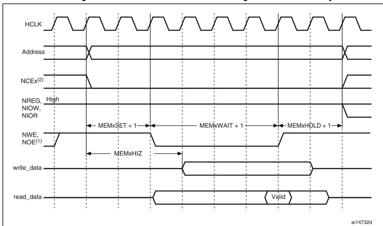
The timing diagram shows the relationship between various signals during a memory access. HCLK is a periodic clock signal. Address is stable during the access. NCEX(2) goes low to initiate the access. NREG, NIOW, and NIOR are shown as high. NWE and NOE(1) are active-low signals; NWE is low during the write phase, and NOE(1) is high. write_data is driven by the CPU during the write phase. read_data is driven by the memory device during the read phase and is marked as 'Valid' for a specific duration. Timing parameters are defined as follows: MEMxSET + 1 is the time from Address/NCEX(2) setup to the first clock edge; MEMxWAIT + 1 is the duration of the access; MEMxHOLD + 1 is the time from the last clock edge to Address/NCEX(2) hold; MEMxHIZ is the time from the start of the access to the read_data bus becoming high-impedance.
- 1. NOE remains high (inactive) during write access. NWE remains high (inactive) during read access.
- 2. NCEX goes low as soon as NAND access is requested and remains low until a different memory bank is accessed.
21.6.4 NAND Flash operations
The command latch enable (CLE) and address latch enable (ALE) signals of the NAND Flash device are driven by some address signals of the FSMC controller. This means that to send a command or an address to the NAND Flash memory, the CPU has to perform a write to a certain address in its memory space.
A typical page read operation from the NAND Flash device is as follows:
- 1. Program and enable the corresponding memory bank by configuring the FSMC_PCRx and FSMC_PMEMx (and for some devices, FSMC_PATTx, see Section 21.6.5 ) registers according to the characteristics of the NAND Flash (PWID bits for the databus width of the NAND Flash, PTYP = 1, PWAITEN = 0 or 1 as needed, see Common memory space timing register 2..4 (FSMC_PMEM2..4) for timing configuration).
- 2. The CPU performs a byte write in the common memory space, with data byte equal to one Flash command byte (for example 0x00 for Samsung NAND Flash devices). The CLE input of the NAND Flash is active during the write strobe (low pulse on NWE), thus the written byte is interpreted as a command by the NAND Flash. Once the command is latched by the NAND Flash device, it does not need to be written for the following page read operations.
- 3. The CPU can send the start address (STARTAD) for a read operation by writing the required bytes (for example four bytes or three for smaller capacity devices), STARTAD[7:0], STARTAD[15:8], STARTAD[23:16] and finally STARTAD[25:24] for 64 Mb x 8 bit NAND Flash) in the common memory or attribute space. The ALE input of the NAND Flash device is active during the write strobe (low pulse on NWE), thus the written bytes are interpreted as the start address for read operations. Using the
attribute memory space makes it possible to use a different timing configuration of the FSMC, which can be used to implement the prewait functionality needed by some NAND Flash memories (see details in Section 21.6.5 ).
- 4. The controller waits for the NAND Flash to be ready (R/NB signal high) to become active, before starting a new access (to same or another memory bank). While waiting, the controller maintains the NCE signal active (low).
- 5. The CPU can then perform byte read operations in the common memory space to read the NAND Flash page (data field + Spare field) byte by byte.
- 6. The next NAND Flash page can be read without any CPU command or address write operation, in three different ways:
- – by simply performing the operation described in step 5
- – a new random address can be accessed by restarting the operation at step 3
- – a new command can be sent to the NAND Flash device by restarting at step 2
21.6.5 NAND Flash prewait functionality
Some NAND Flash devices require that, after writing the last part of the address, the controller wait for the R/NB signal to go low as shown in Figure 206 .
Figure 206. Access to non 'CE don't care' NAND-Flash
![Timing diagram for Figure 206 showing the sequence of signals for a NAND Flash write access. The signals shown are NCE, CLE, ALE, NWE, NOE, I/O[7:0], and R/NB. The sequence is divided into five steps: (1) CPU wrote byte 0x00 at address 0x7001 0000; (2) CPU wrote byte A7-A0 at address 0x7002 0000; (3) CPU wrote byte A15-A8 at address 0x7002 0000; (4) CPU wrote byte A23-A16 at address 0x7002 0000; (5) CPU wrote byte A25-A24 at address 0x7802 0000. The diagram shows the NCE signal staying low throughout the access, the CLE signal going high for the command, the ALE signal going high for the address, and the NWE signal going low for the write. The I/O[7:0] bus shows the data and address bytes. The R/NB signal is shown going low at the end of step 5, indicating the device is busy. Timing parameters tR and tWB are indicated.](/RM0008-STM32F101-102-103-105-107/296ce62e83a65d9de9c5c6f361cd6d18_img.jpg)
- 1. CPU wrote byte 0x00 at address 0x7001 0000.
- 2. CPU wrote byte A7-A0 at address 0x7002 0000.
- 3. CPU wrote byte A15-A8 at address 0x7002 0000.
- 4. CPU wrote byte A23-A16 at address 0x7002 0000.
- 5. CPU wrote byte A25-A24 at address 0x7802 0000: FSMC performs a write access using FSMC_PATT2 timing definition, where \( ATTHOLD \geq 7 \) (providing that \( (7+1) \times HCLK = 112 \text{ ns} > t_{WB} \text{ max} \) ). This guarantees that NCE remains low until R/NB goes low and high again (only requested for NAND Flash memories where NCE is not don't care).
When this functionality is needed, it can be guaranteed by programming the MEMHOLD value to meet the \( t_{WB} \) timing. However CPU read accesses to the NAND Flash memory have a hold delay of \( (\text{MEMHOLD} + 2) \times \text{HCLK} \) cycles, while CPU write accesses have a hold delay of \( (\text{MEMHOLD}) \times \text{HCLK} \) cycles.
To overcome this timing constraint, the attribute memory space can be used by programming its timing register with an ATTHOLD value that meets the \( t_{WB} \) timing, and leaving the MEMHOLD value at its minimum. Then, the CPU must use the common memory space for all NAND Flash read and write accesses, except when writing the last address byte to the NAND Flash device, where the CPU must write to the attribute memory space.
21.6.6 Computation of the error correction code (ECC) in NAND Flash memory
The FSMC PC-Card controller includes two error correction code computation hardware blocks, one per memory bank. They are used to reduce the host CPU workload when processing the error correction code by software in the system.
These two registers are identical and associated with bank 2 and bank 3, respectively. As a consequence, no hardware ECC computation is available for memories connected to bank 4.
The error correction code (ECC) algorithm implemented in the FSMC can perform 1-bit error correction and 2-bit error detection per 256, 512, 1 024, 2 048, 4 096 or 8 192 bytes read from or written to NAND Flash memory. It is based on the Hamming coding algorithm and consists in calculating the row and column parity.
The ECC modules monitor the NAND Flash databus and read/write signals (NCE and NWE) each time the NAND Flash memory bank is active.
The functional operations are:
- • When access to NAND Flash is made to bank 2 or bank 3, the data present on the D[15:0] bus is latched and used for ECC computation.
- • When access to NAND Flash occurs at any other address, the ECC logic is idle, and does not perform any operation. Thus, write operations for defining commands or addresses to NAND Flash are not taken into account for ECC computation.
Once the desired number of bytes has been read from/written to the NAND Flash by the host CPU, the FSMC_ECCR2/3 registers must be read in order to retrieve the computed value. Once read, they should be cleared by resetting the ECCEN bit to zero. To compute a new data block, the ECCEN bit must be set to one in the FSMC_PCR2/3 registers.
To perform an ECC computation:
- 1. Enable the ECCEN bit in the FSMC_PCR2/3 register.
- 2. Write data to the NAND Flash memory page. While the NAND page is written, the ECC block computes the ECC value.
- 3. Read the ECC value available in the FSMC_ECCR2/3 register and store it in a variable.
- 4. Clear the ECCEN bit and then enable it in the FSMC_PCR2/3 register before reading back the written data from the NAND page. While the NAND page is read, the ECC block computes the ECC value.
- 5. Read the new ECC value available in the FSMC_ECCR2/3 register.
- 6. If the two ECC values are the same, no correction is required, otherwise there is an ECC error and the software correction routine returns information on whether the error can be corrected or not.
21.6.7 PC Card/CompactFlash operations
Address spaces and memory accesses
The FSMC supports Compact Flash storage or PC Cards in Memory Mode and I/O Mode (True IDE mode is not supported).
The Compact Flash storage and PC Cards are made of 3 memory spaces:
- • Common Memory Space
- • Attribute Space
- • I/O Memory Space
The nCE2 and nCE1 pins (FSMC_NCE4_2 and FSMC_NCE4_1 respectively) select the card and indicate whether a byte or a word operation is being performed: nCE2 accesses the odd byte on D15-8 and nCE1 accesses the even byte on D7-0 if A0=0 or the odd byte on D7-0 if A0=1. The full word is accessed on D15-0 if both nCE2 and nCE1 are low.
The memory space is selected by asserting low nOE for read accesses or nWE for write accesses, combined with the low assertion of nCE2/nCE1 and nREG.
- • If pin nREG=1 during the memory access, the common memory space is selected
- • If pin nREG=0 during the memory access, the attribute memory space is selected
The I/O Space is selected by asserting low nIORD for read accesses or nIOWR for write accesses [instead of nOE/nWE for memory Space], combined with nCE2/nCE1. Note that nREG must also be asserted low during accesses to I/O Space.
Three type of accesses are allowed for a 16-bit PC Card:
- • Accesses to Common Memory Space for data storage can be either 8-bit accesses at even addresses or 16 bit AHB accesses.
Note that 8-bit accesses at odd addresses are not supported and will not lead to the low assertion of nCE2. A 32-bit AHB request is translated into two 16-bit memory accesses.
- • Accesses to Attribute Memory Space where the PC Card stores configuration information are limited to 8-bit AHB accesses at even addresses.
Note that a 16-bit AHB access will be converted into a single 8-bit memory transfer: nCE1 will be asserted low, nCE2 will be asserted high and only the even Byte on D7-D0 will be valid. Instead a 32-bit AHB access will be converted into two 8-bit memory
transfers at even addresses: nCE1 will be asserted low, NCE2 will be asserted high and only the even bytes will be valid.
- • Accesses to I/O Space can be performed either through AHB 8-bit or 16-bit accesses.
Table 134. 16-bit PC-Card signals and access type
| nCE2 | nCE1 | nREG | nOE/nWE | nIORD /nIOWR | A10 | A9 | A7-1 | A0 | Space | Access Type | Allowed/not Allowed |
|---|---|---|---|---|---|---|---|---|---|---|---|
| 1 | 0 | 1 | 0 | 1 | X | X | X-X | X | Common Memory Space | Read/Write byte on D7-D0 | YES |
| 0 | 1 | 1 | 0 | 1 | X | X | X-X | X | Read/Write byte on D15-D8 | Not supported | |
| 0 | 0 | 1 | 0 | 1 | X | X | X-X | 0 | Read/Write word on D15-D0 | YES | |
| X | 0 | 0 | 0 | 1 | 0 | 1 | X-X | 0 | Attribute Space | Read or Write Configuration registers | YES |
| X | 0 | 0 | 0 | 1 | 0 | 0 | X-X | 0 | Read or Write CIS (Card Information Structure) | YES | |
| 1 | 0 | 0 | 0 | 1 | X | X | X-X | 1 | Attribute Space | Invalid Read or Write (odd address) | YES |
| 0 | 1 | 0 | 0 | 1 | X | X | X-X | x | Invalid Read or Write (odd address) | YES | |
| 1 | 0 | 0 | 1 | 0 | X | X | X-X | 0 | I/O space | Read Even Byte on D7-0 | YES |
| 1 | 0 | 0 | 1 | 0 | X | X | X-X | 1 | Read Odd Byte on D7-0 | YES | |
| 1 | 0 | 0 | 1 | 0 | X | X | X-X | 0 | Write Even Byte on D7-0 | YES | |
| 1 | 0 | 0 | 1 | 0 | X | X | X-X | 1 | Write Odd Byte on D7-0 | YES | |
| 0 | 0 | 0 | 1 | 0 | X | X | X-X | 0 | Read Word on D15-0 | YES | |
| 0 | 0 | 0 | 1 | 0 | X | X | X-X | 0 | Write word on D15-0 | YES | |
| 0 | 1 | 0 | 1 | 0 | X | X | X-X | X | Read Odd Byte on D15-8 | Not supported | |
| 0 | 1 | 0 | 1 | 0 | X | X | X-X | X | Write Odd Byte on D15-8 | Not supported | |
| 0 | 1 | 0 | 1 | 0 | X | X | X-X | X |
The FSMC Bank 4 gives access to those 3 memory spaces as described in Section 21.4.2: NAND/PC Card address mapping and Table 102: Memory mapping and timing registers .
Wait Feature
The CompactFlash Storage or PC Card may request the FSMC to extend the length of the access phase programmed by MEMWAITx/ATTWAITx/IOWAITx bits, asserting the nWAIT signal after nOE/nWE or nIORD/nIOWR activation if the wait feature is enabled through the PWAITEN bit in the FSMC_PCRx register. In order to detect the nWAIT assertion correctly, the MEMWAITx/ATTWAITx/IOWAITx bits must be programmed as follows:
xxWAITx >= 4 + max_wait_assertion_time/HCLK
Where max_wait_assertion_time is the maximum time taken by NWAIT to go low once nOE/nWE or nIORD/nIOWR is low.
After the de-assertion of nWAIT, the FSMC extends the WAIT phase for 4 HCLK clock cycles.
21.6.8 NAND Flash/PC Card control registers
The NAND Flash/PC Card control registers have to be accessed by words (32 bits).
PC Card/NAND Flash control registers 2..4 (FSMC_PCR2..4)
Address offset: 0xA0000000 + 0x40 + 0x20 * (x - 1), x = 2..4
Reset value: 0x0000 0018
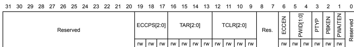
| 31 | 30 | 29 | 28 | 27 | 26 | 25 | 24 | 23 | 22 | 21 | 20 | 19 | 18 | 17 | 16 | 15 | 14 | 13 | 12 | 11 | 10 | 9 | 8 | 7 | 6 | 5 | 4 | 3 | 2 | 1 | 0 |
|---|---|---|---|---|---|---|---|---|---|---|---|---|---|---|---|---|---|---|---|---|---|---|---|---|---|---|---|---|---|---|---|
| Reserved | ECCPS[2:0] | TAR[2:0] | TCLR[2:0] | Res. | ECCEN | PWID[1:0] | PTYP | PBKEN | PWAITEN | Reserved | |||||||||||||||||||||
| rw | rw | rw | rw | rw | rw | rw | rw | rw | rw | rw | rw | ||||||||||||||||||||
Bits 31:20 Reserved, must be kept at reset value.
Bits 19:17 ECCPS[2:0] : ECC page size.
Defines the page size for the extended ECC:
- 000: 256 bytes
- 001: 512 bytes
- 010: 1024 bytes
- 011: 2048 bytes
- 100: 4096 bytes
- 101: 8192 bytes
Bits 16:13 TAR[2:0] : ALE to RE delay.
Sets time from ALE low to RE low in number of AHB clock cycles (HCLK).
Time is: \( t\_ar = (TAR + SET + 4) \times THCLK \) where THCLK is the HCLK clock period
- 0000: 1 HCLK cycle (default)
- 1111: 16 HCLK cycles
Note: SET is MEMSET or ATTSET according to the addressed space.
Bits 12:9 TCLR[2:0] : CLE to RE delay.
Sets time from CLE low to RE low in number of AHB clock cycles (HCLK).
Time is: \( t\_clr = (TCLR + SET + 4) \times THCLK \) where THCLK is the HCLK clock period
- 0000: 1 HCLK cycle (default)
- 1111: 16 HCLK cycles
Note: SET is MEMSET or ATTSET according to the addressed space.
Bits 8:7 Reserved, must be kept at reset value.
Bit 6 ECCEN : ECC computation logic enable bit
- 0: ECC logic is disabled and reset (default after reset),
- 1: ECC logic is enabled.
Bits 5:4 PWID[1:0] : Databus width.
- Defines the external memory device width.
- 00: 8 bits
- 01: 16 bits (default after reset). This value is mandatory for PC Cards.
- 10: reserved, do not use
- 11: reserved, do not use
Bit 3 PTYP : Memory type.
- Defines the type of device attached to the corresponding memory bank:
- 0: PC Card, CompactFlash, CF+ or PCMCIA
- 1: NAND Flash (default after reset)
Bit 2 PBKEN : PC Card/NAND Flash memory bank enable bit.
- Enables the memory bank. Accessing a disabled memory bank causes an ERROR on AHB bus
- 0: Corresponding memory bank is disabled (default after reset)
- 1: Corresponding memory bank is enabled
Bit 1 PWAITEN : Wait feature enable bit.
- Enables the Wait feature for the PC Card/NAND Flash memory bank:
- 0: disabled
- 1: enabled
Note: For a PC Card, when the wait feature is enabled, the MEMWAITx/ATTWAITx/IOWAITx bits must be programmed to a value as follows:
\( xxWAITx \geq 4 + max\_wait\_assertion\_time/HCLK \)
Where max_wait_assertion_time is the maximum time taken by NWAIT to go low once nOE/nWE or nIORD/nIOWR is low.
Bit 0 Reserved, must be kept at reset value.
FIFO status and interrupt register 2..4 (FSMC_SR2..4)
Address offset: 0xA000 0000 + 0x44 + 0x20 * (x-1), x = 2..4
Reset value: 0x0000 0040
This register contains information about FIFO status and interrupt. The FSMC has a FIFO that is used when writing to memories to store up to 16 words of data from the AHB. This is used to quickly write to the AHB and free it for transactions to peripherals other than the FSMC, while the FSMC is draining its FIFO into the memory. This register has one of its bits that indicates the status of the FIFO, for ECC purposes.
The ECC is calculated while the data are written to the memory, so in order to read the correct ECC the software must wait until the FIFO is empty.
| 31 | 30 | 29 | 28 | 27 | 26 | 25 | 24 | 23 | 22 | 21 | 20 | 19 | 18 | 17 | 16 | 15 | 14 | 13 | 12 | 11 | 10 | 9 | 8 | 7 | 6 | 5 | 4 | 3 | 2 | 1 | 0 |
|---|---|---|---|---|---|---|---|---|---|---|---|---|---|---|---|---|---|---|---|---|---|---|---|---|---|---|---|---|---|---|---|
| Reserved | FEMPT | IFEN | ILEN | IREN | IFS | ILS | IRS | ||||||||||||||||||||||||
| r | rw | rw | rw | rw | rw | rw | |||||||||||||||||||||||||
Bits 31:7 Reserved, must be kept at reset value.
Bit 6 FEMPT : FIFO empty.
Read-only bit that provides the status of the FIFO
0: FIFO not empty
1: FIFO empty
Bit 5 IFEN : Interrupt falling edge detection enable bit
0: Interrupt falling edge detection request disabled
1: Interrupt falling edge detection request enabled
Bit 4 ILEN : Interrupt high-level detection enable bit
0: Interrupt high-level detection request disabled
1: Interrupt high-level detection request enabled
Bit 3 IREN : Interrupt rising edge detection enable bit
0: Interrupt rising edge detection request disabled
1: Interrupt rising edge detection request enabled
Bit 2 IFS : Interrupt falling edge status
The flag is set by hardware and reset by software.
0: No interrupt falling edge occurred
1: Interrupt falling edge occurred
Note: This bit is set by programming it to 1 by software.
Bit 1 ILS : Interrupt high-level status
The flag is set by hardware and reset by software.
0: No Interrupt high-level occurred
1: Interrupt high-level occurred
Bit 0 IRS : Interrupt rising edge status
The flag is set by hardware and reset by software.
0: No interrupt rising edge occurred
1: Interrupt rising edge occurred
Note: This bit is set by programming it to 1 by software.
Common memory space timing register 2..4 (FSMC_PMEM2..4)
Address offset: Address: \( 0xA000\ 0000 + 0x48 + 0x20 * (x - 1) \) , \( x = 2..4 \)
Reset value: 0xFCFC FCFC
Each FSMC_PMEMx ( \( x = 2..4 \) ) read/write register contains the timing information for PC Card or NAND Flash memory bank x, used for access to the common memory space of the 16-bit PC Card/CompactFlash, or to access the NAND Flash for command, address write access and data read/write access.
| 31 | 30 | 29 | 28 | 27 | 26 | 25 | 24 | 23 | 22 | 21 | 20 | 19 | 18 | 17 | 16 | 15 | 14 | 13 | 12 | 11 | 10 | 9 | 8 | 7 | 6 | 5 | 4 | 3 | 2 | 1 | 0 |
|---|---|---|---|---|---|---|---|---|---|---|---|---|---|---|---|---|---|---|---|---|---|---|---|---|---|---|---|---|---|---|---|
| MEMHIZ[7:0] | MEMHOLD[7:0] | MEMWAIT[7:0] | MEMSET[7:0] | ||||||||||||||||||||||||||||
| rw | rw | rw | rw | rw | rw | rw | rw | rw | rw | rw | rw | rw | rw | rw | rw | rw | rw | rw | rw | rw | rw | rw | rw | rw | rw | rw | rw | rw | rw | rw | rw |
Bits 31:24 MEMHIZx[7:0] : Common memory x databus HiZ time
Defines the number of HCLK (+1 only for NAND) clock cycles during which the databus is kept in HiZ after the start of a PC Card/NAND Flash write access to common memory space on socket x. Only valid for write transaction:
0000 0000: 1 HCLK cycle
1111 1110: 255 HCLK cycles
1111 1111: Reserved
Bits 23:16 MEMHOLDx[7:0] : Common memory x hold time
For NAND Flash read accesses to the common memory space, these bits define the number of (HCLK+2) clock cycles during which the address is held after the command is deasserted (NWE, NOE).
For NAND Flash write accesses to the common memory space, these bits define the number of HCLK clock cycles during which the data are held after the command is deasserted (NWE, NOE).
0000 0000: Reserved
0000 0001: 1 HCLK cycle for write accesses, 3 HCLK cycles for read accesses
1111 1110: 254 HCLK cycle for write accesses, 256 HCLK cycles for read accesses
1111 1111: Reserved
Bits 15:8 MEMWAITx[7:0] : Common memory x wait time
Defines the minimum number of HCLK (+1) clock cycles to assert the command (NWE, NOE), for PC Card/NAND Flash read or write access to common memory space on socket x. The duration for command assertion is extended if the wait signal (NWAIT) is active (low) at the end of the programmed value of HCLK:
0000 0000: Reserved
0000 0001: 2 HCLK cycles (+ wait cycle introduced by deasserting NWAIT)
1111 1110: 255 HCLK cycles (+ wait cycle introduced by deasserting NWAIT)
1111 1111: Reserved.
Bits 7:0 MEMSETx[7:0] : Common memory x setup time
Defines the number of HCLK (+1 for PC Card, +2 for NAND) clock cycles to set up the address before the command assertion (NWE, NOE), for PC Card/NAND Flash read or write access to common memory space on socket x:
0000 0000: 1 HCLK cycle
1111 1110: 255 HCLK cycles
1111 1111: Reserved
Attribute memory space timing registers 2..4 (FSMC_PATT2..4)
Address offset: 0xA000 0000 + 0x4C + 0x20 * (x - 1), x = 2..4
Reset value: 0xFCFC FCFC
Each FSMC_PATTx (x = 2..4) read/write register contains the timing information for PC Card/CompactFlash or NAND Flash memory bank x. It is used for 8-bit accesses to the attribute memory space of the PC Card/CompactFlash or to access the NAND Flash for the last address write access if the timing must differ from that of previous accesses (for Ready/Busy management, refer to Section 21.6.5: NAND Flash prewait functionality ).
| 31 | 30 | 29 | 28 | 27 | 26 | 25 | 24 | 23 | 22 | 21 | 20 | 19 | 18 | 17 | 16 | 15 | 14 | 13 | 12 | 11 | 10 | 9 | 8 | 7 | 6 | 5 | 4 | 3 | 2 | 1 | 0 |
|---|---|---|---|---|---|---|---|---|---|---|---|---|---|---|---|---|---|---|---|---|---|---|---|---|---|---|---|---|---|---|---|
| ATTHIZ[7:0] | ATTHOLD[7:0] | ATTWAIT[7:0] | ATTSET[7:0] | ||||||||||||||||||||||||||||
| rw | rw | rw | rw | rw | rw | rw | rw | rw | rw | rw | rw | rw | rw | rw | rw | rw | rw | rw | rw | rw | rw | rw | rw | rw | rw | rw | rw | rw | rw | rw | rw |
Bits 31:24 ATTHIZ[7:0] : Attribute memory x databus HiZ time
Defines the number of HCLK clock cycles during which the databus is kept in HiZ after the start of a PC CARD/NAND Flash write access to attribute memory space on socket x. Only valid for write transaction:
0000 0000: 0 HCLK cycle
1111 1110: 255 HCLK cycles
1111 1111: Reserved.
Bits 23:16 ATTHOLD[7:0] : Attribute memory x hold time
For PC Card/NAND Flash read accesses to attribute memory space on socket x, these bits define the number of HCLK clock cycles \( (HCLK + 2) \) clock cycles during which the address is held after the command is deasserted (NWE, NOE).
For PC Card/NAND Flash write accesses to attribute memory space on socket x, these bits define the number of HCLK clock cycles during which the data are held after the command is deasserted (NWE, NOE).
0000 0000: reserved
0000 0001: 1 HCLK cycle for write access, 3 HCLK cycles for read accesses
1111 1110: 254 HCLK cycle for write access, 256 HCLK cycles for read accesses
1111 1111: Reserved
Bits 15:8 ATTWAIT[7:0] : Attribute memory x wait time
Defines the minimum number of HCLK \( (+1) \) clock cycles to assert the command (NWE, NOE), for PC Card/NAND Flash read or write access to attribute memory space on socket x. The duration for command assertion is extended if the wait signal (NWAIT) is active (low) at the end of the programmed value of HCLK:
0000 0000: Reserved
0000 0001: 2 HCLK cycles (+ wait cycle introduced by deassertion of NWAIT)
1111 1110: 255 HCLK cycles (+ wait cycle introduced by deasserting NWAIT)
1111 1111: Reserved.
Bits 7:0 ATTSET[7:0] : Attribute memory x setup time
Defines the number of HCLK \( (+1) \) clock cycles to set up address before the command assertion (NWE, NOE), for PC CARD/NAND Flash read or write access to attribute memory space on socket x:
0000 0000: 1 HCLK cycle
1111 1110: 255 HCLK cycles
1111 1111: Reserved.
I/O space timing register 4 (FSMC_PIO4)
Address offset: 0xA000 0000 + 0xB0
Reset value: 0xFCFCFCFC
The FSMC_PIO4 read/write registers contain the timing information used to gain access to the I/O space of the 16-bit PC Card/CompactFlash.
| 31 | 30 | 29 | 28 | 27 | 26 | 25 | 24 | 23 | 22 | 21 | 20 | 19 | 18 | 17 | 16 | 15 | 14 | 13 | 12 | 11 | 10 | 9 | 8 | 7 | 6 | 5 | 4 | 3 | 2 | 1 | 0 |
|---|---|---|---|---|---|---|---|---|---|---|---|---|---|---|---|---|---|---|---|---|---|---|---|---|---|---|---|---|---|---|---|
| IOHIZ[7:0] | IOHOLD[7:0] | IOWAIT[7:0] | IOSET[7:0] | ||||||||||||||||||||||||||||
| rw | rw | rw | rw | rw | rw | rw | rw | rw | rw | rw | rw | rw | rw | rw | rw | rw | rw | rw | rw | rw | rw | rw | rw | rw | rw | rw | rw | rw | rw | rw | rw |
Bits 31:24 IOHIZ[7:0] : I/O x databus HiZ time
Defines the number of HCLK clock cycles during which the databus is kept in HiZ after the start of a PC Card write access to I/O space on socket x. Only valid for write transaction:
0000 0000: 0 HCLK cycle
1111 1111: 255 HCLK cycles (default value after reset)
Bits 23:16 IOHOLD[7:0] : I/O x hold time
Defines the number of HCLK clock cycles to hold address (and data for write access) after the command deassertion (NWE, NOE), for PC Card read or write access to I/O space on socket x:
0000 0000: reserved
0000 0001: 1 HCLK cycle
1111 1111: 255 HCLK cycles (default value after reset)
Bits 15:8 IOWAIT[7:0] : I/O x wait time
Defines the minimum number of HCLK (+1) clock cycles to assert the command (SMNWE, SMNOE), for PC Card read or write access to I/O space on socket x. The duration for command assertion is extended if the wait signal (NWAIT) is active (low) at the end of the programmed value of HCLK:
0000 0000: reserved, do not use this value
0000 0001: 2 HCLK cycles (+ wait cycle introduced by deassertion of NWAIT)
1111 1111: 256 HCLK cycles (+ wait cycle introduced by the Card deasserting NWAIT) (default value after reset)
Bits 7:0 IOSET[7:0] : I/O x setup time
Defines the number of HCLK (+1) clock cycles to set up the address before the command assertion (NWE, NOE), for PC Card read or write access to I/O space on socket x:
0000 0000: 1 HCLK cycle
1111 1111: 256 HCLK cycles (default value after reset)
ECC result registers 2/3 (FSMC_ECCR2/3)
Address offset: \( 0xA000\ 0000 + 0x54 + 0x20 * (x - 1) \) , x = 2 or 3
Reset value: 0x0000 0000
These registers contain the current error correction code value computed by the ECC computation modules of the FSMC controller (one module per NAND Flash memory bank). When the CPU reads the data from a NAND Flash memory page at the correct address (refer to Section 21.6.6: Computation of the error correction code (ECC) in NAND Flash memory ), the data read from or written to the NAND Flash are processed automatically by ECC computation module. At the end of X bytes read (according to the ECCPS field in the FSMC_PCRx registers), the CPU must read the computed ECC value from the FSMC_ECCx registers, and then verify whether these computed parity data are the same as the parity value recorded in the spare area, to determine whether a page is valid, and, to correct it if applicable. The FSMC_ECCRx registers should be cleared after being read by setting the ECCEN bit to zero. For computing a new data block, the ECCEN bit must be set to one.

| 31 | 30 | 29 | 28 | 27 | 26 | 25 | 24 | 23 | 22 | 21 | 20 | 19 | 18 | 17 | 16 | 15 | 14 | 13 | 12 | 11 | 10 | 9 | 8 | 7 | 6 | 5 | 4 | 3 | 2 | 1 | 0 |
| ECCx[31:0] | |||||||||||||||||||||||||||||||
| r | |||||||||||||||||||||||||||||||
Bits 31:0 ECCx[31:0] : ECC result
This field provides the value computed by the ECC computation logic. Table 135 hereafter describes the contents of these bit fields.
Table 135. ECC result relevant bits
| ECCPS[2:0] | Page size in bytes | ECC bits |
|---|---|---|
| 000 | 256 | ECC[21:0] |
| 001 | 512 | ECC[23:0] |
| 010 | 1024 | ECC[25:0] |
| 011 | 2048 | ECC[27:0] |
| 100 | 4096 | ECC[29:0] |
| 101 | 8192 | ECC[31:0] |
21.6.9 FSMC register map
The following table summarizes the FSMC registers.
Table 136. FSMC register map
| Offset | Register | 31 | 30 | 29 | 28 | 27 | 26 | 25 | 24 | 23 | 22 | 21 | 20 | 19 | 18 | 17 | 16 | 15 | 14 | 13 | 12 | 11 | 10 | 9 | 8 | 7 | 6 | 5 | 4 | 3 | 2 | 1 | 0 |
|---|---|---|---|---|---|---|---|---|---|---|---|---|---|---|---|---|---|---|---|---|---|---|---|---|---|---|---|---|---|---|---|---|---|
| 0000 | FSMC_BCR1 | Reserved | CBURSTRW | CPSIZE[2:0] | ASYNCWAIT | EXTMOD | WAITEN | WREN | WAITCFG | WRAPMOD | WAITPOL | BURSTEN | Reserved | FACCEN | MWID[1:0] | MTYP[0:1] | MUXEN | MBKEN | |||||||||||||||
| 0008 | FSMC_BCR2 | Reserved | CBURSTRW | CPSIZE[2:0] | ASYNCWAIT | EXTMOD | WAITEN | WREN | WAITCFG | WRAPMOD | WAITPOL | BURSTEN | Reserved | FACCEN | MWID[1:0] | MTYP[0:1] | MUXEN | MBKEN | |||||||||||||||
| 0010 | FSMC_BCR3 | Reserved | CBURSTRW | CPSIZE[2:0] | ASYNCWAIT | EXTMOD | WAITEN | WREN | WAITCFG | WRAPMOD | WAITPOL | BURSTEN | Reserved | FACCEN | MWID[1:0] | MTYP[0:1] | MUXEN | MBKEN | |||||||||||||||
| 0018 | FSMC_BCR4 | Reserved | CBURSTRW | CPSIZE[2:0] | ASYNCWAIT | EXTMOD | WAITEN | WREN | WAITCFG | WRAPMOD | WAITPOL | BURSTEN | Reserved | FACCEN | MWID[1:0] | MTYP[0:1] | MUXEN | MBKEN | |||||||||||||||
| 0004 | FSMC_BTR1 | Res. | ACCMOD[1:0] | DATLAT[3:0] | CLKDIV[3:0] | BUSTURN[3:0] | DATAST[7:0] | ADDHLD[3:0] | ADDSET[3:0] | ||||||||||||||||||||||||
| 000C | FSMC_BTR2 | Res. | ACCMOD[1:0] | DATLAT[3:0] | CLKDIV[3:0] | BUSTURN[3:0] | DATAST[7:0] | ADDHLD[3:0] | ADDSET[3:0] | ||||||||||||||||||||||||
| 0014 | FSMC_BTR3 | Res. | ACCMOD[1:0] | DATLAT[3:0] | CLKDIV[3:0] | BUSTURN[3:0] | DATAST[7:0] | ADDHLD[3:0] | ADDSET[3:0] | ||||||||||||||||||||||||
| 001C | FSMC_BTR4 | Res. | ACCMOD[1:0] | DATLAT[3:0] | CLKDIV[3:0] | BUSTURN[3:0] | DATAST[7:0] | ADDHLD[3:0] | ADDSET[3:0] | ||||||||||||||||||||||||
| 0104 | FSMC_BWTR 1 | Res. | ACCMOD[1:0] | Res. | BUSTURN[3:0] | DATAST[7:0] | ADDHLD[3:0] | ADDSET[3:0] | |||||||||||||||||||||||||
| 010C | FSMC_BWTR 2 | Res. | ACCMOD[1:0] | Res. | BUSTURN[3:0] | DATAST[7:0] | ADDHLD[3:0] | ADDSET[3:0] | |||||||||||||||||||||||||
Table 136. FSMC register map (continued)
| Offset | Register | 31 | 30 | 29 | 28 | 27 | 26 | 25 | 24 | 23 | 22 | 21 | 20 | 19 | 18 | 17 | 16 | 15 | 14 | 13 | 12 | 11 | 10 | 9 | 8 | 7 | 6 | 5 | 4 | 3 | 2 | 1 | 0 |
|---|---|---|---|---|---|---|---|---|---|---|---|---|---|---|---|---|---|---|---|---|---|---|---|---|---|---|---|---|---|---|---|---|---|
| 0114 | FSMC_BWTR 3 | Res. | ACC MOD [1:0] | Res. | |||||||||||||||||||||||||||||
| 011C | FSMC_BWTR 4 | Res. | ACC MOD [1:0] | Res. | |||||||||||||||||||||||||||||
| 0xA000 0060 | FSMC_PCR2 | Reserved | |||||||||||||||||||||||||||||||
| 0xA000 0080 | FSMC_PCR3 | Reserved | |||||||||||||||||||||||||||||||
| 0xA000 00A0 | FSMC_PCR4 | Reserved | |||||||||||||||||||||||||||||||
| 0xA000 0064 | FSMC_SR2 | Reserved | |||||||||||||||||||||||||||||||
| 0xA000 0084 | FSMC_SR3 | Reserved | |||||||||||||||||||||||||||||||
| 0xA000 00A4 | FSMC_SR4 | Reserved | |||||||||||||||||||||||||||||||
| 0xA000 0068 | FSMC_PMEM 2 | MEMHIZ[7:0] | MEMHOLD[7:0] | MEMWAIT[7:0] | MEMSET[7:0] | ||||||||||||||||||||||||||||
| 0xA000 0088 | FSMC_PMEM 3 | MEMHIZ[7:0] | MEMHOLD[7:0] | MEMWAIT[7:0] | MEMSET[7:0] | ||||||||||||||||||||||||||||
| 0xA000 00A8 | FSMC_PMEM 4 | MEMHIZ[7:0] | MEMHOLD[7:0] | MEMWAIT[7:0] | MEMSET[7:0] | ||||||||||||||||||||||||||||
| 0xA000 006C | FSMC_PATT2 | ATTHIZ[7:0] | ATTHOLD[7:0] | ATTWAIT[7:0] | ATTSET[7:0] | ||||||||||||||||||||||||||||
| 0xA000 008C | FSMC_PATT3 | ATTHIZ[7:0] | ATTHOLD[7:0] | ATTWAIT[7:0] | ATTSET[7:0] | ||||||||||||||||||||||||||||
| 0xA000 00AC | FSMC_PATT4 | ATTHIZ[7:0] | ATTHOLD[7:0] | ATTWAIT[7:0] | ATTSET[7:0] | ||||||||||||||||||||||||||||
| 0xA000 00B0 | FSMC_PIO4 | IOHIZ[7:0] | IOHOLD[7:0] | IOWAIT[7:0] | IOSET[7:0] | ||||||||||||||||||||||||||||
| 0xA000 0074 | FSMC_ECCR2 | ECC[31:0] | |||||||||||||||||||||||||||||||
| 0xA000 0094 | FSMC_ECCR3 | ECC[31:0] | |||||||||||||||||||||||||||||||