17. Basic timers (TIM6 and TIM7)
Low-density devices are STM32F101xx, STM32F102xx and STM32F103xx microcontrollers where the Flash memory density ranges between 16 and 32 Kbytes.
Medium-density devices are STM32F101xx, STM32F102xx and STM32F103xx microcontrollers where the Flash memory density ranges between 64 and 128 Kbytes.
High-density devices are STM32F101xx and STM32F103xx microcontrollers where the Flash memory density ranges between 256 and 512 Kbytes.
XL-density devices are STM32F101xx and STM32F103xx microcontrollers where the Flash memory density ranges between 768 Kbytes and 1 Mbyte.
Connectivity line devices are STM32F105xx and STM32F107xx microcontrollers.
This section applies to high-density and XL-density STM32F101xx and STM32F103xx devices, and to connectivity line devices only.
17.1 TIM6 and TIM7 introduction
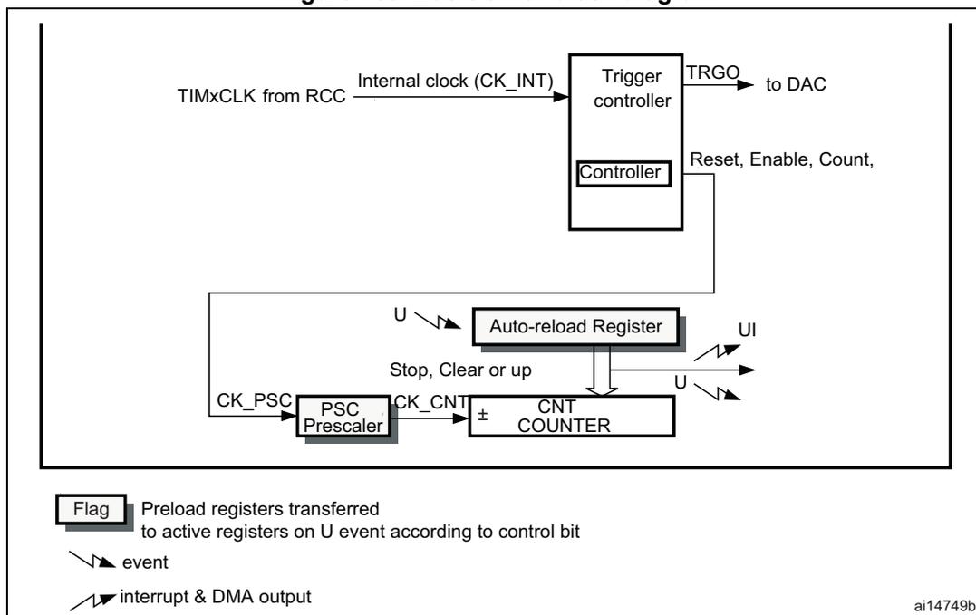
The basic timers TIM6 and TIM7 consist of a 16-bit auto-reload counter driven by a programmable prescaler.
They may be used as generic timers for time-base generation but they are also specifically used to drive the digital-to-analog converter (DAC). In fact, the timers are internally connected to the DAC and are able to drive it through their trigger outputs.
The timers are completely independent, and do not share any resources.
17.2 TIM6 and TIM7 main features
Basic timer (TIM6 and TIM7) features include:
- • 16-bit auto-reload upcounter
- • 16-bit programmable prescaler used to divide (also “on the fly”) the counter clock frequency by any factor between 1 and 65536
- • Synchronization circuit to trigger the DAC
- • Interrupt/DMA generation on the update event: counter overflow
Figure 169. Basic timer block diagram
17.3 TIM6 and TIM7 functional description
17.3.1 Time-base unit
The main block of the programmable timer is a 16-bit upcounter with its related auto-reload register. The counter clock can be divided by a prescaler.
The counter, the auto-reload register and the prescaler register can be written or read by software. This is true even when the counter is running.
The time-base unit includes:
- • Counter register (TIMx_CNT)
- • Prescaler register (TIMx_PSC)
- • Auto-Reload register (TIMx_ARR)
The auto-reload register is preloaded. The preload register is accessed each time an attempt is made to write or read the auto-reload register. The contents of the preload register are transferred into the shadow register permanently or at each update event UEV, depending on the auto-reload preload enable bit (ARPE) in the TIMx_CR1 register. The update event is sent when the counter reaches the overflow value and if the UDIS bit equals 0 in the TIMx_CR1 register. It can also be generated by software. The generation of the update event is described in detail for each configuration.
The counter is clocked by the prescaler output CK_CNT, which is enabled only when the counter enable bit (CEN) in the TIMx_CR1 register is set.
Note that the actual counter enable signal CNT_EN is set 1 clock cycle after CEN.
Prescaler description
The prescaler can divide the counter clock frequency by any factor between 1 and 65536. It is based on a 16-bit counter controlled through a 16-bit register (in the TIMx_PSC register). It can be changed on the fly as the TIMx_PSC control register is buffered. The new prescaler ratio is taken into account at the next update event.
Figure 170 and Figure 171 give some examples of the counter behavior when the prescaler ratio is changed on the fly.
Figure 170. Counter timing diagram with prescaler division change from 1 to 2
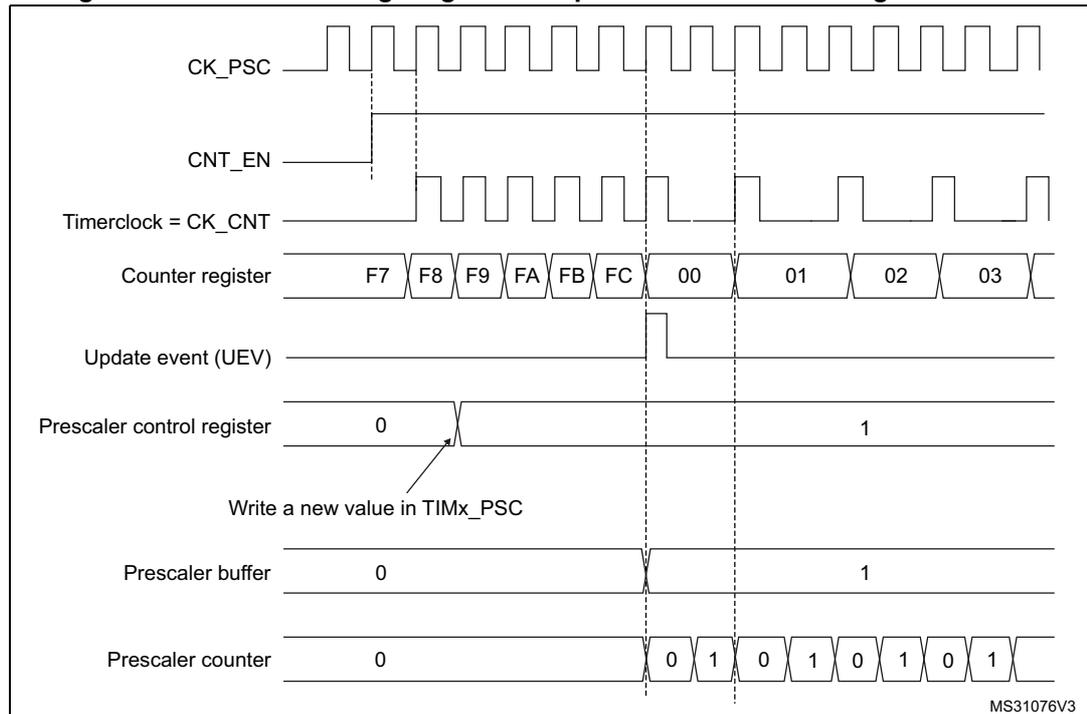
The timing diagram illustrates the behavior of a timer when the prescaler division is changed from 1 to 2. The diagram includes the following signals and registers over time:
- CK_PSC : A high-frequency square wave clock signal.
- CNT_EN : Counter Enable signal, which goes high to start the counter.
- Timerclock = CK_CNT : The clock signal for the counter, which is derived from CK_PSC. Its frequency changes when the prescaler division changes.
- Counter register : Shows the counter values. It counts from F7 to FC, then rolls over to 00, 01, 02, and 03. The rollover occurs at the Update Event (UEV).
- Update event (UEV) : A pulse that occurs when the counter rolls over, signaling the start of a new prescaler cycle.
- Prescaler control register : Initially set to 0 (division of 1). A write operation is performed to change it to 1 (division of 2). This change is not immediately effective.
- Write a new value in TIMx_PSC : An arrow indicates the point in time when the new prescaler value (1) is written to the control register.
- Prescaler buffer : A buffer that latches the new prescaler value from the control register. It updates its value to 1 at the next Update Event (UEV).
- Prescaler counter : A counter that divides the CK_PSC frequency. It counts from 0 to 0, 1, 0, 1, 0, 1, 0, 1. The change in the prescaler buffer value takes effect at the next UEV, causing the Timerclock (CK_CNT) frequency to halve.
MS31076V3
Figure 171. Counter timing diagram with prescaler division change from 1 to 4
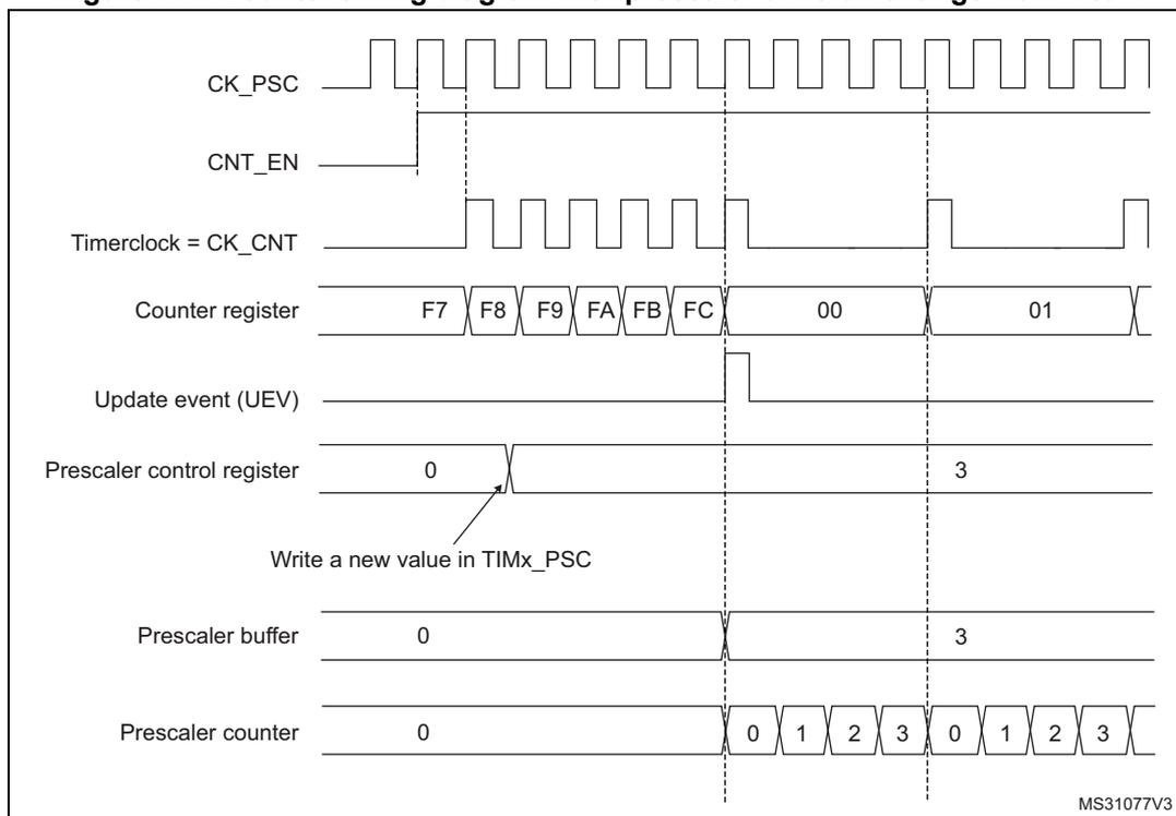
The diagram illustrates the timing of a basic timer (TIM6 or TIM7) when the prescaler division is changed from 1 to 4. The signals shown are:
- CK_PSC : System clock signal.
- CNT_EN : Counter enable signal, which is high to enable counting.
- Timerclock = CK_CNT : The clock signal for the counter, derived from CK_PSC divided by the prescaler value.
- Counter register : Shows the counter values. It counts from F7 to FC, then overflows to 00. After the prescaler change, it counts from 00 to 01.
- Update event (UEV) : A pulse generated when the counter overflows or when the UG bit is set in the TIMx_EGR register.
- Prescaler control register : Shows the value written to the TIMx_PSC register. It is initially 0, then changed to 3 (which corresponds to a division of 4).
- Prescaler buffer : A shadow register that holds the new prescaler value (3) until the next update event.
- Prescaler counter : A counter that divides the CK_PSC frequency by the value in the prescaler buffer. It counts from 0 to 3, then overflows to 0.
The diagram shows that when the prescaler control register is changed from 0 to 3, the prescaler buffer is updated to 3. The prescaler counter then counts from 0 to 3, generating an update event (UEV) when it overflows. This update event causes the counter register to be reloaded with the value 00. The timer clock (CK_CNT) frequency decreases after the prescaler change.
MS31077V3
17.3.2 Counting mode
The counter counts from 0 to the auto-reload value (contents of the TIMx_ARR register), then restarts from 0 and generates a counter overflow event.
An update event can be generated at each counter overflow or by setting the UG bit in the TIMx_EGR register (by software or by using the slave mode controller).
The UEV event can be disabled by software by setting the UDIS bit in the TIMx_CR1 register. This avoids updating the shadow registers while writing new values into the preload registers. In this way, no update event occurs until the UDIS bit has been written to 0, however, the counter and the prescaler counter both restart from 0 (but the prescale rate does not change). In addition, if the URS (update request selection) bit in the TIMx_CR1 register is set, setting the UG bit generates an update event UEV, but the UIF flag is not set (so no interrupt or DMA request is sent).
When an update event occurs, all the registers are updated and the update flag (UIF bit in the TIMx_SR register) is set (depending on the URS bit):
- • The buffer of the prescaler is reloaded with the preload value (contents of the TIMx_PSC register)
- • The auto-reload shadow register is updated with the preload value (TIMx_ARR)
The following figures show some examples of the counter behavior for different clock frequencies when TIMx_ARR = 0x36.
Figure 172. Counter timing diagram, internal clock divided by 1
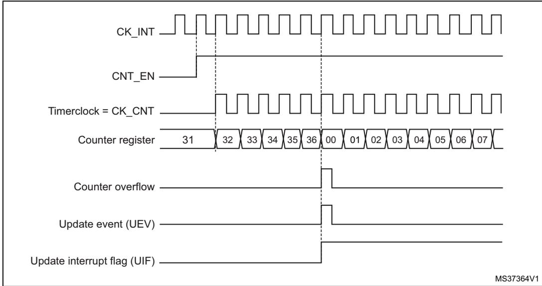
This timing diagram illustrates the operation of a timer with the internal clock divided by 1. The top signal, CK_INT, is a continuous square wave. Below it, CNT_EN is shown as a high-level signal. The Timerclock = CK_CNT signal is a square wave that follows the frequency of CK_INT. The Counter register is shown as a sequence of values: 31, 32, 33, 34, 35, 36, 00, 01, 02, 03, 04, 05, 06, 07. A Counter overflow pulse occurs when the counter transitions from 36 to 00. The Update event (UEV) and Update interrupt flag (UIF) are shown as pulses that coincide with the counter overflow. The diagram is labeled MS37364V1 in the bottom right corner.
Figure 173. Counter timing diagram, internal clock divided by 2
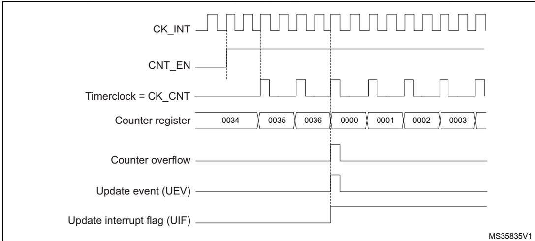
This timing diagram illustrates the operation of a timer with the internal clock divided by 2. The top signal, CK_INT, is a continuous square wave. Below it, CNT_EN is shown as a high-level signal. The Timerclock = CK_CNT signal is a square wave with half the frequency of CK_INT. The Counter register is shown as a sequence of values: 0034, 0035, 0036, 0000, 0001, 0002, 0003. A Counter overflow pulse occurs when the counter transitions from 0036 to 0000. The Update event (UEV) and Update interrupt flag (UIF) are shown as pulses that coincide with the counter overflow. The diagram is labeled MS35835V1 in the bottom right corner.
Figure 174. Counter timing diagram, internal clock divided by 4
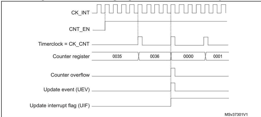
This timing diagram illustrates the operation of a timer when the internal clock is divided by 4. The top signal, CK_INT, is a high-frequency square wave. Below it, CNT_EN is a horizontal line indicating the counter is enabled. The Timerclock = CK_CNT signal is a square wave with a period four times that of CK_INT. The Counter register shows values 0035, 0036, 0000, and 0001. The Counter overflow signal goes high when the counter reaches 0000. The Update event (UEV) and Update interrupt flag (UIF) signals also go high at the overflow point. The diagram is labeled MSv37301V1 in the bottom right corner.
Figure 175. Counter timing diagram, internal clock divided by N
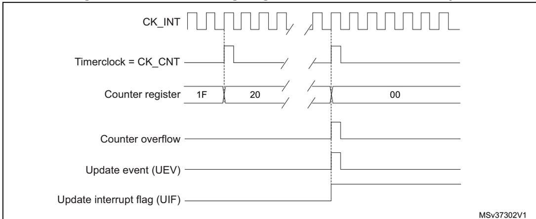
This timing diagram shows the timer operation with the internal clock divided by an arbitrary factor N. CK_INT is the internal clock, and Timerclock = CK_CNT is the divided clock. The Counter register shows values 1F, 20, and 00. The Counter overflow, Update event (UEV), and Update interrupt flag (UIF) signals all go high when the counter reaches 00. The diagram is labeled MSv37302V1 in the bottom right corner.
Figure 176. Counter timing diagram, update event when ARPE=0 (TIMx_ARR not preloaded)
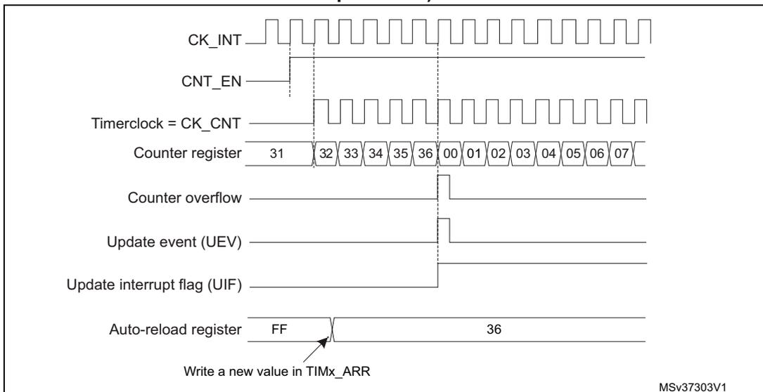
This timing diagram depicts the timer behavior when ARPE=0 and the TIMx_ARR register is not preloaded. CK_INT is the internal clock, and CNT_EN enables the counter. The Timerclock = CK_CNT is derived from CK_INT. The Counter register counts from 31 to 00, then overflows to 01, 02, 03, 04, 05, 06, and 07. The Counter overflow, Update event (UEV), and Update interrupt flag (UIF) signals go high at the 00 value. The Auto-reload register is shown with values FF and 36. An arrow points to the transition from FF to 36 with the text 'Write a new value in TIMx_ARR'. The diagram is labeled MSv37303V1 in the bottom right corner.
Figure 177. Counter timing diagram, update event when ARPE=1 (TIMx_ARR preloaded)
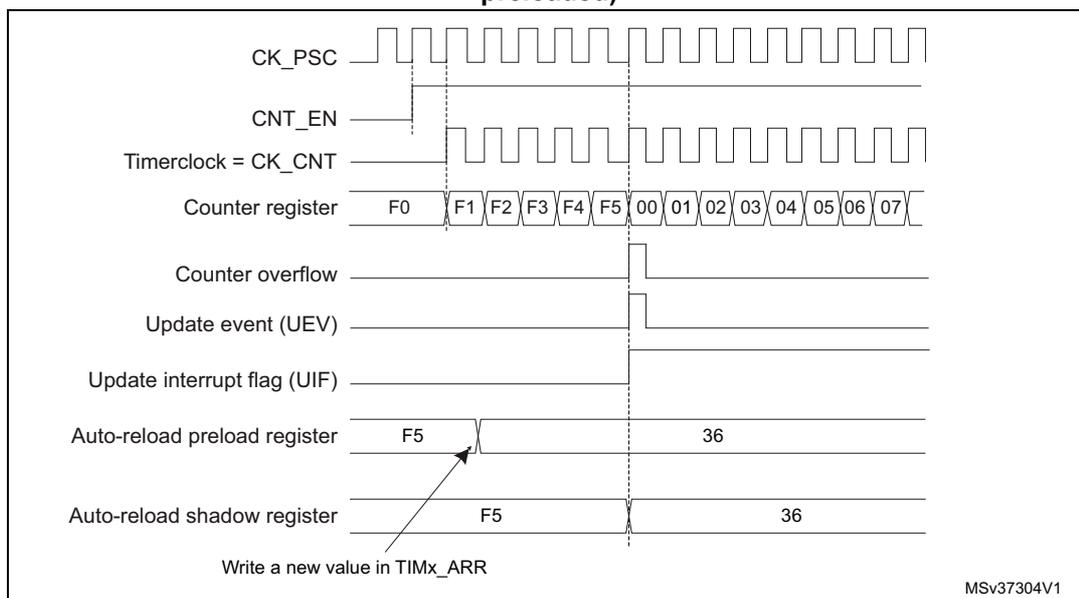
This timing diagram illustrates the operation of a timer counter when the ARPE (Auto-Reload Preload Enable) bit is set. The signals shown are:
- CK_PSC : Prescaler clock signal, a continuous square wave.
- CNT_EN : Counter enable signal, which goes high to start the counter.
- Timerclock = CK_CNT : The clock signal for the counter, derived from CK_PSC.
- Counter register : Shows the counter values incrementing: F0, F1, F2, F3, F4, F5. Upon the update event, it resets to 00 and continues 01, 02, 03, 04, 05, 06, 07.
- Counter overflow : A pulse generated when the counter reaches its maximum value (F5) before reloading.
- Update event (UEV) : A pulse generated at the overflow point that triggers the update of shadow registers.
- Update interrupt flag (UIF) : A flag that is set high by the update event.
- Auto-reload preload register : Initially contains F5. A write operation changes it to 36 mid-cycle.
- Auto-reload shadow register : Holds the value F5 until the update event (UEV), at which point it is updated to 36 from the preload register.
Text annotation: "Write a new value in TIMx_ARR" pointing to the change in the preload register.
Reference: MSv37304V1
17.3.3 Clock source
The counter clock is provided by the Internal clock (CK_INT) source.
The CEN (in the TIMx_CR1 register) and UG bits (in the TIMx_EGR register) are actual control bits and can be changed only by software (except for UG that remains cleared automatically). As soon as the CEN bit is written to 1, the prescaler is clocked by the internal clock CK_INT.
Figure 178 shows the behavior of the control circuit and the upcounter in normal mode, without prescaler.
Figure 178. Control circuit in normal mode, internal clock divided by 1
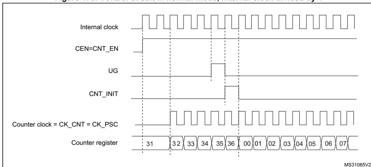
This timing diagram shows the control circuit and counter behavior in normal mode where the clock is not divided. The signals shown are:
- Internal clock : The source clock for the timer, a continuous square wave.
- CEN=CNT_EN : Counter enable signal, which goes high to enable counting.
- UG : Update generation bit, which is pulsed high by software to force an update.
- CNT_INIT : Counter initialization signal, which pulses high in response to the UG bit.
- Counter clock = CK_CNT = CK_PSC : The clock signal for the counter, which matches the internal clock.
- Counter register : Shows the counter values incrementing: 31, 32, 33, 34, 35, 36. When the UG bit is set, the counter is initialized to 00 on the next clock edge and continues 01, 02, 03, 04, 05, 06, 07.
Reference: MS31085V2
17.3.4 Debug mode
When the microcontroller enters the debug mode (Cortex®-M3 core - halted), the TIMx counter either continues to work normally or stops, depending on the DBG_TIMx_STOP configuration bit in the DBG module. For more details, refer to Section 31.16.2: Debug support for timers, watchdog, bxCAN and I 2 C .
17.4 TIM6 and TIM7 registers
Refer to Section 2.2 for a list of abbreviations used in register descriptions.
The peripheral registers have to be written by half-words (16 bits) or words (32 bits). Read accesses can be done by bytes (8 bits), half-words (16 bits) or words (32 bits).
17.4.1 TIM6 and TIM7 control register 1 (TIMx_CR1)
Address offset: 0x00
Reset value: 0x0000
| 15 | 14 | 13 | 12 | 11 | 10 | 9 | 8 | 7 | 6 | 5 | 4 | 3 | 2 | 1 | 0 |
|---|---|---|---|---|---|---|---|---|---|---|---|---|---|---|---|
| Reserved | ARPE | Reserved | OPM | URS | UDIS | CEN | |||||||||
| rw | rw | rw | rw | rw | |||||||||||
Bits 15:8 Reserved, must be kept at reset value.
Bit 7 ARPE : Auto-reload preload enable
0: TIMx_ARR register is not buffered.
1: TIMx_ARR register is buffered.
Bits 6:4 Reserved, must be kept at reset value.
Bit 3 OPM : One-pulse mode
0: Counter is not stopped at update event
1: Counter stops counting at the next update event (clearing the CEN bit).
Bit 2 URS: Update request sourceThis bit is set and cleared by software to select the UEV event sources.
0: Any of the following events generates an update interrupt or DMA request if enabled.
These events can be:
- – Counter overflow/underflow
- – Setting the UG bit
- – Update generation through the slave mode controller
1: Only counter overflow/underflow generates an update interrupt or DMA request if enabled.
Bit 1 UDIS: Update disableThis bit is set and cleared by software to enable/disable UEV event generation.
0: UEV enabled. The Update (UEV) event is generated by one of the following events:
- – Counter overflow/underflow
- – Setting the UG bit
- – Update generation through the slave mode controller
Buffered registers are then loaded with their preload values.
1: UEV disabled. The Update event is not generated, shadow registers keep their value (ARR, PSC). However the counter and the prescaler are reinitialized if the UG bit is set or if a hardware reset is received from the slave mode controller.
Bit 0 CEN: Counter enable0: Counter disabled
1: Counter enabled
Note: Gated mode can work only if the CEN bit has been previously set by software. However trigger mode can set the CEN bit automatically by hardware.
CEN is cleared automatically in one-pulse mode, when an update event occurs.
17.4.2 TIM6 and TIM7 control register 2 (TIMx_CR2)
Address offset: 0x04
Reset value: 0x0000

| 15 | 14 | 13 | 12 | 11 | 10 | 9 | 8 | 7 | 6 | 5 | 4 | 3 | 2 | 1 | 0 |
| Reserved | MMS[2:0] | Reserved | |||||||||||||
| rw | rw | rw | |||||||||||||
Bits 15:7 Reserved, must be kept at reset value.
Bits 6:4 MMS[2:0] : Master mode selectionThese bits are used to select the information to be sent in master mode to slave timers for synchronization (TRGO). The combination is as follows:
000: Reset - the UG bit from the TIMx_EGR register is used as a trigger output (TRGO). If reset is generated by the trigger input (slave mode controller configured in reset mode) then the signal on TRGO is delayed compared to the actual reset.
001: Enable - the Counter enable signal, CNT_EN, is used as a trigger output (TRGO). It is useful to start several timers at the same time or to control a window in which a slave timer is enabled. The Counter Enable signal is generated by a logic OR between CEN control bit and the trigger input when configured in gated mode.
When the Counter Enable signal is controlled by the trigger input, there is a delay on TRGO, except if the master/slave mode is selected (see the MSM bit description in the TIMx_SMCR register).
010: Update - The update event is selected as a trigger output (TRGO). For instance a master timer can then be used as a prescaler for a slave timer.
Note: The clock of the slave timer and ADC must be enabled prior to receiving events from the master timer, and must not be changed on-the-fly while triggers are received from the master timer.
Bits 3:0 Reserved, must be kept at reset value.
17.4.3 TIM6 and TIM7 DMA/Interrupt enable register (TIMx_DIER)
Address offset: 0x0C
Reset value: 0x0000

| 15 | 14 | 13 | 12 | 11 | 10 | 9 | 8 | 7 | 6 | 5 | 4 | 3 | 2 | 1 | 0 |
| Reserved | UDE | Reserved | UIE | ||||||||||||
| rw | rw | ||||||||||||||
Bits 15:9 Reserved, must be kept at reset value.
Bit 8 UDE : Update DMA request enable0: Update DMA request disabled.
1: Update DMA request enabled.
Bits 7:1 Reserved, must be kept at reset value.
Bit 0 UIE : Update interrupt enable0: Update interrupt disabled.
1: Update interrupt enabled.
17.4.4 TIM6 and TIM7 status register (TIMx_SR)
Address offset: 0x10
Reset value: 0x0000

| 15 | 14 | 13 | 12 | 11 | 10 | 9 | 8 | 7 | 6 | 5 | 4 | 3 | 2 | 1 | 0 |
| Reserved | UIF | ||||||||||||||
| rc_w0 | |||||||||||||||
Bits 15:1 Reserved, must be kept at reset value.
Bit 0 UIF : Update interrupt flag
This bit is set by hardware on an update event. It is cleared by software.
0: No update occurred.
1: Update interrupt pending. This bit is set by hardware when the registers are updated:
- – At overflow or underflow and if UDIS = 0 in the TIMx_CR1 register.
- – When CNT is reinitialized by software using the UG bit in the TIMx_EGR register, if URS = 0 and UDIS = 0 in the TIMx_CR1 register.
17.4.5 TIM6 and TIM7 event generation register (TIMx_EGR)
Address offset: 0x14
Reset value: 0x0000

| 15 | 14 | 13 | 12 | 11 | 10 | 9 | 8 | 7 | 6 | 5 | 4 | 3 | 2 | 1 | 0 |
| Reserved | UG | ||||||||||||||
| w | |||||||||||||||
Bits 15:1 Reserved, must be kept at reset value.
Bit 0 UG : Update generation
This bit can be set by software, it is automatically cleared by hardware.
0: No action.
1: Re-initializes the timer counter and generates an update of the registers. Note that the prescaler counter is cleared too (but the prescaler ratio is not affected).
17.4.6 TIM6 and TIM7 counter (TIMx_CNT)
Address offset: 0x24
Reset value: 0x0000

| 15 | 14 | 13 | 12 | 11 | 10 | 9 | 8 | 7 | 6 | 5 | 4 | 3 | 2 | 1 | 0 |
| CNT[15:0] | |||||||||||||||
| rw | rw | rw | rw | rw | rw | rw | rw | rw | rw | rw | rw | rw | rw | rw | rw |
Bits 15:0 CNT[15:0] : Counter value
17.4.7 TIM6 and TIM7 prescaler (TIMx_PSC)
Address offset: 0x28
Reset value: 0x0000

| 15 | 14 | 13 | 12 | 11 | 10 | 9 | 8 | 7 | 6 | 5 | 4 | 3 | 2 | 1 | 0 |
| PSC[15:0] | |||||||||||||||
| rw | rw | rw | rw | rw | rw | rw | rw | rw | rw | rw | rw | rw | rw | rw | rw |
Bits 15:0 PSC[15:0] : Prescaler value
The counter clock frequency \( f_{CK\_CNT} \) is equal to \( f_{CK\_PSC} / (PSC[15:0] + 1) \) .
PSC contains the value to be loaded in the active prescaler register at each update event (including when the counter is cleared through UG bit of TIMx_EGR register or through trigger controller when configured in “reset mode”).
17.4.8 TIM6 and TIM7 auto-reload register (TIMx_ARR)
Address offset: 0x2C
Reset value: 0xFFFF

| 15 | 14 | 13 | 12 | 11 | 10 | 9 | 8 | 7 | 6 | 5 | 4 | 3 | 2 | 1 | 0 |
| ARR[15:0] | |||||||||||||||
| rw | rw | rw | rw | rw | rw | rw | rw | rw | rw | rw | rw | rw | rw | rw | rw |
Bits 15:0 ARR[15:0] : Auto-reload value
ARR is the value to be loaded into the actual auto-reload register.
Refer to Section 17.3.1: Time-base unit for more details about ARR update and behavior.
The counter is blocked while the auto-reload value is null.
17.4.9 TIM6 and TIM7 register map
TIMx registers are mapped as 16-bit addressable registers as described in the table below.
Table 94. TIM6 and TIM7 register map and reset values
| Offset | Register | 31 | 30 | 29 | 28 | 27 | 26 | 25 | 24 | 23 | 22 | 21 | 20 | 19 | 18 | 17 | 16 | 15 | 14 | 13 | 12 | 11 | 10 | 9 | 8 | 7 | 6 | 5 | 4 | 3 | 2 | 1 | 0 |
|---|---|---|---|---|---|---|---|---|---|---|---|---|---|---|---|---|---|---|---|---|---|---|---|---|---|---|---|---|---|---|---|---|---|
| 0x00 | TIMx_CR1 | Reserved | ARPE | Reserved | OPM | URS | UDIS | CEN | |||||||||||||||||||||||||
| Reset value | 0 | 0 | 0 | 0 | 0 | ||||||||||||||||||||||||||||
| 0x04 | TIMx_CR2 | Reserved | |||||||||||||||||||||||||||||||
| Reset value | |||||||||||||||||||||||||||||||||
| 0x08 | Reserved | ||||||||||||||||||||||||||||||||
| 0x0C | TIMx_DIER | Reserved | UDE | Reserved | UIE | ||||||||||||||||||||||||||||
| Reset value | 0 | 0 | |||||||||||||||||||||||||||||||
| 0x10 | TIMx_SR | Reserved | UIF | ||||||||||||||||||||||||||||||
| Reset value | 0 | ||||||||||||||||||||||||||||||||
| 0x14 | TIMx_EGR | Reserved | UG | ||||||||||||||||||||||||||||||
| Reset value | 0 | ||||||||||||||||||||||||||||||||
| 0x18 | Reserved | ||||||||||||||||||||||||||||||||
| 0x1C | Reserved | ||||||||||||||||||||||||||||||||
| 0x20 | Reserved | ||||||||||||||||||||||||||||||||
| 0x24 | TIMx_CNT | Reserved | CNT[15:0] | ||||||||||||||||||||||||||||||
| Reset value | 0 0 0 0 0 0 0 0 0 0 0 0 0 0 0 0 | ||||||||||||||||||||||||||||||||
| 0x28 | TIMx_PSC | Reserved | PSC[15:0] | ||||||||||||||||||||||||||||||
| Reset value | 0 0 0 0 0 0 0 0 0 0 0 0 0 0 0 0 | ||||||||||||||||||||||||||||||||
| 0x2C | TIMx_ARR | Reserved | ARR[15:0] | ||||||||||||||||||||||||||||||
| Reset value | 1 1 1 1 1 1 1 1 1 1 1 1 1 1 1 1 | ||||||||||||||||||||||||||||||||
Refer to Section 3.3: Memory map for the register boundary addresses.