11. Analog-to-digital converter (ADC)
Low-density devices are STM32F101xx, STM32F102xx and STM32F103xx microcontrollers where the Flash memory density ranges between 16 and 32 Kbytes.
Medium-density devices are STM32F101xx, STM32F102xx and STM32F103xx microcontrollers where the Flash memory density ranges between 64 and 128 Kbytes.
High-density devices are STM32F101xx and STM32F103xx microcontrollers where the Flash memory density ranges between 256 and 512 Kbytes.
XL-density devices are STM32F101xx and STM32F103xx microcontrollers where the Flash memory density ranges between 768 Kbytes and 1 Mbyte.
Connectivity line devices are STM32F105xx and STM32F107xx microcontrollers.
This section applies to the whole STM32F10xxx family, unless otherwise specified.
11.1 ADC introduction
The 12-bit ADC is a successive approximation analog-to-digital converter. It has up to 18 multiplexed channels allowing it measure signals from sixteen external and two internal sources. A/D conversion of the various channels can be performed in single, continuous, scan or discontinuous mode. The result of the ADC is stored in a left-aligned or right-aligned 16-bit data register.
The analog watchdog feature allows the application to detect if the input voltage goes outside the user-defined high or low thresholds.
The ADC input clock is generated from the PCLK2 clock divided by a prescaler and it must not exceed 14 MHz, refer to Figure 8 for low-, medium-, high- and XL-density devices, and to Figure 11 for connectivity line devices.
11.2 ADC main features
- • 12-bit resolution
- • Interrupt generation at End of Conversion, End of Injected conversion and Analog watchdog event
- • Single and continuous conversion modes
- • Scan mode for automatic conversion of channel 0 to channel 'n'
- • Self-calibration
- • Data alignment with in-built data coherency
- • Channel by channel programmable sampling time
- • External trigger option for both regular and injected conversion
- • Discontinuous mode
- • Dual mode (on devices with 2 ADCs or more)
- • ADC conversion time:
- – STM32F103xx performance line devices: 1 µs at 56 MHz (1.17 µs at 72 MHz)
- – STM32F101xx access line devices: 1 µs at 28 MHz (1.55 µs at 36 MHz)
- – STM32F102xx USB access line devices: 1.2 µs at 48 MHz
- – STM32F105xx and STM32F107xx devices: 1 µs at 56 MHz (1.17 µs at 72 MHz)
- • ADC supply requirement: 2.4 V to 3.6 V
- • ADC input range: \( V_{REF-} \leq V_{IN} \leq V_{REF+} \)
- • DMA request generation during regular channel conversion
The block diagram of the ADC is shown in Figure 22 .
Note: \( V_{REF-} \) , if available (depending on package), must be tied to \( V_{SSA} \) .
11.3 ADC functional description
Figure 22 shows a single ADC block diagram and Table 65 gives the ADC pin description.
Figure 22. Single ADC block diagram
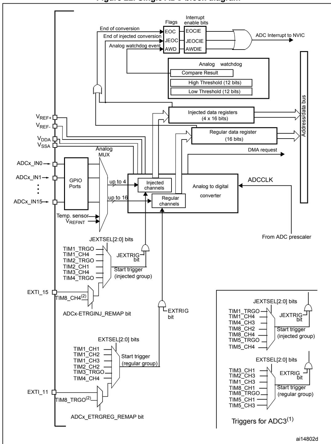
The diagram illustrates the internal architecture of an ADC. On the left, input sources include \( V_{REF+} \) , \( V_{REF-} \) , \( V_{DDA} \) , and \( V_{SSA} \) . External pins \( ADCx\_IN0 \) through \( ADCx\_IN15 \) connect to GPIO Ports, which are then routed through an Analog MUX. A temperature sensor ( \( V_{REFINT} \) ) is also connected to this MUX. The MUX outputs are split into 'Injected channels' (up to 4) and 'Regular channels' (up to 16), which then feed into the 'Analog to digital converter' block. This block is clocked by \( ADCCLK \) (from an ADC prescaler) and receives data via an 'Address/data bus'. The converter generates 'End of conversion' (EOC), 'End of injected conversion' (JEOC), and 'Analog watchdog event' (AWD) signals. These are processed through 'Flags' and 'Interrupt enable bits' (EOCIE, JEOCIE, AWDIE) to generate an 'ADC Interrupt to NVIC'. The 'Analog watchdog' block contains 'Compare Result', 'High Threshold (12 bits)', and 'Low Threshold (12 bits)'. Conversion results are stored in 'Injected data registers (4 x 16 bits)' and a 'Regular data register (16 bits)', which are also connected to the 'Address/data bus' and can generate a 'DMA request'. External triggers are provided by TIM1, TIM2, TIM3, TIM4, TIM5, and TIM8. For the injected group, triggers include TIM1_TRGO, TIM1_CH4, TIM2_TRGO, TIM2_CH1, TIM3_CH4, TIM4_TRGO, and TIM8_CH4 (2) , controlled by JEXTSEL[2:0] bits and JEXTRIG bit. For the regular group, triggers include TIM1_CH1, TIM1_CH2, TIM1_CH3, TIM2_CH2, TIM3_TRGO, TIM4_CH4, and TIM8_TRGO (2) , controlled by EXTSEL[2:0] bits and EXTRIG bit. Remap bits \( ADCx\_ETRGINJ\_REMAP \) and \( ADCx\_ETRGREG\_REMAP \) are also shown. A detailed view of the triggers for ADC3 (1) is provided in a separate box on the right.
- 1. ADC3 has regular and injected conversion triggers different from those of ADC1 and ADC2.
- 2. TIM8_CH4 and TIM8_TRGO with their corresponding remap bits exist only in High-density and XL-density products.
Table 65. ADC pins
| Name | Signal type | Remarks |
|---|---|---|
| V REF+ | Input, analog reference positive | The higher/positive reference voltage for the ADC, \( 2.4 \text{ V} \leq V_{\text{REF+}} \leq V_{\text{DDA}} \) |
| V DDA (1) | Input, analog supply | Analog power supply equal to V DD and \( 2.4 \text{ V} \leq V_{\text{DDA}} \leq 3.6 \text{ V} \) |
| V REF- | Input, analog reference negative | The lower/negative reference voltage for the ADC, \( V_{\text{REF-}} = V_{\text{SSA}} \) |
| V SSA (1) | Input, analog supply ground | Ground for analog power supply equal to V SS |
| ADCx_IN[15:0] | Analog signals | Up to 21 analog channels (2) |
1. V DDA and V SSA have to be connected to V DD and V SS , respectively.
2. For full details about the ADC I/O pins, refer to the “Pinouts and pin descriptions” section of the corresponding device datasheet.
11.3.1 ADC on-off control
The ADC can be powered-on by setting the ADON bit in the ADC_CR2 register. When the ADON bit is set for the first time, it wakes up the ADC from Power Down mode.
Conversion starts when ADON bit is set for a second time by software after ADC power-up time ( \( t_{\text{STAB}} \) ).
The conversion can be stopped, and the ADC put in power down mode by resetting the ADON bit. In this mode the ADC consumes almost no power (only a few \( \mu\text{A} \) ).
11.3.2 ADC clock
The ADCCLK clock provided by the Clock Controller is synchronous with the PCLK2 (APB2 clock). The RCC controller has a dedicated programmable prescaler for the ADC clock, refer to Low-, medium-, high- and XL-density reset and clock control (RCC) for more details.
11.3.3 Channel selection
There are 16 multiplexed channels. It is possible to organize the conversions in two groups: regular and injected. A group consists of a sequence of conversions which can be done on any channel and in any order. For instance, it is possible to do the conversion in the following order: Ch3, Ch8, Ch2, Ch2, Ch0, Ch2, Ch2, Ch15.
- • The regular group is composed of up to 16 conversions. The regular channels and their order in the conversion sequence must be selected in the ADC_SQRx registers. The total number of conversions in the regular group must be written in the L[3:0] bits in the ADC_SQR1 register.
- • The injected group is composed of up to 4 conversions. The injected channels and their order in the conversion sequence must be selected in the ADC_JSQR register. The total number of conversions in the injected group must be written in the L[1:0] bits in the ADC_JSQR register.
If the ADC_SQRx or ADC_JSQR registers are modified during a conversion, the current conversion is reset and a new start pulse is sent to the ADC to convert the new chosen group.
Temperature sensor/ \( V_{REFINT} \) internal channels
The temperature sensor is connected to channel ADCx_IN16 and the internal reference voltage \( V_{REFINT} \) is connected to ADCx_IN17. These two internal channels can be selected and converted as injected or regular channels.
Note: The sensor and \( V_{REFINT} \) are only available on the master ADC1 peripheral.
11.3.4 Single conversion mode
In Single conversion mode the ADC does one conversion. This mode is started either by setting the ADON bit in the ADC_CR2 register (for a regular channel only) or by external trigger (for a regular or injected channel), while the CONT bit is 0.
Once the conversion of the selected channel is complete:
- • If a regular channel was converted:
- – The converted data is stored in the 16-bit ADC_DR register
- – The EOC (End Of Conversion) flag is set
- – and an interrupt is generated if the EOCIE is set.
- • If an injected channel was converted:
- – The converted data is stored in the 16-bit ADC_DRJ1 register
- – The JEOC (End Of Conversion Injected) flag is set
- – and an interrupt is generated if the JEOCIE bit is set.
The ADC is then stopped.
11.3.5 Continuous conversion mode
In continuous conversion mode ADC starts another conversion as soon as it finishes one. This mode is started either by external trigger or by setting the ADON bit in the ADC_CR2 register, while the CONT bit is 1.
After each conversion:
- • If a regular channel was converted:
- – The converted data is stored in the 16-bit ADC_DR register
- – The EOC (End Of Conversion) flag is set
- – An interrupt is generated if the EOCIE is set.
- • If an injected channel was converted:
- – The converted data is stored in the 16-bit ADC_DRJ1 register
- – The JEOC (End Of Conversion Injected) flag is set
- – An interrupt is generated if the JEOCIE bit is set.
11.3.6 Timing diagram
As shown in Figure 23 , the ADC needs a stabilization time of \( t_{STAB} \) before it starts converting accurately. After the start of ADC conversion and after 14 clock cycles, the EOC flag is set and the 16-bit ADC Data register contains the result of the conversion.
Figure 23. Timing diagram
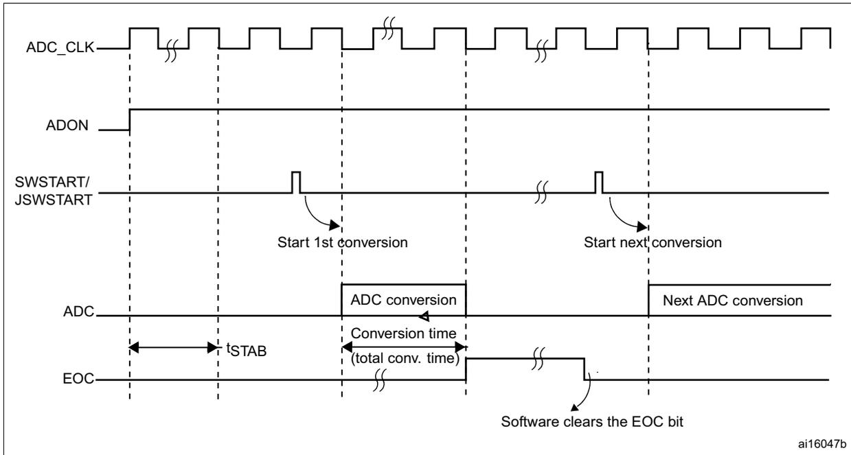
The timing diagram shows the relationship between several signals during an ADC conversion sequence.
1.
ADC_CLK
: A periodic clock signal.
2.
ADON
: A signal that goes high to enable the ADC.
3.
SWSTART/JSWSTART
: A signal that pulses high to start a conversion. The first pulse is labeled 'Start 1st conversion' and the second 'Start next conversion'.
4.
ADC
: The analog-to-digital converter output. It shows a period labeled 'ADC conversion' followed by 'Conversion time (total conv. time)'.
5.
EOC
: End of Conversion signal. It goes high when the conversion is complete and is later shown being cleared by software.
A time interval
t
STAB
is indicated between the rising edge of ADON and the start of the first conversion.
The diagram is labeled ai16047b.
11.3.7 Analog watchdog
The AWD analog watchdog status bit is set if the analog voltage converted by the ADC is below a low threshold or above a high threshold. These thresholds are programmed in the 12 least significant bits of the ADC_HTR and ADC_LTR 16-bit registers. An interrupt can be enabled by using the AWDIE bit in the ADC_CR1 register.
The threshold value is independent of the alignment selected by the ALIGN bit in the ADC_CR2 register. The comparison is done before the alignment (see Section 11.5 ).
The analog watchdog can be enabled on one or more channels by configuring the ADC_CR1 register as shown in Table 66 .
Figure 24. Analog watchdog guarded area

The graph shows 'Analog voltage' on the vertical axis. Two horizontal lines represent the 'Higher threshold' (HTR) and 'Lower threshold' (LTR). The region between these two thresholds is shaded and labeled 'Guarded area'. The diagram is labeled ai16048.
Table 66. Analog watchdog channel selection
| Channels to be guarded by analog watchdog | ADC_CR1 register control bits (x = don't care) | ||
|---|---|---|---|
| AWDSGL bit | AWDEN bit | JAWDEN bit | |
| None | x | 0 | 0 |
| All injected channels | 0 | 0 | 1 |
| All regular channels | 0 | 1 | 0 |
Table 66. Analog watchdog channel selection (continued)
| Channels to be guarded by analog watchdog | ADC_CR1 register control bits (x = don't care) | ||
|---|---|---|---|
| AWDSGL bit | AWDEN bit | JAWDEN bit | |
| All regular and injected channels | 0 | 1 | 1 |
| Single (1) injected channel | 1 | 0 | 1 |
| Single (1) regular channel | 1 | 1 | 0 |
| Single (1) regular or injected channel | 1 | 1 | 1 |
1. Selected by AWDCH[4:0] bits
11.3.8 Scan mode
This mode is used to scan a group of analog channels.
Scan mode can be selected by setting the SCAN bit in the ADC_CR1 register. Once this bit is set, ADC scans all the channels selected in the ADC_SQRx registers (for regular channels) or in the ADC_JSQR (for injected channels). A single conversion is performed for each channel of the group. After each end of conversion the next channel of the group is converted automatically. If the CONT bit is set, conversion does not stop at the last selected group channel but continues again from the first selected group channel.
When using scan mode, DMA bit must be set and the direct memory access controller is used to transfer the converted data of regular group channels to SRAM after each update of the ADC_DR register.
The injected channel converted data is always stored in the ADC_JDRx registers.
11.3.9 Injected channel management
Triggered injection
To use triggered injection, the JAUTO bit must be cleared and SCAN bit must be set in the ADC_CR1 register.
- 1. Start conversion of a group of regular channels either by external trigger or by setting the ADON bit in the ADC_CR2 register.
- 2. If an external injected trigger occurs during the regular group channel conversion, the current conversion is reset and the injected channel sequence is converted in Scan once mode.
- 3. Then, the regular group channel conversion is resumed from the last interrupted regular conversion. If a regular event occurs during an injected conversion, it doesn't interrupt it but the regular sequence is executed at the end of the injected sequence.
Figure 25 shows the timing diagram.
Note: When using triggered injection, the interval between trigger events must be longer than the injection sequence. For instance, if the sequence length is 28 ADC clock cycles (that is two conversions with a 1.5 clock-period sampling time), the minimum interval between triggers must be 29 ADC clock cycles.
Auto-injection
If the JAUTO bit is set, then the injected group channels are automatically converted after the regular group channels. This can be used to convert a sequence of up to 20 conversions programmed in the ADC_SQRx and ADC_JSQR registers.
In this mode, external trigger on injected channels must be disabled.
If the CONT bit is also set in addition to the JAUTO bit, regular channels followed by injected channels are continuously converted.
For ADC clock prescalers ranging from 4 to 8, a delay of 1 ADC clock period is automatically inserted when switching from regular to injected sequence (respectively injected to regular). When the ADC clock prescaler is set to 2, the delay is 2 ADC clock periods.
Note: It is not possible to use both auto-injected and discontinuous modes simultaneously.
Figure 25. Injected conversion latency
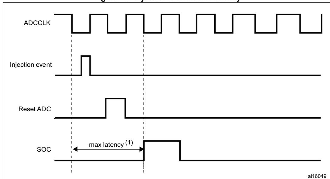
The figure is a timing diagram with four horizontal signal lines. From top to bottom, they are:
- ADCCLK : A periodic square wave clock signal.
- Injection event : A signal that goes high for a short duration, then returns to low. A vertical dashed line marks its rising edge.
- Reset ADC : A signal that goes high for a short duration, then returns to low. A vertical dashed line marks its rising edge.
- SOC : A signal that goes high when a conversion starts and returns to low when it ends. A vertical dashed line marks its rising edge.
- 1. The maximum latency value can be found in the electrical characteristics of the STM32F101xx and STM32F103xx datasheets.
11.3.10 Discontinuous mode
Regular group
This mode is enabled by setting the DISCEN bit in the ADC_CR1 register. It can be used to convert a short sequence of n conversions ( \( n \leq 8 \) ) which is a part of the sequence of conversions selected in the ADC_SQRx registers. The value of n is specified by writing to the DISCNUM[2:0] bits in the ADC_CR1 register.
When an external trigger occurs, it starts the next n conversions selected in the ADC_SQRx registers until all the conversions in the sequence are done. The total sequence length is defined by the L[3:0] bits in the ADC_SQR1 register.
Example:
n = 3, channels to be converted = 0, 1, 2, 3, 6, 7, 9, 10
first trigger: sequence converted 0, 1, 2. An EOC event is generated at each
conversion
second trigger: sequence converted 3, 6, 7. An EOC event is generated at each conversion
third trigger: sequence converted 9, 10. An EOC event is generated at each conversion
fourth trigger: sequence converted 0, 1, 2. An EOC event is generated at each conversion
Note:
When a regular group is converted in discontinuous mode, no rollover will occur. When all sub groups are converted, the next trigger starts conversion of the first sub-group.
In the example above, the fourth trigger reconverts the first sub-group channels 0, 1 and 2.
Injected group
This mode is enabled by setting the JDISCEN bit in the ADC_CR1 register. It can be used to convert the sequence selected in the ADC_JSQR register, channel by channel, after an external trigger event.
When an external trigger occurs, it starts the next channel conversions selected in the ADC_JSQR registers until all the conversions in the sequence are done. The total sequence length is defined by the JL[1:0] bits in the ADC_JSQR register.
Example:
n = 1, channels to be converted = 1, 2, 3
first trigger: channel 1 converted
second trigger: channel 2 converted
third trigger: channel 3 converted and EOC and JEOC events generated
fourth trigger: channel 1
Note:
When all injected channels are converted, the next trigger starts the conversion of the first injected channel. In the example above, the fourth trigger reconverts the first injected channel 1.
It is not possible to use both auto-injected and discontinuous modes simultaneously.
The user must avoid setting discontinuous mode for both regular and injected groups together. Discontinuous mode must be enabled only for one group conversion.
11.4 Calibration
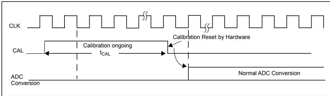
The ADC has an built-in self calibration mode. Calibration significantly reduces accuracy errors due to internal capacitor bank variations. During calibration, an error-correction code (digital word) is calculated for each capacitor, and during all subsequent conversions, the error contribution of each capacitor is removed using this code.
Calibration is started by setting the CAL bit in the ADC_CR2 register. Once calibration is over, the CAL bit is reset by hardware and normal conversion can be performed. It is recommended to calibrate the ADC once at power-on. The calibration codes are stored in the ADC_DR as soon as the calibration phase ends.
Note:
It is recommended to perform a calibration after each power-up.
Before starting a calibration, the ADC must have been in power-on state (ADON bit = '1') for at least two ADC clock cycles.
Figure 26. Calibration timing diagram
11.5 Data alignment
ALIGN bit in the ADC_CR2 register selects the alignment of data stored after conversion. Data can be left or right aligned as shown in Figure 27. and Figure 28.
The injected group channels converted data value is decreased by the user-defined offset written in the ADC_JOFRx registers so the result can be a negative value. The SEXT bit is the extended sign value.
For regular group channels no offset is subtracted so only twelve bits are significant.
Figure 27. Right alignment of data
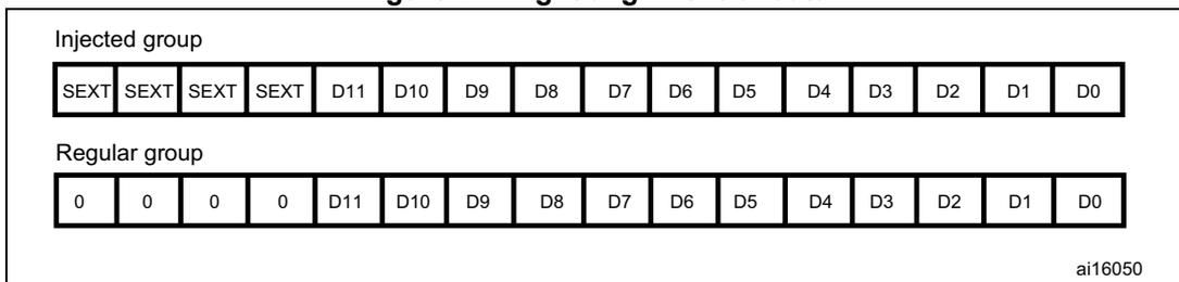
| Injected group | |||||||||||||||
| SEXT | SEXT | SEXT | SEXT | D11 | D10 | D9 | D8 | D7 | D6 | D5 | D4 | D3 | D2 | D1 | D0 |
| Regular group | |||||||||||||||
| 0 | 0 | 0 | 0 | D11 | D10 | D9 | D8 | D7 | D6 | D5 | D4 | D3 | D2 | D1 | D0 |
ai16050
Figure 28. Left alignment of data
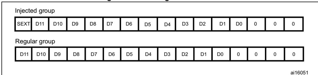
| Injected group | |||||||||||||||
| SEXT | D11 | D10 | D9 | D8 | D7 | D6 | D5 | D4 | D3 | D2 | D1 | D0 | 0 | 0 | 0 |
| Regular group | |||||||||||||||
| D11 | D10 | D9 | D8 | D7 | D6 | D5 | D4 | D3 | D2 | D1 | D0 | 0 | 0 | 0 | 0 |
ai16051
11.6 Channel-by-channel programmable sample time
ADC samples the input voltage for a number of ADC_CLK cycles which can be modified using the SMP[2:0] bits in the ADC_SMPR1 and ADC_SMPR2 registers. Each channel can be sampled with a different sample time.
The total conversion time is calculated as follows:
Example:
With an ADCCLK = 14 MHz and a sampling time of 1.5 cycles:
11.7 Conversion on external trigger
Conversion can be triggered by an external event (e.g. timer capture, EXTI line). If the EXT-TRIG control bit is set then external events are able to trigger a conversion. The EXTSEL[2:0] and JEXTSEL[2:0] control bits allow the application to select decide which out of 8 possible events can trigger conversion for the regular and injected groups.
Note: When an external trigger is selected for ADC regular or injected conversion, only the rising edge of the signal can start the conversion.
Table 67. External trigger for regular channels for ADC1 and ADC2
| Source | Type | EXTSEL[2:0] |
|---|---|---|
| TIM1_CC1 event | Internal signal from on-chip timers | 000 |
| TIM1_CC2 event | 001 | |
| TIM1_CC3 event | 010 | |
| TIM2_CC2 event | 011 | |
| TIM3_TRGO event | 100 | |
| TIM4_CC4 event | 101 | |
| EXTI line 11 / TIM8_TRGO event (1)(2) | External pin / Internal signal from on-chip timers | 110 |
| SWSTART | Software control bit | 111 |
1. The TIM8_TRGO event exists only in high-density and XL-density devices.
2. The selection of the external trigger EXTI line11 or TIM8_TRGO event for regular channels is done, respectively, through configuration bits ADC1_ETRGREG_REMAP and ADC2_ETRGREG_REMAP for ADC1 and ADC2.
Table 68. External trigger for injected channels for ADC1 and ADC2| Source | Connection type | JEXTSEL[2:0] |
|---|---|---|
| TIM1_TRGO event | Internal signal from on-chip timers | 000 |
| TIM1_CC4 event | 001 | |
| TIM2_TRGO event | 010 | |
| TIM2_CC1 event | 011 | |
| TIM3_CC4 event | 100 | |
| TIM4_TRGO event | 101 | |
| EXTI line 15/TIM8_CC4 event (1)(2) | External pin/Internal signal from on-chip timers | 110 |
| JSWSTART | Software control bit | 111 |
- 1. The TIM8_CC4 event exists only in high-density and XL-density devices.
- 2. The selection of the external trigger EXTI line15 or TIM8_CC4 event for injected channels is done through configuration bits ADC1_ETRGINJ_REMAP and ADC2_ETRGINJ_REMAP for ADC1 and ADC2, respectively.
| Source | Connection type | EXTSEL[2:0] |
|---|---|---|
| TIM3_CC1 event | Internal signal from on-chip timers | 000 |
| TIM2_CC3 event | 001 | |
| TIM1_CC3 event | 010 | |
| TIM8_CC1 event | 011 | |
| TIM8_TRGO event | 100 | |
| TIM5_CC1 event | 101 | |
| TIM5_CC3 event | 110 | |
| SWSTART | Software control bit | 111 |
| Source | Connection type | JEXTSEL[2:0] |
|---|---|---|
| TIM1_TRGO event | Internal signal from on-chip timers | 000 |
| TIM1_CC4 event | 001 | |
| TIM4_CC3 event | 010 | |
| TIM8_CC2 event | 011 | |
| TIM8_CC4 event | 100 | |
| TIM5_TRGO event | 101 | |
| TIM5_CC4 event | 110 | |
| JSWSTART | Software control bit | 111 |
The software source trigger events can be generated by setting a bit in a register (SWSTART and JSWSTART in ADC_CR2).
A regular group conversion can be interrupted by an injected trigger.
11.8 DMA request
Since converted regular channels value are stored in a unique data register, it is necessary to use DMA for conversion of more than one regular channel. This avoids the loss of data already stored in the ADC_DR register.
Only the end of conversion of a regular channel generates a DMA request, which allows the transfer of its converted data from the ADC_DR register to the destination location selected by the user.
Note: Only ADC1 and ADC3 have this DMA capability. ADC2-converted data can be transferred in dual ADC mode using DMA thanks to master ADC1.
11.9 Dual ADC mode
In devices with two ADCs or more, dual ADC mode can be used (see Figure 29 ).
In dual ADC mode the start of conversion is triggered alternately or simultaneously by the ADC1 master to the ADC2 slave, depending on the mode selected by the DUALMOD[2:0] bits in the ADC1_CR1 register.
Note: In dual mode, when configuring conversion to be triggered by an external event, the user must set the trigger for the master only and set a software trigger for the slave to prevent spurious triggers to start unwanted slave conversion. However, external triggers must be enabled on both master and slave ADCs.
The following six possible modes are implemented:
- – Injected simultaneous mode
- – Regular simultaneous mode
- – Fast interleaved mode
- – Slow interleaved mode
- – Alternate trigger mode
- – Independent mode
It is also possible to use the previous modes combined in the following ways:
- – Injected simultaneous mode + Regular simultaneous mode
- – Regular simultaneous mode + Alternate trigger mode
- – Injected simultaneous mode + Interleaved mode
Note: In dual ADC mode, to read the slave converted data on the master data register, the DMA bit must be enabled even if it is not used to transfer converted regular channel data.
Figure 29. Dual ADC block diagram (1)
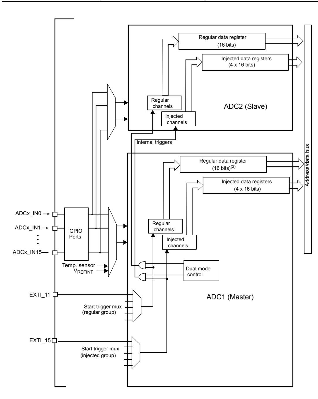
The diagram illustrates the internal architecture of a dual ADC system. On the left, various input sources are shown: ADCx_IN0 through ADCx_IN15 connected to GPIO Ports, a Temp. sensor VREFINT, and external triggers EXTI_11 and EXTI_15. These inputs are multiplexed and fed into two ADC units: ADC1 (Master) and ADC2 (Slave). ADC1 contains its own start trigger multiplexers for regular and injected groups. Both ADCs have 'Regular channels' and 'Injected channels' blocks. ADC1's regular channels output to a 'Regular data register (16 bits) (2) ', and its injected channels output to 'Injected data registers (4 x 16 bits)'. ADC2's regular channels output to a 'Regular data register (16 bits)', and its injected channels output to 'Injected data registers (4 x 16 bits)'. All data registers are connected to a common 'Address/data bus' on the right. A 'Dual mode control' block is connected to the start trigger multiplexers of both ADCs. A 'Temp. sensor VREFINT' input is also shown.
- 1. External triggers are present on ADC2 but are not shown for the purposes of this diagram.
- 2. In some dual ADC modes, the ADC1 data register (ADC1_DR) contains both ADC1 and ADC2 regular converted data over the entire 32 bits.
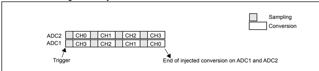
11.9.1 Injected simultaneous mode
This mode converts an injected channel group. The source of external trigger comes from the injected group mux of ADC1 (selected by the JEXTSEL[2:0] bits in the ADC1_CR2 register). A simultaneous trigger is provided to ADC2.
Note: Do not convert the same channel on the two ADCs (no overlapping sampling times for the two ADCs when converting the same channel).
At the end of conversion event on ADC1 or ADC2:
- • The converted data is stored in the ADC_JDRx registers of each ADC interface.
- • An JEOC interrupt is generated (if enabled on one of the two ADC interfaces) when the ADC1/ADC2 injected channels are all converted.
Note: In simultaneous mode, exactly the same sampling time should be configured for the two channels that will be sampled simultaneously by ACD1 and ADC2.
Figure 30. Injected simultaneous mode on 4 channels
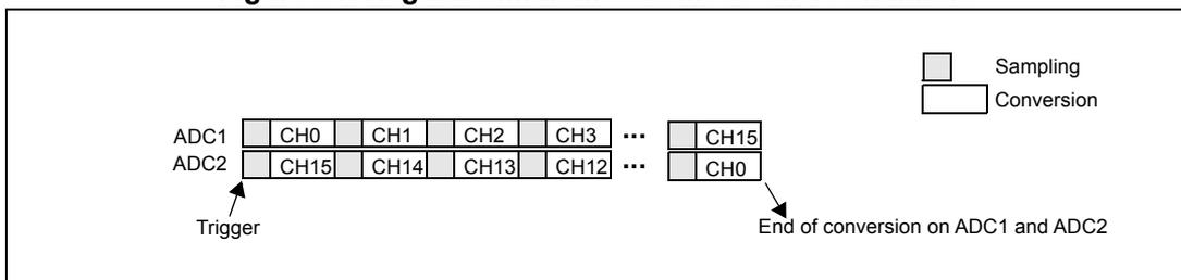
11.9.2 Regular simultaneous mode
This mode is performed on a regular channel group. The source of the external trigger comes from the regular group mux of ADC1 (selected by the EXTSEL[2:0] bits in the ADC1_CR2 register). A simultaneous trigger is provided to the ADC2.
Note: Do not convert the same channel on the two ADCs (no overlapping sampling times for the two ADCs when converting the same channel).
At the end of conversion event on ADC1 or ADC2:
- • A 32-bit DMA transfer request is generated (if DMA bit is set) which transfers to SRAM the ADC1_DR 32-bit register containing the ADC2 converted data in the upper halfword and the ADC1 converted data in the lower halfword.
- • An EOC interrupt is generated (if enabled on one of the two ADC interfaces) when ADC1/ADC2 regular channels are all converted.
Note: In regular simultaneous mode, exactly the same sampling time should be configured for the two channels that will be sampled simultaneously by ACD1 and ADC2.
Figure 31. Regular simultaneous mode on 16 channels
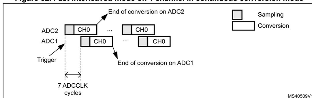
11.9.3 Fast interleaved mode
This mode can be started only on a regular channel group (usually one channel). The source of external trigger comes from the regular channel mux of ADC1. After an external trigger occurs:
- • ADC2 starts immediately and
- • ADC1 starts after a delay of 7 ADC clock cycles.
If CONT bit is set on both ADC1 and ADC2 the selected regular channels of both ADCs are continuously converted.
After an EOC interrupt is generated by ADC1 (if enabled through the EOCIE bit) a 32-bit DMA transfer request is generated (if the DMA bit is set) which transfers to SRAM the ADC1_DR 32-bit register containing the ADC2 converted data in the upper halfword and the ADC1 converted data in the lower half-word.
Note: The maximum sampling time allowed is <7 ADCCLK cycles to avoid the overlap between ADC1 and ADC2 sampling phases in the event that they convert the same channel.
Figure 32. Fast interleaved mode on 1 channel in continuous conversion mode
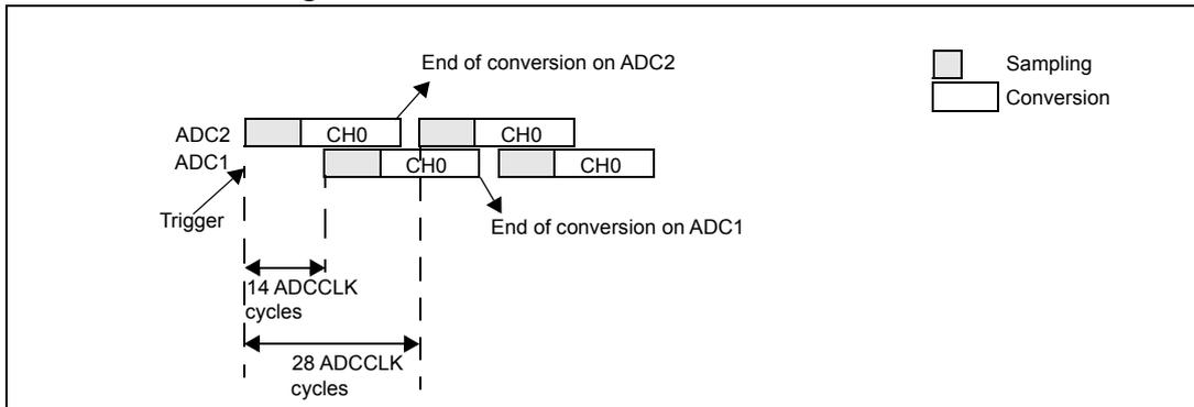
11.9.4 Slow interleaved mode
This mode can be started only on a regular channel group (only one channel). The source of external trigger comes from regular channel mux of ADC1. After external trigger occurs:
- • ADC2 starts immediately and
- • ADC1 starts after a delay of 14 ADC clock cycles.
- • ADC2 starts after a second delay of 14 ADC cycles, and so on.
Note: The maximum sampling time allowed is <14 ADCCLK cycles to avoid an overlap with the next conversion.
After an EOC interrupt is generated by ADC1 (if enabled through the EOCIE bit) a 32-bit DMA transfer request is generated (if the DMA bit is set) which transfers to SRAM the ADC1_DR 32-bit register containing the ADC2 converted data in the upper halfword and the ADC1 converted data in the lower halfword.
A new ADC2 start is automatically generated after 28 ADC clock cycles
CONT bit can not be set in the mode since it continuously converts the selected regular channel.
Note: The application must ensure that no external trigger for injected channel occurs when interleaved mode is enabled.
Figure 33. Slow interleaved mode on 1 channel
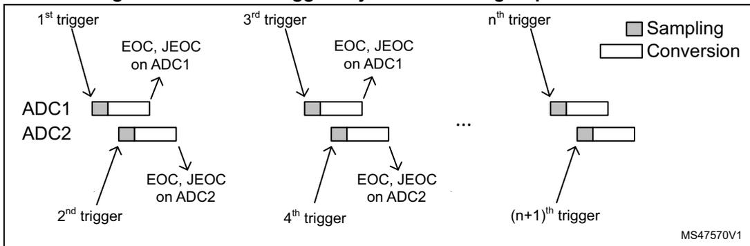
11.9.5 Alternate trigger mode
This mode can be started only on an injected channel group. The source of external trigger comes from the injected group mux of ADC1.
- • When the first trigger occurs, all injected group channels in ADC1 are converted.
- • When the second trigger arrives, all injected group channels in ADC2 are converted
- • and so on.
A JEOC interrupt, if enabled, is generated after all injected group channels of ADC1 are converted.
A JEOC interrupt, if enabled, is generated after all injected group channels of ADC2 are converted.
If another external trigger occurs after all injected group channels have been converted then the alternate trigger process restarts by converting ADC1 injected group channels.
Figure 34. Alternate trigger: injected channel group of each ADC
If the injected discontinuous mode is enabled for both ADC1 and ADC2:
- • When the first trigger occurs, the first injected channel in ADC1 is converted.
- • When the second trigger arrives, the first injected channel in ADC2 are converted
- • and so on....
A JEOC interrupt, if enabled, is generated after all injected group channels of ADC1 are converted.
A JEOC interrupt, if enabled, is generated after all injected group channels of ADC2 are converted.
If another external trigger occurs after all injected group channels have been converted then the alternate trigger process restarts.
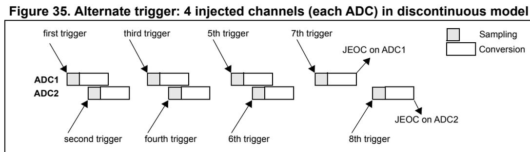
Figure 35. Alternate trigger: 4 injected channels (each ADC) in discontinuous model
11.9.6 Independent mode
In this mode the dual ADC synchronization is bypassed and each ADC interfaces works independently.
11.9.7 Combined regular/injected simultaneous mode
It is possible to interrupt simultaneous conversion of a regular group to start simultaneous conversion of an injected group.
Note: In combined regular/injected simultaneous mode, exactly the same sampling time should be configured for the two channels that will be sampled simultaneously by ADC1 and ADC2.
11.9.8 Combined regular simultaneous + alternate trigger mode
It is possible to interrupt regular group simultaneous conversion to start alternate trigger conversion of an injected group. Figure 36 shows the behavior of an alternate trigger interrupting a regular simultaneous conversion.
The injected alternate conversion is immediately started after the injected event arrives. If regular conversion is already running, in order to ensure synchronization after the injected conversion, the regular conversion of both (master/slave) ADCs is stopped and resumed synchronously at the end of the injected conversion.
Note: In combined regular simultaneous + alternate trigger mode, exactly the same sampling time should be configured for the two channels that will be sampled simultaneously by ADC1 and ADC2.
Figure 36. Alternate + Regular simultaneous
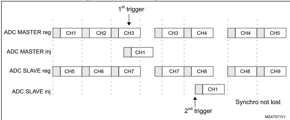
The diagram illustrates the timing of regular and injected conversions for master and slave ADCs:
- ADC MASTER reg: Shows regular conversions for CH1, CH2, CH3, CH3, CH4, CH4, and CH5.
- ADC MASTER inj: Shows an injected conversion for CH1 triggered by the 1st trigger.
- ADC SLAVE reg: Shows regular conversions for CH5, CH6, CH7, CH7, CH8, CH8, and CH9.
- ADC SLAVE inj: Shows an injected conversion for CH1 triggered by the 2nd trigger.
If a trigger occurs during an injected conversion that has interrupted a regular conversion, it will be ignored. Figure 37 shows the behavior in this case (the second trigger is ignored).
Figure 37. Case of trigger occurring during injected conversion
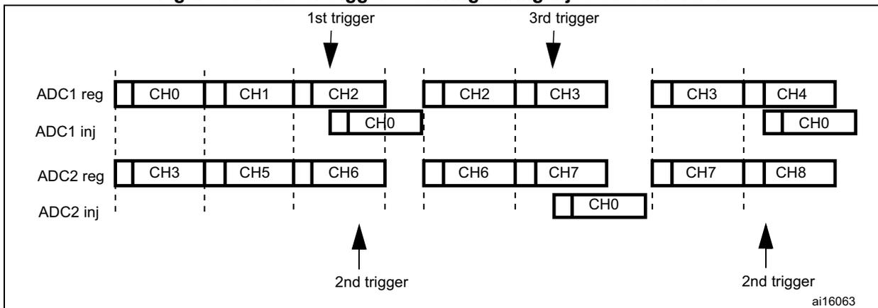
The diagram shows the effect of multiple triggers on ADC1 and ADC2:
- ADC1 reg: Regular conversions for CH0, CH1, CH2, CH2, CH3, CH3, and CH4.
- ADC1 inj: Injected conversions for CH0 triggered by the 1st and 3rd triggers.
- ADC2 reg: Regular conversions for CH3, CH5, CH6, CH6, CH7, CH7, and CH8.
- ADC2 inj: Injected conversion for CH0 triggered by the 2nd trigger.
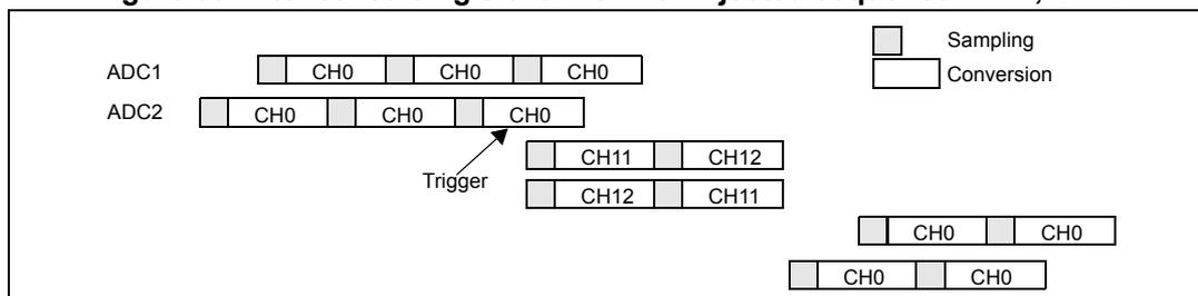
11.9.9 Combined injected simultaneous + interleaved
It is possible to interrupt an interleaved conversion with an injected event. In this case the interleaved conversion is interrupted and the injected conversion starts, at the end of the injected sequence the interleaved conversion is resumed. Figure 38 shows the behavior using an example.
Note: When the ADC clock prescaler is set to 4, the interleaved mode does not recover with evenly spaced sampling periods: the sampling interval is 8 ADC clock periods followed by 6 ADC clock periods, instead of 7 clock periods followed by 7 clock periods.
Figure 38. Interleaved single channel with injected sequence CH11, CH12
11.10 Temperature sensor
The temperature sensor can be used to measure the junction temperature ( \( T_J \) ) of the device.
The temperature sensor is internally connected to the \( ADCx\_IN16 \) input channel which is used to convert the sensor output voltage into a digital value. The recommended sampling time for the temperature sensor is 17.1 \( \mu\text{s} \) .
The block diagram of the temperature sensor is shown in Figure 39 .
When not in use, this sensor can be put in power down mode.
Note: The TSVREFE bit must be set to enable both internal channels: \( ADCx\_IN16 \) (temperature sensor) and \( ADCx\_IN17 \) ( \( V_{REFINT} \) ) conversion.
The temperature sensor output voltage changes linearly with temperature. The offset of this line varies from chip to chip due to process variations (up to 45 \( ^{\circ}\text{C} \) from one chip to another).
The internal temperature sensor is more suited to applications that detect temperature variations instead of absolute temperatures. If accurate temperature readings are needed, an external temperature sensor part should be used.
Figure 39. Temperature sensor and\( V_{REFINT} \) channel block diagram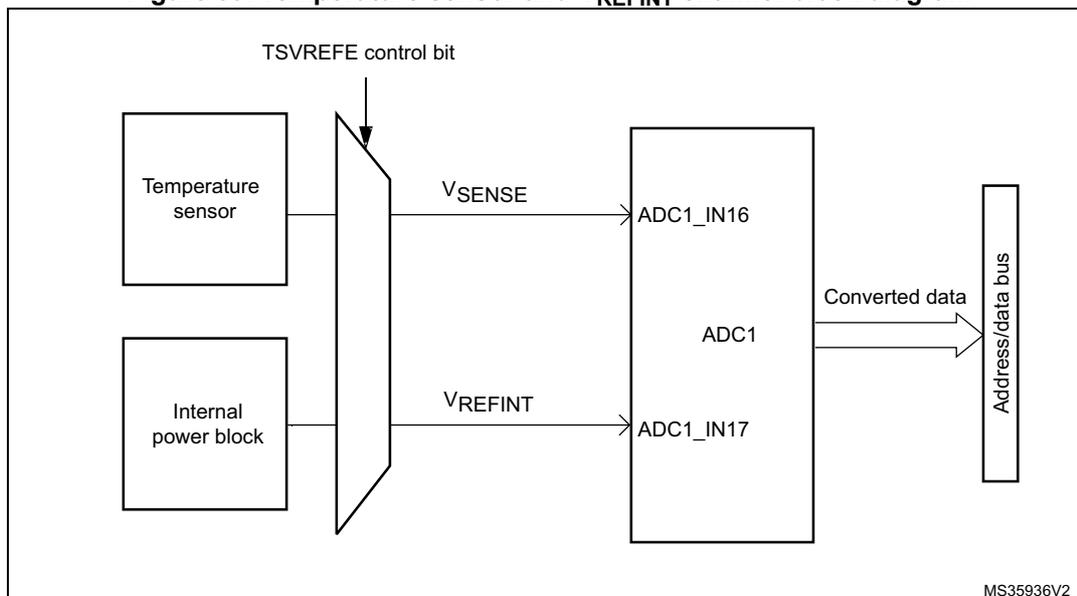
Reading the temperature
To use the sensor:
- 1. Select the ADCx_IN16 input channel.
- 2. Select a sample time of 17.1 \( \mu\text{s} \)
- 3. Set the TSVREFE bit in the ADC control register 2 (ADC_CR2) to wake up the temperature sensor from power down mode.
- 4. Start the ADC conversion by setting the ADON bit (or by external trigger).
- 5. Read the resulting \( V_{\text{SENSE}} \) data in the ADC data register
- 6. Obtain the temperature using the following formula:
Where,
\( V_{25} = V_{\text{SENSE}} \) value for \( 25^\circ\text{C} \) and
\( \text{Avg\_Slope} = \text{Average Slope for curve between Temperature vs. } V_{\text{SENSE}} \) (given in \( \text{mV}/^\circ\text{C} \) or \( \mu\text{V}/^\circ\text{C} \) ).
Refer to the Electrical characteristics section for the actual values of \( V_{25} \) and \( \text{Avg\_Slope} \) .
Note: The sensor has a startup time after waking from power down mode before it can output \( V_{\text{SENSE}} \) at the correct level. The ADC also has a startup time after power-on, so to minimize the delay, the ADON and TSVREFE bits should be set at the same time.
11.11 ADC interrupts
An interrupt can be produced on end of conversion for regular and injected groups and when the analog watchdog status bit is set. Separate interrupt enable bits are available for flexibility.
Note: ADC1 and ADC2 interrupts are mapped onto the same interrupt vector. ADC3 interrupts are mapped onto a separate interrupt vector.
Two other flags are present in the ADC_SR register, but there is no interrupt associated with them:
- • JSTRT (Start of conversion for injected group channels)
- • STRT (Start of conversion for regular group channels)
Table 71. ADC interrupts
| Interrupt event | Event flag | Enable Control bit |
|---|---|---|
| End of conversion regular group | EOC | EOCIE |
| End of conversion injected group | JEOC | JEOCIE |
| Analog watchdog status bit is set | AWD | AWDIE |
11.12 ADC registers
Refer to Section 2.2 on page 45 for a list of abbreviations used in register descriptions.
The peripheral registers have to be accessed by words (32-bit).
11.12.1 ADC status register (ADC_SR)
Address offset: 0x00
Reset value: 0x0000 0000
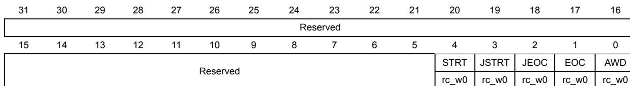
| 31 | 30 | 29 | 28 | 27 | 26 | 25 | 24 | 23 | 22 | 21 | 20 | 19 | 18 | 17 | 16 |
| Reserved | |||||||||||||||
| 15 | 14 | 13 | 12 | 11 | 10 | 9 | 8 | 7 | 6 | 5 | 4 | 3 | 2 | 1 | 0 |
| Reserved | STRT | JSTRT | JEOC | EOC | AWD | ||||||||||
| rc_w0 | rc_w0 | rc_w0 | rc_w0 | rc_w0 | |||||||||||
Bits 31:5 Reserved, must be kept at reset value.
Bit 4 STRT : Regular channel Start flag
This bit is set by hardware when regular channel conversion starts. It is cleared by software.
0: No regular channel conversion started
1: Regular channel conversion has started
Bit 3 JSTRT : Injected channel Start flag
This bit is set by hardware when injected channel group conversion starts. It is cleared by software.
0: No injected group conversion started
1: Injected group conversion has started
Bit 2 JEOC : Injected channel end of conversion
This bit is set by hardware at the end of all injected group channel conversion. It is cleared by software.
0: Conversion is not complete
1: Conversion complete
Bit 1 EOC : End of conversion
This bit is set by hardware at the end of a group channel conversion (regular or injected). It is cleared by software or by reading the ADC_DR.
0: Conversion is not complete
1: Conversion complete
Bit 0 AWD : Analog watchdog flag
This bit is set by hardware when the converted voltage crosses the values programmed in the ADC_LTR and ADC_HTR registers. It is cleared by software.
0: No Analog watchdog event occurred
1: Analog watchdog event occurred
11.12.2 ADC control register 1 (ADC_CR1)
Address offset: 0x04
Reset value: 0x0000 0000
| 31 | 30 | 29 | 28 | 27 | 26 | 25 | 24 | 23 | 22 | 21 | 20 | 19 | 18 | 17 | 16 |
|---|---|---|---|---|---|---|---|---|---|---|---|---|---|---|---|
| Reserved | AWDEN | JAWDEN | Reserved | DUALMOD[3:0] | |||||||||||
| rw | rw | rw | rw | rw | rw | ||||||||||
| 15 | 14 | 13 | 12 | 11 | 10 | 9 | 8 | 7 | 6 | 5 | 4 | 3 | 2 | 1 | 0 |
| DISCNUM[2:0] | JDISCE N | DISC EN | JAUTO | AWD SGL | SCAN | JEOC IE | AWDIE | EOCIE | AWDCH[4:0] | ||||||
| rw | rw | rw | rw | rw | rw | rw | rw | rw | rw | rw | rw | rw | rw | rw | rw |
Bits 31:24 Reserved, must be kept at reset value.
Bit 23 AWDEN : Analog watchdog enable on regular channels
This bit is set/reset by software.
0: Analog watchdog disabled on regular channels
1: Analog watchdog enabled on regular channels
Bit 22 JAWDEN : Analog watchdog enable on injected channels
This bit is set/reset by software.
0: Analog watchdog disabled on injected channels
1: Analog watchdog enabled on injected channels
Bits 21:20 Reserved, must be kept at reset value.
Bits 19:16 DUALMOD[3:0] : Dual mode selection
These bits are written by software to select the operating mode.
0000: Independent mode.
0001: Combined regular simultaneous + injected simultaneous mode
0010: Combined regular simultaneous + alternate trigger mode
0011: Combined injected simultaneous + fast interleaved mode
0100: Combined injected simultaneous + slow interleaved mode
0101: Injected simultaneous mode only
0110: Regular simultaneous mode only
0111: Fast interleaved mode only
1000: Slow interleaved mode only
1001: Alternate trigger mode only
Note: These bits are reserved in ADC2 and ADC3.
In dual mode, a change of channel configuration generates a restart that can produce a loss of synchronization. It is recommended to disable dual mode before any configuration change.
Bits 15:13 DISCNUM[2:0] : Discontinuous mode channel count
These bits are written by software to define the number of regular channels to be converted in discontinuous mode, after receiving an external trigger.
000: 1 channel
001: 2 channels
.....
111: 8 channels
Bit 12 JDISCEN: Discontinuous mode on injected channelsThis bit set and cleared by software to enable/disable discontinuous mode on injected group channels
0: Discontinuous mode on injected channels disabled
1: Discontinuous mode on injected channels enabled
Bit 11 DISCEN: Discontinuous mode on regular channelsThis bit set and cleared by software to enable/disable Discontinuous mode on regular channels.
0: Discontinuous mode on regular channels disabled
1: Discontinuous mode on regular channels enabled
Bit 10 JAUTO: Automatic Injected Group conversionThis bit set and cleared by software to enable/disable automatic injected group conversion after regular group conversion.
0: Automatic injected group conversion disabled
1: Automatic injected group conversion enabled
Bit 9 AWDSGL: Enable the watchdog on a single channel in scan modeThis bit set and cleared by software to enable/disable the analog watchdog on the channel identified by the AWDCH[4:0] bits.
0: Analog watchdog enabled on all channels
1: Analog watchdog enabled on a single channel
Bit 8 SCAN: Scan modeThis bit is set and cleared by software to enable/disable Scan mode. In Scan mode, the inputs selected through the ADC_SQRx or ADC_JSQRx registers are converted.
0: Scan mode disabled
1: Scan mode enabled
Note: An EOC or JEOC interrupt is generated only on the end of conversion of the last channel if the corresponding EOCIE or JEOCIE bit is set
Bit 7 JEOCIE: Interrupt enable for injected channelsThis bit is set and cleared by software to enable/disable the end of conversion interrupt for injected channels.
0: JEOC interrupt disabled
1: JEOC interrupt enabled. An interrupt is generated when the JEOC bit is set.
Bit 6 AWDIE : Analog watchdog interrupt enable
This bit is set and cleared by software to enable/disable the analog watchdog interrupt.
0: Analog watchdog interrupt disabled
1: Analog watchdog interrupt enabled
Bit 5 EOCIE : Interrupt enable for EOC
This bit is set and cleared by software to enable/disable the End of Conversion interrupt.
0: EOC interrupt disabled
1: EOC interrupt enabled. An interrupt is generated when the EOC bit is set.
Bits 4:0 AWDCH[4:0] : Analog watchdog channel select bits
These bits are set and cleared by software. They select the input channel to be guarded by the Analog watchdog.
00000: ADC analog Channel0
00001: ADC analog Channel1
...
01111: ADC analog Channel15
10000: ADC analog Channel16
10001: ADC analog Channel17
Other values: reserved.
Note: ADC1 analog Channel16 and Channel17 are internally connected to the temperature sensor and to V REFINT , respectively.
ADC2 analog inputs Channel16 and Channel17 are internally connected to V SS .
ADC3 analog inputs Channel9, Channel14, Channel15, Channel16 and Channel17 are connected to V SS .
11.12.3 ADC control register 2 (ADC_CR2)
Address offset: 0x08
Reset value: 0x0000 0000
| 31 | 30 | 29 | 28 | 27 | 26 | 25 | 24 | 23 | 22 | 21 | 20 | 19 | 18 | 17 | 16 |
|---|---|---|---|---|---|---|---|---|---|---|---|---|---|---|---|
| Reserved | TSVREFE | SWSTART | JSWSTART | EXTTRIG | EXTSEL[2:0] | Res. | |||||||||
| rw | rw | rw | rw | rw | rw | rw | |||||||||
| 15 | 14 | 13 | 12 | 11 | 10 | 9 | 8 | 7 | 6 | 5 | 4 | 3 | 2 | 1 | 0 |
| JEXTTRIG | JEXTSEL[2:0] | ALIGN | Reserved | DMA | Reserved | RSTCAL | CAL | CONT | ADON | ||||||
| rw | rw | rw | rw | rw | Res. | rw | rw | rw | rw | rw | |||||
Bits 31:24 Reserved, must be kept at reset value.
Bit 23 TSVREFE : Temperature sensor and \( V_{REFINT} \) enable
This bit is set and cleared by software to enable/disable the temperature sensor and \( V_{REFINT} \) channel. In devices with dual ADCs this bit is present only in ADC1.
0: Temperature sensor and \( V_{REFINT} \) channel disabled
1: Temperature sensor and \( V_{REFINT} \) channel enabled
Bit 22 SWSTART : Start conversion of regular channels
This bit is set by software to start conversion and cleared by hardware as soon as conversion starts. It starts a conversion of a group of regular channels if SWSTART is selected as trigger event by the EXTSEL[2:0] bits.
0: Reset state
1: Starts conversion of regular channels
Bit 21 JSWSTART : Start conversion of injected channels
This bit is set by software and cleared by software or by hardware as soon as the conversion starts. It starts a conversion of a group of injected channels (if JSWSTART is selected as trigger event by the JEXTSEL[2:0] bits).
0: Reset state
1: Starts conversion of injected channels
Bit 20 EXTTRIG : External trigger conversion mode for regular channels
This bit is set and cleared by software to enable/disable the external trigger used to start conversion of a regular channel group.
0: Conversion on external event disabled
1: Conversion on external event enabled
Bits 19:17 EXTSEL[2:0] : External event select for regular group
These bits select the external event used to trigger the start of conversion of a regular group:
For ADC1 and ADC2, the assigned triggers are:
000: Timer 1 CC1 event
001: Timer 1 CC2 event
010: Timer 1 CC3 event
011: Timer 2 CC2 event
100: Timer 3 TRGO event
101: Timer 4 CC4 event
110: EXTI line 11/TIM8_TRGO event (TIM8_TRGO is available only in high-density and XL-density devices)
111: SWSTART
For ADC3, the assigned triggers are:
000: Timer 3 CC1 event
001: Timer 2 CC3 event
010: Timer 1 CC3 event
011: Timer 8 CC1 event
100: Timer 8 TRGO event
101: Timer 5 CC1 event
110: Timer 5 CC3 event
111: SWSTART
Bit 16 Reserved, must be kept at reset value.
Bit 15 JEXTTRIG : External trigger conversion mode for injected channels
This bit is set and cleared by software to enable/disable the external trigger used to start conversion of an injected channel group.
0: Conversion on external event disabled
1: Conversion on external event enabled
Bits 14:12 JEXTSEL[2:0] : External event select for injected group
These bits select the external event used to trigger the start of conversion of an injected group:
For ADC1 and ADC2 the assigned triggers are:
000: Timer 1 TRGO event
001: Timer 1 CC4 event
010: Timer 2 TRGO event
011: Timer 2 CC1 event
100: Timer 3 CC4 event
101: Timer 4 TRGO event
110: EXTI line15/TIM8_CC4 event (TIM8_CC4 is available only in high-density and XL-density devices)
111: JSWSTART
For ADC3 the assigned triggers are:
000: Timer 1 TRGO event
001: Timer 1 CC4 event
010: Timer 4 CC3 event
011: Timer 8 CC2 event
100: Timer 8 CC4 event
101: Timer 5 TRGO event
110: Timer 5 CC4 event
111: JSWSTART
Bit 11 ALIGN : Data alignment
This bit is set and cleared by software. Refer to Figure 27 and Figure 28 .
0: Right Alignment
1: Left Alignment
Bits 10:9 Reserved, must be kept at reset value.
Bit 8 DMA : Direct memory access mode
This bit is set and cleared by software. Refer to the DMA controller chapter for more details.
0: DMA mode disabled
1: DMA mode enabled
Only ADC1 and ADC3 can generate a DMA request.
Bits 7:4 Reserved, must be kept at reset value.
Bit 3 RSTCAL : Reset calibration
This bit is set by software and cleared by hardware. It is cleared after the calibration registers are initialized.
0: Calibration register initialized.
1: Initialize calibration register.
Note: If RSTCAL is set when conversion is ongoing, additional cycles are required to clear the calibration registers.
Bit 2 CAL : A/D CalibrationThis bit is set by software to start the calibration. It is reset by hardware after calibration is complete.
0: Calibration completed
1: Enable calibration
This bit is set and cleared by software. If set conversion takes place continuously till this bit is reset.
0: Single conversion mode
1: Continuous conversion mode
This bit is set and cleared by software. If this bit holds a value of zero and a 1 is written to it then it wakes up the ADC from Power Down state.
Conversion starts when this bit holds a value of 1 and a 1 is written to it. The application should allow a delay of \( t_{STAB} \) between power up and start of conversion. Refer to Figure 23 .
0: Disable ADC conversion/calibration and go to power down mode.
1: Enable ADC and to start conversion
Note: If any other bit in this register apart from ADON is changed at the same time, then conversion is not triggered. This is to prevent triggering an erroneous conversion.
11.12.4 ADC sample time register 1 (ADC_SMPR1)
Address offset: 0x0C
Reset value: 0x0000 0000
| 31 | 30 | 29 | 28 | 27 | 26 | 25 | 24 | 23 | 22 | 21 | 20 | 19 | 18 | 17 | 16 |
|---|---|---|---|---|---|---|---|---|---|---|---|---|---|---|---|
| Reserved | SMP17[2:0] | SMP16[2:0] | SMP15[2:1] | ||||||||||||
| rw | rw | rw | rw | rw | rw | rw | rw | ||||||||
| 15 | 14 | 13 | 12 | 11 | 10 | 9 | 8 | 7 | 6 | 5 | 4 | 3 | 2 | 1 | 0 |
| SMP15_0 | SMP14[2:0] | SMP13[2:0] | SMP12[2:0] | SMP11[2:0] | SMP10[2:0] | ||||||||||
| rw | rw | rw | rw | rw | rw | rw | rw | rw | rw | rw | rw | rw | rw | rw | |
Bits 31:24 Reserved, must be kept at reset value.
Bits 23:0 SMPx[2:0] : Channel x Sample time selection
These bits are written by software to select the sample time individually for each channel. During sample cycles channel selection bits must remain unchanged.
- 000: 1.5 cycles
- 001: 7.5 cycles
- 010: 13.5 cycles
- 011: 28.5 cycles
- 100: 41.5 cycles
- 101: 55.5 cycles
- 110: 71.5 cycles
- 111: 239.5 cycles
Note: ADC1 analog Channel16 and Channel 17 are internally connected to the temperature sensor and to V
REFINT
, respectively.
ADC2 analog input Channel16 and Channel17 are internally connected to V
SS
.
ADC3 analog inputs Channel14, Channel15, Channel16 and Channel17 are connected to V
SS
.
11.12.5 ADC sample time register 2 (ADC_SMPR2)
Address offset: 0x10
Reset value: 0x0000 0000
| 31 | 30 | 29 | 28 | 27 | 26 | 25 | 24 | 23 | 22 | 21 | 20 | 19 | 18 | 17 | 16 |
|---|---|---|---|---|---|---|---|---|---|---|---|---|---|---|---|
| Reserved | SMP9[2:0] | SMP8[2:0] | SMP7[2:0] | SMP6[2:0] | SMP5[2:1] | ||||||||||
| Res. | rw | rw | rw | rw | rw | rw | rw | rw | rw | rw | rw | rw | rw | rw | rw |
| 15 | 14 | 13 | 12 | 11 | 10 | 9 | 8 | 7 | 6 | 5 | 4 | 3 | 2 | 1 | 0 |
| SMP5_0 | SMP4[2:0] | SMP3[2:0] | SMP2[2:0] | SMP1[2:0] | SMP0[2:0] | ||||||||||
| rw | rw | rw | rw | rw | rw | rw | rw | rw | rw | rw | rw | rw | rw | rw | rw |
Bits 31:30 Reserved, must be kept at reset value.
Bits 29:0 SMPx[2:0] : Channel x Sample time selection
These bits are written by software to select the sample time individually for each channel. During sample cycles channel selection bits must remain unchanged.
000: 1.5 cycles
001: 7.5 cycles
010: 13.5 cycles
011: 28.5 cycles
100: 41.5 cycles
101: 55.5 cycles
110: 71.5 cycles
111: 239.5 cycles
Note: ADC3 analog input Channel9 is connected to V SS .
11.12.6 ADC injected channel data offset register x (ADC_JOFRx) (x=1..4)
Address offset: 0x14-0x20
Reset value: 0x0000 0000
| 31 | 30 | 29 | 28 | 27 | 26 | 25 | 24 | 23 | 22 | 21 | 20 | 19 | 18 | 17 | 16 |
|---|---|---|---|---|---|---|---|---|---|---|---|---|---|---|---|
| Reserved | |||||||||||||||
| 15 | 14 | 13 | 12 | 11 | 10 | 9 | 8 | 7 | 6 | 5 | 4 | 3 | 2 | 1 | 0 |
| Reserved | JOFFSETx[11:0] | ||||||||||||||
| rw | rw | rw | rw | rw | rw | rw | rw | rw | rw | rw | |||||
Bits 31:12 Reserved, must be kept at reset value.
Bits 11:0 JOFFSETx[11:0] : Data offset for injected channel x
These bits are written by software to define the offset to be subtracted from the raw converted data when converting injected channels. The conversion result can be read from in the ADC_JDRx registers.
11.12.7 ADC watchdog high threshold register (ADC_HTR)
Address offset: 0x24
Reset value: 0x0000 0FFF
| 31 | 30 | 29 | 28 | 27 | 26 | 25 | 24 | 23 | 22 | 21 | 20 | 19 | 18 | 17 | 16 |
|---|---|---|---|---|---|---|---|---|---|---|---|---|---|---|---|
| Reserved | |||||||||||||||
| 15 | 14 | 13 | 12 | 11 | 10 | 9 | 8 | 7 | 6 | 5 | 4 | 3 | 2 | 1 | 0 |
| Reserved | HT[11:0] | ||||||||||||||
| rw | rw | rw | rw | rw | rw | rw | rw | rw | rw | rw | rw | ||||
Bits 31:12 Reserved, must be kept at reset value.
Bits 11:0 HT[11:0] : Analog watchdog high threshold
These bits are written by software to define the high threshold for the analog watchdog.
Note: The software can write to these registers when an ADC conversion is ongoing. The programmed value will be effective when the next conversion is complete. Writing to this register is performed with a write delay that can create uncertainty on the effective time at which the new value is programmed.
11.12.8 ADC watchdog low threshold register (ADC_LTR)
Address offset: 0x28
Reset value: 0x0000 0000
| 31 | 30 | 29 | 28 | 27 | 26 | 25 | 24 | 23 | 22 | 21 | 20 | 19 | 18 | 17 | 16 |
|---|---|---|---|---|---|---|---|---|---|---|---|---|---|---|---|
| Reserved | |||||||||||||||
| 15 | 14 | 13 | 12 | 11 | 10 | 9 | 8 | 7 | 6 | 5 | 4 | 3 | 2 | 1 | 0 |
| Reserved | LT[11:0] | ||||||||||||||
| rw | rw | rw | rw | rw | rw | rw | rw | rw | rw | rw | rw | ||||
Bits 31:12 Reserved, must be kept at reset value.
Bits 11:0 LT[11:0] : Analog watchdog low threshold
These bits are written by software to define the low threshold for the analog watchdog.
Note: The software can write to these registers when an ADC conversion is ongoing. The programmed value will be effective when the next conversion is complete. Writing to this register is performed with a write delay that can create uncertainty on the effective time at which the new value is programmed.
11.12.9 ADC regular sequence register 1 (ADC_SQR1)
Address offset: 0x2C
Reset value: 0x0000 0000
| 31 | 30 | 29 | 28 | 27 | 26 | 25 | 24 | 23 | 22 | 21 | 20 | 19 | 18 | 17 | 16 |
|---|---|---|---|---|---|---|---|---|---|---|---|---|---|---|---|
| Reserved | L[3:0] | SQ16[4:1] | |||||||||||||
| rw | rw | rw | rw | rw | rw | rw | rw | ||||||||
| 15 | 14 | 13 | 12 | 11 | 10 | 9 | 8 | 7 | 6 | 5 | 4 | 3 | 2 | 1 | 0 |
| SQ16_0 | SQ15[4:0] | SQ14[4:0] | SQ13[4:0] | ||||||||||||
| rw | rw | rw | rw | rw | rw | rw | rw | rw | rw | rw | rw | rw | rw | rw | rw |
Bits 31:24 Reserved, must be kept at reset value.
Bits 23:20 L[3:0] : Regular channel sequence length
These bits are written by software to define the total number of conversions in the regular channel conversion sequence.
0000: 1 conversion
0001: 2 conversions
.....
1111: 16 conversions
Bits 19:15 SQ16[4:0] : 16th conversion in regular sequence
These bits are written by software with the channel number (0..17) assigned as the 16th in the conversion sequence.
Bits 14:10 SQ15[4:0] : 15th conversion in regular sequence
Bits 9:5 SQ14[4:0] : 14th conversion in regular sequence
Bits 4:0 SQ13[4:0] : 13th conversion in regular sequence
11.12.10 ADC regular sequence register 2 (ADC_SQR2)
Address offset: 0x30
Reset value: 0x0000 0000
| 31 | 30 | 29 | 28 | 27 | 26 | 25 | 24 | 23 | 22 | 21 | 20 | 19 | 18 | 17 | 16 |
|---|---|---|---|---|---|---|---|---|---|---|---|---|---|---|---|
| Reserved | SQ12[4:0] | SQ11[4:0] | SQ10[4:1] | ||||||||||||
| rw | rw | rw | rw | rw | rw | rw | rw | rw | rw | rw | rw | rw | rw | rw | |
| 15 | 14 | 13 | 12 | 11 | 10 | 9 | 8 | 7 | 6 | 5 | 4 | 3 | 2 | 1 | 0 |
| SQ10_0 | SQ9[4:0] | SQ8[4:0] | SQ7[4:0] | ||||||||||||
| rw | rw | rw | rw | rw | rw | rw | rw | rw | rw | rw | rw | rw | rw | rw | |
Bits 31:30 Reserved, must be kept at reset value.
Bits 29:26 SQ12[4:0] : 12th conversion in regular sequence
These bits are written by software with the channel number (0..17) assigned as the 12th in the sequence to be converted.
Bits 24:20 SQ11[4:0] : 11th conversion in regular sequence
Bits 19:15 SQ10[4:0] : 10th conversion in regular sequence
Bits 14:10 SQ9[4:0] : 9th conversion in regular sequence
Bits 9:5 SQ8[4:0] : 8th conversion in regular sequence
Bits 4:0 SQ7[4:0] : 7th conversion in regular sequence
11.12.11 ADC regular sequence register 3 (ADC_SQR3)
Address offset: 0x34
Reset value: 0x0000 0000
| 31 | 30 | 29 | 28 | 27 | 26 | 25 | 24 | 23 | 22 | 21 | 20 | 19 | 18 | 17 | 16 |
|---|---|---|---|---|---|---|---|---|---|---|---|---|---|---|---|
| Reserved | SQ6[4:0] | SQ5[4:0] | SQ4[4:1] | ||||||||||||
| rw | rw | rw | rw | rw | rw | rw | rw | rw | rw | rw | rw | rw | rw | rw | |
| 15 | 14 | 13 | 12 | 11 | 10 | 9 | 8 | 7 | 6 | 5 | 4 | 3 | 2 | 1 | 0 |
| SQ4_0 | SQ3[4:0] | SQ2[4:0] | SQ1[4:0] | ||||||||||||
| rw | rw | rw | rw | rw | rw | rw | rw | rw | rw | rw | rw | rw | rw | rw | rw |
Bits 31:30 Reserved, must be kept at reset value.
Bits 29:25 SQ6[4:0] : 6th conversion in regular sequence
These bits are written by software with the channel number (0..17) assigned as the 6th in the sequence to be converted.
Bits 24:20 SQ5[4:0] : 5th conversion in regular sequence
Bits 19:15 SQ4[4:0] : fourth conversion in regular sequence
Bits 14:10 SQ3[4:0] : third conversion in regular sequence
Bits 9:5 SQ2[4:0] : second conversion in regular sequence
Bits 4:0 SQ1[4:0] : first conversion in regular sequence
11.12.12 ADC injected sequence register (ADC_JSQR)
Address offset: 0x38
Reset value: 0x0000 0000
| 31 | 30 | 29 | 28 | 27 | 26 | 25 | 24 | 23 | 22 | 21 | 20 | 19 | 18 | 17 | 16 |
|---|---|---|---|---|---|---|---|---|---|---|---|---|---|---|---|
| Reserved | JL[1:0] | JSQ4[4:1] | |||||||||||||
| rw | rw | rw | rw | rw | rw | ||||||||||
| 15 | 14 | 13 | 12 | 11 | 10 | 9 | 8 | 7 | 6 | 5 | 4 | 3 | 2 | 1 | 0 |
| JSQ4_0 | JSQ3[4:0] | JSQ2[4:0] | JSQ1[4:0] | ||||||||||||
| rw | rw | rw | rw | rw | rw | rw | rw | rw | rw | rw | rw | rw | rw | rw | rw |
Bits 31:22 Reserved, must be kept at reset value.
Bits 21:20 JL[1:0] : Injected sequence length
These bits are written by software to define the total number of conversions in the injected channel conversion sequence.
- 00: 1 conversion
- 01: 2 conversions
- 10: 3 conversions
- 11: 4 conversions
Bits 19:15 JSQ4[4:0] : fourth conversion in injected sequence (when JL[1:0] = 3) (1)
These bits are written by software with the channel number (0..17) assigned as the fourth in the sequence to be converted.
Note: Unlike a regular conversion sequence, if JL[1:0] length is less than four, the channels are converted in a sequence starting from (4-JL). Example: ADC_JSQR[21:0] = 10 00011 00011 00111 00010 means that a scan conversion will convert the following channel sequence: 7, 3, 3, 3. (not 2, 7, 3)
Bits 14:10 JSQ3[4:0] : third conversion in injected sequence (when JL[1:0] = 3)
Bits 9:5 JSQ2[4:0] : second conversion in injected sequence (when JL[1:0] = 3)
Bits 4:0 JSQ1[4:0] : first conversion in injected sequence (when JL[1:0] = 3)
- 1. When JL=3 ( 4 injected conversions in the sequencer), the ADC converts the channels in this order:
JSQ1[4:0] >> JSQ2[4:0] >> JSQ3[4:0] >> JSQ4[4:0]
When JL=2 ( 3 injected conversions in the sequencer), the ADC converts the channels in this order:
JSQ2[4:0] >> JSQ3[4:0] >> JSQ4[4:0]
When JL=1 ( 2 injected conversions in the sequencer), the ADC converts the channels in this order:
JSQ3[4:0] >> JSQ4[4:0]
When JL=0 ( 1 injected conversion in the sequencer), the ADC converts only JSQ4[4:0] channel
11.12.13 ADC injected data register x (ADC_JDRx) (x= 1..4)
Address offset: 0x3C - 0x48
Reset value: 0x0000 0000
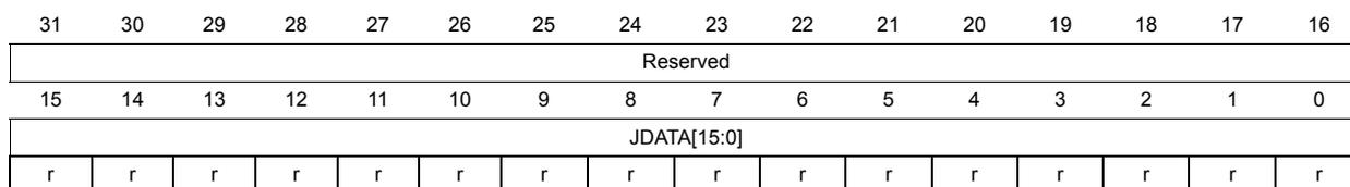
| 31 | 30 | 29 | 28 | 27 | 26 | 25 | 24 | 23 | 22 | 21 | 20 | 19 | 18 | 17 | 16 |
| Reserved | |||||||||||||||
| 15 | 14 | 13 | 12 | 11 | 10 | 9 | 8 | 7 | 6 | 5 | 4 | 3 | 2 | 1 | 0 |
| JDATA[15:0] | |||||||||||||||
| r | r | r | r | r | r | r | r | r | r | r | r | r | r | r | r |
Bits 31:16 Reserved, must be kept at reset value.
Bits 15:0 JDATA[15:0] : Injected data
These bits are read only. They contain the conversion result from injected channel x. The data is left or right-aligned as shown in Figure 27 and Figure 28 .
11.12.14 ADC regular data register (ADC_DR)
Address offset: 0x4C
Reset value: 0x0000 0000
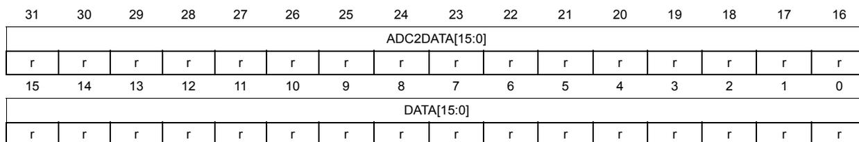
| 31 | 30 | 29 | 28 | 27 | 26 | 25 | 24 | 23 | 22 | 21 | 20 | 19 | 18 | 17 | 16 |
| ADC2DATA[15:0] | |||||||||||||||
| r | r | r | r | r | r | r | r | r | r | r | r | r | r | r | r |
| 15 | 14 | 13 | 12 | 11 | 10 | 9 | 8 | 7 | 6 | 5 | 4 | 3 | 2 | 1 | 0 |
| DATA[15:0] | |||||||||||||||
| r | r | r | r | r | r | r | r | r | r | r | r | r | r | r | r |
Bits 31:16 ADC2DATA[15:0] : ADC2 data
In ADC1: In dual mode, these bits contain the regular data of ADC2. Refer to Section 11.9: Dual ADC mode .
In ADC2 and ADC3: these bits are not used.
Bits 15:0 DATA[15:0] : Regular data
These bits are read only. They contain the conversion result from the regular channels. The data is left or right-aligned as shown in Figure 27 and Figure 28 .
11.12.15 ADC register map
The following table summarizes the ADC registers.
Table 72. ADC register map and reset values
| Offset | Register | 31 | 30 | 29 | 28 | 27 | 26 | 25 | 24 | 23 | 22 | 21 | 20 | 19 | 18 | 17 | 16 | 15 | 14 | 13 | 12 | 11 | 10 | 9 | 8 | 7 | 6 | 5 | 4 | 3 | 2 | 1 | 0 |
|---|---|---|---|---|---|---|---|---|---|---|---|---|---|---|---|---|---|---|---|---|---|---|---|---|---|---|---|---|---|---|---|---|---|
| 0x00 | ADC_SR | Reserved | STRT | JSRT | JEOD | EOC | AWD | ||||||||||||||||||||||||||
| Reset value | 0 | 0 | 0 | 0 | 0 | ||||||||||||||||||||||||||||
| 0x04 | ADC_CR1 | Reserved | AWDEN | JAWDEN | Reserved | DUALMOD [3:0] | DISCNUM [2:0] | JDISCEN | DISCEN | JAUTO | AWDSGL | SCAN | JEOCIEN | AWDIE | EOCIE | AWDCH[4:0] | |||||||||||||||||
| Reset value | 0 | 0 | 0 | 0 | 0 | 0 | 0 | 0 | 0 | 0 | 0 | 0 | 0 | 0 | 0 | ||||||||||||||||||
| 0x08 | ADC_CR2 | Reserved | TSVREFE | SWSTART | JSWSTART | EXTTRIG | EXTSEL [2:0] | Reserved | JEXTTRIG | JEXTSEL [2:0] | ALIGN | Reserved | DMA | Reserved | RSTCAL | CAL | CONT | ADON | Reserved | ||||||||||||||
| Reset value | 0 | 0 | 0 | 0 | 0 | 0 | 0 | 0 | 0 | 0 | 0 | 0 | 0 | 0 | 0 | ||||||||||||||||||
| 0x0C | ADC_SMPR1 | Sample time bits SMPx_x | |||||||||||||||||||||||||||||||
| Reset value | 0 | 0 | 0 | 0 | 0 | 0 | 0 | 0 | 0 | 0 | 0 | 0 | 0 | 0 | 0 | 0 | 0 | 0 | 0 | 0 | 0 | 0 | 0 | 0 | 0 | 0 | 0 | 0 | 0 | 0 | 0 | ||
| 0x10 | ADC_SMPR2 | Sample time bits SMPx_x | |||||||||||||||||||||||||||||||
| Reset value | 0 | 0 | 0 | 0 | 0 | 0 | 0 | 0 | 0 | 0 | 0 | 0 | 0 | 0 | 0 | 0 | 0 | 0 | 0 | 0 | 0 | 0 | 0 | 0 | 0 | 0 | 0 | 0 | 0 | 0 | 0 | ||
| 0x14 | ADC_JOFR1 | Reserved | |||||||||||||||||||||||||||||||
| Reset value | |||||||||||||||||||||||||||||||||
| 0x18 | ADC_JOFR2 | Reserved | |||||||||||||||||||||||||||||||
| Reset value | |||||||||||||||||||||||||||||||||
| 0x1C | ADC_JOFR3 | Reserved | |||||||||||||||||||||||||||||||
| Reset value | |||||||||||||||||||||||||||||||||
| 0x20 | ADC_JOFR4 | Reserved | |||||||||||||||||||||||||||||||
| Reset value | |||||||||||||||||||||||||||||||||
| 0x24 | ADC_HTR | Reserved | |||||||||||||||||||||||||||||||
| Reset value | |||||||||||||||||||||||||||||||||
| 0x28 | ADC_LTR | Reserved | |||||||||||||||||||||||||||||||
| Reset value | |||||||||||||||||||||||||||||||||
| 0x2C | ADC_SQR1 | Reserved | |||||||||||||||||||||||||||||||
| Reset value | |||||||||||||||||||||||||||||||||
Table 72. ADC register map and reset values (continued)
| Offset | Register | 31 | 30 | 29 | 28 | 27 | 26 | 25 | 24 | 23 | 22 | 21 | 20 | 19 | 18 | 17 | 16 | 15 | 14 | 13 | 12 | 11 | 10 | 9 | 8 | 7 | 6 | 5 | 4 | 3 | 2 | 1 | 0 |
|---|---|---|---|---|---|---|---|---|---|---|---|---|---|---|---|---|---|---|---|---|---|---|---|---|---|---|---|---|---|---|---|---|---|
| 0 | 0 | 0 | 0 | 0 | 0 | 0 | 0 | 0 | 0 | 0 | 0 | 0 | 0 | 0 | 0 | 0 | 0 | 0 | 0 | 0 | 0 | 0 | 0 | 0 | 0 | 0 | 0 | 0 | 0 | 0 | 0 | ||
| 0x30 | ADC_SQR2 | Reserved | SQ12[4:0] 12th conversion in regular sequence bits | SQ11[4:0] 11th conversion in regular sequence bits | SQ10[4:0] 10th conversion in regular sequence bits | SQ9[4:0] 9th conversion in regular sequence bits | SQ8[4:0] 8th conversion in regular sequence bits | SQ7[4:0] 7th conversion in regular sequence bits | |||||||||||||||||||||||||
| Reset value | 0 | 0 | 0 | 0 | 0 | 0 | 0 | 0 | 0 | 0 | 0 | 0 | 0 | 0 | 0 | 0 | 0 | 0 | 0 | 0 | 0 | 0 | 0 | 0 | 0 | 0 | 0 | 0 | 0 | 0 | |||
| 0x34 | ADC_SQR3 | Reserved | SQ6[4:0] 6th conversion in regular sequence bits | SQ5[4:0] 5th conversion in regular sequence bits | SQ4[4:0] fourth conversion in regular sequence bits | SQ3[4:0] third conversion in regular sequence bits | SQ2[4:0] second conversion in regular sequence bits | SQ1[4:0] first conversion in regular sequence bits | |||||||||||||||||||||||||
| Reset value | 0 | 0 | 0 | 0 | 0 | 0 | 0 | 0 | 0 | 0 | 0 | 0 | 0 | 0 | 0 | 0 | 0 | 0 | 0 | 0 | 0 | 0 | 0 | 0 | 0 | 0 | 0 | 0 | 0 | 0 | |||
| 0x38 | ADC_JSQR | Reserved | |||||||||||||||||||||||||||||||
| Reset value | |||||||||||||||||||||||||||||||||
| 0x3C | ADC_JDR1 | Reserved | |||||||||||||||||||||||||||||||
| Reset value | |||||||||||||||||||||||||||||||||
| 0x40 | ADC_JDR2 | Reserved | |||||||||||||||||||||||||||||||
| Reset value | |||||||||||||||||||||||||||||||||
| 0x44 | ADC_JDR3 | Reserved | |||||||||||||||||||||||||||||||
| Reset value | |||||||||||||||||||||||||||||||||
| 0x48 | ADC_JDR4 | Reserved | |||||||||||||||||||||||||||||||
| Reset value | |||||||||||||||||||||||||||||||||
| 0x4C | ADC_DR | ADC2DATA[15:0] | |||||||||||||||||||||||||||||||
| Reset value | |||||||||||||||||||||||||||||||||
Refer to Table 3 on page 50 for the register boundary addresses.