5. Power control (PWR)
Low-density devices are STM32F101xx, STM32F102xx and STM32F103xx microcontrollers where the Flash memory density ranges between 16 and 32 Kbytes.
Medium-density devices are STM32F101xx, STM32F102xx and STM32F103xx microcontrollers where the Flash memory density ranges between 64 and 128 Kbytes.
High-density devices are STM32F101xx and STM32F103xx microcontrollers where the Flash memory density ranges between 256 and 512 Kbytes.
XL-density devices are STM32F101xx and STM32F103xx microcontrollers where the Flash memory density ranges between 768 Kbytes and 1 Mbyte.
Connectivity line devices are STM32F105xx and STM32F107xx microcontrollers.
This section applies to the whole STM32F101xx family, unless otherwise specified.
5.1 Power supplies
The device requires a 2.0-to-3.6 V operating voltage supply ( \( V_{DD} \) ). An embedded regulator is used to supply the internal 1.8 V digital power.
The real-time clock (RTC) and backup registers can be powered from the \( V_{BAT} \) voltage when the main \( V_{DD} \) supply is powered off.
Figure 4. Power supply overview
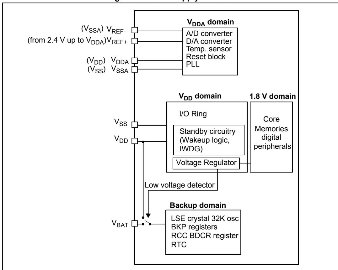
The diagram illustrates the power supply architecture of a microcontroller, organized into several functional domains and their connections to external pins:
- V DDA domain: Connected to pins (V SSA ) V REF- , (from 2.4 V up to V DDA ) V REF+ , (V DD ) V DDA , and (V SS ) V SSA . It contains the A/D converter, D/A converter, Temp. sensor, Reset block, and PLL.
- V DD domain: Connected to pins V SS and V DD . It contains the I/O Ring, Standby circuitry (Wakeup logic, IWDG), and a Voltage Regulator.
- 1.8 V domain: Connected to the Voltage Regulator. It contains Core Memories and digital peripherals.
- Backup domain: Connected to pin V BAT . It contains the LSE crystal 32K osc, BKP registers, RCC BDCR register, and RTC. This domain is also connected to a Low voltage detector.
1. V DDA and V SSA must be connected to V DD and V SS , respectively.
5.1.1 Independent A/D and D/A converter supply and reference voltage
To improve conversion accuracy, the ADC and the DAC have an independent power supply which can be separately filtered and shielded from noise on the PCB.
- • The ADC and DAC voltage supply input is available on a separate V DDA pin.
- • An isolated supply ground connection is provided on pin V SSA .
When available (according to package), V REF- must be tied to V SSA .
On 100-pin and 144-pin packages
To ensure a better accuracy on low-voltage inputs and outputs, the user can connect a separate external reference voltage on V REF+ . V REF+ is the highest voltage, represented by the full scale value, for an analog input (ADC) or output (DAC) signal. The voltage on V REF+ can range from 2.4 V to V DDA .
On 64-pin packages and packages with less pins
The V REF+ and V REF- pins are not available, they are internally connected to the ADC voltage supply (V DDA ) and ground (V SSA ).
5.1.2 Battery backup domain
To retain the content of the Backup registers and supply the RTC function when \( V_{DD} \) is turned off, \( V_{BAT} \) pin can be connected to an optional standby voltage supplied by a battery or by another source.
The \( V_{BAT} \) pin powers the RTC unit, the LSE oscillator and the PC13 to PC15 IOs, allowing the RTC to operate even when the main digital supply ( \( V_{DD} \) ) is turned off. The switch to the \( V_{BAT} \) supply is controlled by the Power Down Reset embedded in the Reset block.
Warning:
During
\(
t_{RSTTEMPO}
\)
(temporization at
\(
V_{DD}
\)
startup) or after a PDR is detected, the power switch between
\(
V_{BAT}
\)
and
\(
V_{DD}
\)
remains connected to
\(
V_{BAT}
\)
.
During the startup phase, if
\(
V_{DD}
\)
is established in less than
\(
t_{RSTTEMPO}
\)
(Refer to the datasheet for the value of
\(
t_{RSTTEMPO}
\)
) and
\(
V_{DD} > V_{BAT} + 0.6\text{ V}
\)
, a current may be injected into
\(
V_{BAT}
\)
through an internal diode connected between
\(
V_{DD}
\)
and the power switch (
\(
V_{BAT}
\)
).
If the power supply/battery connected to the
\(
V_{BAT}
\)
pin cannot support this current injection, it is strongly recommended to connect an external low-drop diode between this power supply and the
\(
V_{BAT}
\)
pin.
If no external battery is used in the application, it is recommended to connect \( V_{BAT} \) externally to \( V_{DD} \) with a 100 nF external ceramic decoupling capacitor (for more details refer to AN2586).
When the backup domain is supplied by \( V_{DD} \) (analog switch connected to \( V_{DD} \) ), the following functions are available:
- • PC14 and PC15 can be used as either GPIO or LSE pins
- • PC13 can be used as GPIO, TAMPER pin, RTC Calibration Clock, RTC Alarm or second output (refer to Section 6: Backup registers (BKP) )
Note: Due to the fact that the switch only sinks a limited amount of current (3 mA), the use of GPIOs PC13 to PC15 in output mode is restricted: the speed has to be limited to 2 MHz with a maximum load of 30 pF and these IOs must not be used as a current source (e.g. to drive a LED).
When the backup domain is supplied by \( V_{BAT} \) (analog switch connected to \( V_{BAT} \) because \( V_{DD} \) is not present), the following functions are available:
- • PC14 and PC15 can be used as LSE pins only
- • PC13 can be used as TAMPER pin, RTC Alarm or Second output (refer to Section 6.4.2: RTC clock calibration register (BKP_RTCCR) ).
5.1.3 Voltage regulator
The voltage regulator is always enabled after Reset. It works in three different modes depending on the application modes.
- • In Run mode, the regulator supplies full power to the 1.8 V domain (core, memories and digital peripherals).
- • In Stop mode the regulator supplies low-power to the 1.8 V domain, preserving contents of registers and SRAM
- • In Standby Mode, the regulator is powered off. The contents of the registers and SRAM are lost except for the Standby circuitry and the Backup Domain.
5.2 Power supply supervisor
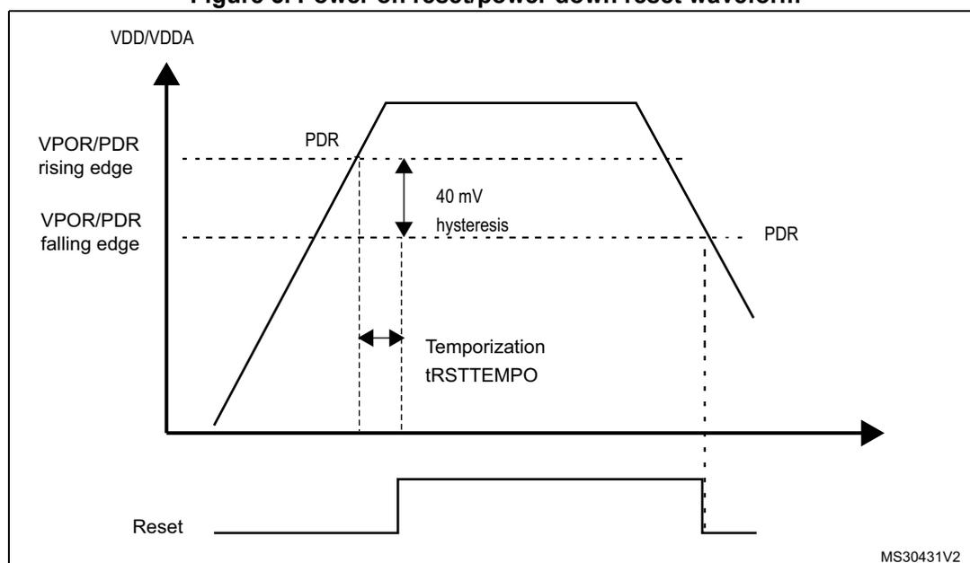
5.2.1 Power on reset (POR)/power down reset (PDR)
The device has an integrated POR/PDR circuitry that allows proper operation starting from/down to 2 V.
The device remains in Reset mode when \( V_{DD}/V_{DDA} \) is below a specified threshold, \( V_{POR/PDR} \) , without the need for an external reset circuit. For more details concerning the power on/power down reset threshold, refer to the electrical characteristics of the datasheet.
Figure 5. Power on reset/power down reset waveform
5.2.2 Programmable voltage detector (PVD)
The PVD can be used to monitor the \( V_{DD}/V_{DDA} \) power supply by comparing it to a threshold selected by the PLS[2:0] bits in the Power control register (PWR_CR) .
The PVD is enabled by setting the PVDE bit.
A PVDO flag is available, in the Power control/status register (PWR_CSR) , to indicate if \( V_{DD}/V_{DDA} \) is higher or lower than the PVD threshold. This event is internally connected to the EXTI line16 and can generate an interrupt if enabled through the EXTI registers. The PVD output interrupt can be generated when \( V_{DD}/V_{DDA} \) drops below the PVD threshold and/or when \( V_{DD}/V_{DDA} \) rises above the PVD threshold depending on EXTI line16 rising/falling edge configuration. As an example the service routine could perform emergency shutdown tasks.
Figure 6. PVD thresholds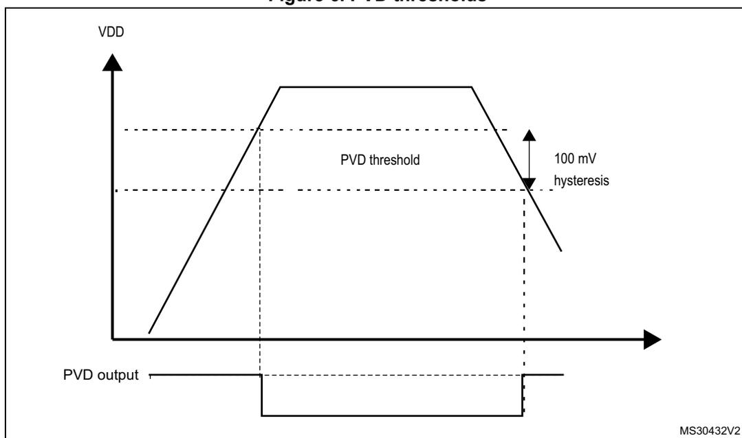
The figure illustrates the relationship between the supply voltage ( \( V_{DD} \) ) and the Power Supply Voltage Detector (PVD) output. The top graph shows \( V_{DD} \) rising to a peak and then falling. A dashed horizontal line represents the PVD threshold. As \( V_{DD} \) falls, the PVD output (bottom graph) changes state. The hysteresis is indicated by a 100 mV difference between the rising and falling thresholds. The code MS30432V2 is visible in the bottom right corner.
5.3 Low-power modes
By default, the microcontroller is in Run mode after a system or a power Reset. Several low-power modes are available to save power when the CPU does not need to be kept running, for example when waiting for an external event. It is up to the user to select the mode that gives the best compromise between low-power consumption, short startup time and available wakeup sources.
The STM32F10xxx devices feature three low-power modes:
- • Sleep mode (CPU clock off, all peripherals including Cortex®-M3 core peripherals like NVIC, SysTick, etc. are kept running)
- • Stop mode (all clocks are stopped)
- • Standby mode (1.8V domain powered-off)
In addition, the power consumption in Run mode can be reduced by one of the following means:
- • Slowing down the system clocks
- • Gating the clocks to the APB and AHB peripherals when they are unused.
Table 11. Low-power mode summary
| Mode name | Entry | Wakeup | Effect on 1.8V domain clocks | Effect on V DD domain clocks | Voltage regulator |
|---|---|---|---|---|---|
| Sleep (Sleep now or Sleep-on -exit) | WFI | Any interrupt | CPU clock OFF no effect on other clocks or analog clock sources | None | ON |
| WFE | Wakeup event | ||||
| Stop | PDDS and LPDS bits + SLEEPDEEP bit + WFI or WFE | Any EXTI line (configured in the EXTI registers) | All 1.8V domain clocks OFF | HSI and HSE oscillators OFF | ON or in low-power mode (depends on Power control register (PWR_CR) ) |
| Standby | PDDS bit + SLEEPDEEP bit + WFI or WFE | WKUP pin rising edge, RTC alarm, external reset in NRST pin, IWDG reset | OFF |
5.3.1 Slowing down system clocks
In Run mode the speed of the system clocks (SYSCLK, HCLK, PCLK1, PCLK2) can be reduced by programming the prescaler registers. These prescalers can also be used to slow down peripherals before entering Sleep mode.
For more details refer to Section 7.3.2: Clock configuration register (RCC_CFGR) .
5.3.2 Peripheral clock gating
In Run mode, the HCLK and PCLKx for individual peripherals and memories can be stopped at any time to reduce power consumption.
To further reduce power consumption in Sleep mode the peripheral clocks can be disabled prior to executing the WFI or WFE instructions.
Peripheral clock gating is controlled by the AHB peripheral clock enable register (RCC_AHBENR) , APB1 peripheral clock enable register (RCC_APB1ENR) and APB2 peripheral clock enable register (RCC_APB2ENR) .
5.3.3 Sleep mode
Entering Sleep mode
The Sleep mode is entered by executing the WFI (Wait For Interrupt) or WFE (Wait for Event) instructions. Two options are available to select the Sleep mode entry mechanism, depending on the SLEEPONEXIT bit in the Cortex®-M3 System Control register:
- • Sleep-now: if the SLEEPONEXIT bit is cleared, the MCU enters Sleep mode as soon as WFI or WFE instruction is executed.
- • Sleep-on-exit: if the SLEEPONEXIT bit is set, the MCU enters Sleep mode as soon as it exits the lowest priority ISR.
In the Sleep mode, all I/O pins keep the same state as in the Run mode.
Refer to Table 12 and Table 13 for details on how to enter Sleep mode.
Exiting Sleep mode
If the WFI instruction is used to enter Sleep mode, any peripheral interrupt acknowledged by the nested vectored interrupt controller (NVIC) can wake up the device from Sleep mode.
If the WFE instruction is used to enter Sleep mode, the MCU exits Sleep mode as soon as an event occurs. The wakeup event can be generated either by:
- • enabling an interrupt in the peripheral control register but not in the NVIC, and enabling the SEVONPEND bit in the Cortex®-M3 System Control register. When the MCU resumes from WFE, the peripheral interrupt pending bit and the peripheral NVIC IRQ channel pending bit (in the NVIC interrupt clear pending register) have to be cleared.
- • or configuring an external or internal EXTI line in event mode. When the CPU resumes from WFE, it is not necessary to clear the peripheral interrupt pending bit or the NVIC IRQ channel pending bit as the pending bit corresponding to the event line is not set.
This mode offers the lowest wakeup time as no time is wasted in interrupt entry/exit.
Refer to Table 12 and Table 13 for more details on how to exit Sleep mode.
Table 12. Sleep-now
| Sleep-now mode | Description |
|---|---|
| Mode entry | WFI (Wait for Interrupt) or WFE (Wait for Event) while: – SLEEPDEEP = 0 and – SLEEPONEXIT = 0 Refer to the Cortex®-M3 System Control register. |
| Mode exit | If WFI was used for entry: Interrupt: Refer to Section 10.1.2: Interrupt and exception vectors If WFE was used for entry Wakeup event: Refer to Section 10.2.3: Wakeup event management |
| Wakeup latency | None |
Table 13. Sleep-on-exit
| Sleep-on-exit | Description |
|---|---|
| Mode entry | WFI (wait for interrupt) while: – SLEEPDEEP = 0 and – SLEEPONEXIT = 1 Refer to the Cortex®-M3 System Control register. |
| Mode exit | Interrupt: refer to Section 10.1.2: Interrupt and exception vectors . |
| Wakeup latency | None |
5.3.4 Stop mode
The Stop mode is based on the Cortex®-M3 deepsleep mode combined with peripheral clock gating. The voltage regulator can be configured either in normal or low-power mode. In Stop mode, all clocks in the 1.8 V domain are stopped, the PLL, the HSI and the HSE RC oscillators are disabled. SRAM and register contents are preserved.
In the Stop mode, all I/O pins keep the same state as in the Run mode.
Entering Stop mode
Refer to Table 14 for details on how to enter the Stop mode.
To further reduce power consumption in Stop mode, the internal voltage regulator can be put in low-power mode. This is configured by the LPDS bit of the Power control register (PWR_CR) .
If Flash memory programming is ongoing, the Stop mode entry is delayed until the memory access is finished.
If an access to the APB domain is ongoing, The Stop mode entry is delayed until the APB access is finished.
In Stop mode, the following features can be selected by programming individual control bits:
- • Independent watchdog (IWDG): the IWDG is started by writing to its Key register or by hardware option. Once started it cannot be stopped except by a Reset. See Section 19.3: IWDG functional description .
- • Real-time clock (RTC): this is configured by the RTCEN bit in the Backup domain control register (RCC_BDCR)
- • Internal RC oscillator (LSI RC): this is configured by the LSION bit in the Control/status register (RCC_CSR) .
- • External 32.768 kHz oscillator (LSE OSC): this is configured by the LSEON bit in the Backup domain control register (RCC_BDCR) .
The ADC or DAC can also consume power during the Stop mode, unless they are disabled before entering it. To disable them, the ADON bit in the ADC_CR2 register and the ENx bit in the DAC_CR register must both be written to 0.
Note: If the application needs to disable the external clock before entering Stop mode, the HSEON bit must first be disabled and the system clock switched to HSI. Otherwise, if the HSEON bit remains enabled and the external clock (external oscillator) is removed when entering Stop mode, the clock security system (CSS) feature must be enabled to detect any external oscillator failure and avoid a malfunction behavior when entering stop mode.
Exiting Stop mode
Refer to Table 14 for more details on how to exit Stop mode.
When exiting Stop mode by issuing an interrupt or a wakeup event, the HSI RC oscillator is selected as system clock.
When the voltage regulator operates in low-power mode, an additional startup delay is incurred when waking up from Stop mode. By keeping the internal regulator ON during Stop mode, the consumption is higher although the startup time is reduced.
Table 14. Stop mode
| Stop mode | Description |
|---|---|
| Mode entry | WFI (Wait for Interrupt) or WFE (Wait for Event) while:
Note: To enter Stop mode, all EXTI Line pending bits (in Pending register (EXTI_PR) ), all peripheral interrupt pending bits, and RTC Alarm flag must be reset. Otherwise, the Stop mode entry procedure is ignored and program execution continues. |
| Mode exit | If WFI was used for entry: Any EXTI Line configured in Interrupt mode (the corresponding EXTI Interrupt vector must be enabled in the NVIC). Refer to Section 10.1.2: Interrupt and exception vectors . If WFE was used for entry: Any EXTI Line configured in event mode. Refer to Section 10.2.3: Wakeup event management |
| Wakeup latency | HSI RC wakeup time + regulator wakeup time from Low-power mode |
5.3.5 Standby mode
The Standby mode allows to achieve the lowest power consumption. It is based on the Cortex®-M3 deepsleep mode, with the voltage regulator disabled. The 1.8 V domain is consequently powered off. The PLL, the HSI oscillator and the HSE oscillator are also switched off. SRAM and register contents are lost except for registers in the Backup domain and Standby circuitry (see Figure 4 ).
Entering Standby mode
Refer to Table 15 for more details on how to enter Standby mode.
In Standby mode, the following features can be selected by programming individual control bits:
- • Independent watchdog (IWDG): the IWDG is started by writing to its Key register or by hardware option. Once started it cannot be stopped except by a reset. See Section 19.3: IWDG functional description .
- • Real-time clock (RTC): this is configured by the RTCEN bit in the Backup domain control register (RCC_BDCR)
- • Internal RC oscillator (LSI RC): this is configured by the LSION bit in the Control/status register (RCC_CSR).
- • External 32.768 kHz oscillator (LSE OSC): this is configured by the LSEON bit in the Backup domain control register (RCC_BDCR)
Exiting Standby mode
The microcontroller exits the Standby mode when an external reset (NRST pin), an IWDG reset, a rising edge on the WKUP pin or the rising edge of an RTC alarm occurs (see Figure 179: RTC simplified block diagram ). All registers are reset after wakeup from Standby except for Power control/status register (PWR_CSR) .
After waking up from Standby mode, program execution restarts in the same way as after a Reset (boot pins sampling, vector reset is fetched, etc.). The SBF status flag in the Power control/status register (PWR_CSR) indicates that the MCU was in Standby mode.
Refer to Table 15 for more details on how to exit Standby mode.
Table 15. Standby mode
| Standby mode | Description |
|---|---|
| Mode entry | WFI (Wait for Interrupt) or WFE (Wait for Event) while:
|
| Mode exit | WKUP pin rising edge, RTC alarm event's rising edge, external Reset in NRST pin, IWDG Reset. |
| Wakeup latency | Reset phase |
I/O states in Standby mode
In Standby mode, all I/O pins are high impedance except:
- • Reset pad (still available)
- • TAMPER pin if configured for tamper or calibration out
- • WKUP pin, if enabled
Debug mode
By default, the debug connection is lost if the application puts the MCU in Stop or Standby mode while the debug features are used. This is due to the fact that the Cortex®-M3 core is no longer clocked.
However, by setting some configuration bits in the DBGMCU_CR register, the software can be debugged even when using the low-power modes extensively. For more details, refer to Section 31.16.1: Debug support for low-power modes .
5.3.6 Auto-wakeup (AWU) from low-power mode
The RTC can be used to wakeup the MCU from low-power mode without depending on an external interrupt (Auto-wakeup mode). The RTC provides a programmable time base for waking up from Stop or Standby mode at regular intervals. For this purpose, two of the three alternative RTC clock sources can be selected by programming the RTCSEL[1:0] bits in the Backup domain control register (RCC_BDCR) :
- • Low-power 32.768 kHz external crystal oscillator (LSE OSC).
This clock source provides a precise time base with very low-power consumption (less than 1µA added consumption in typical conditions) - • Low-power internal RC Oscillator (LSI RC)
This clock source has the advantage of saving the cost of the 32.768 kHz crystal. This internal RC Oscillator is designed to add minimum power consumption.
To wakeup from Stop mode with an RTC alarm event, it is necessary to:
- • Configure the EXTI Line 17 to be sensitive to rising edge
- • Configure the RTC to generate the RTC alarm
To wakeup from Standby mode, there is no need to configure the EXTI Line 17.
5.4 Power control registers
The peripheral registers can be accessed by half-words (16-bit) or words (32-bit).
5.4.1 Power control register (PWR_CR)
Address offset: 0x00
Reset value: 0x0000 0000 (reset by wakeup from Standby mode)
| 31 | 30 | 29 | 28 | 27 | 26 | 25 | 24 | 23 | 22 | 21 | 20 | 19 | 18 | 17 | 16 |
|---|---|---|---|---|---|---|---|---|---|---|---|---|---|---|---|
| Reserved | |||||||||||||||
| 15 | 14 | 13 | 12 | 11 | 10 | 9 | 8 | 7 | 6 | 5 | 4 | 3 | 2 | 1 | 0 |
| Reserved | DBP | PLS[2:0] | PVDE | CSBF | CWUF | PDDS | LPDS | ||||||||
| rw | rw | rw | rw | rw | rc_w1 | rc_w1 | rw | rw | |||||||
Bits 31:9 Reserved, must be kept at reset value..
Bit 8 DBP : Disable backup domain write protection.
In reset state, the RTC and backup registers are protected against parasitic write access.
This bit must be set to enable write access to these registers.
0: Access to RTC and Backup registers disabled
1: Access to RTC and Backup registers enabled
Note: If the HSE divided by 128 is used as the RTC clock, this bit must remain set to 1.
Bits 7:5 PLS[2:0] : PVD level selection.
These bits are written by software to select the voltage threshold detected by the programmable voltage detector
000: 2.2V
001: 2.3V
010: 2.4V
011: 2.5V
100: 2.6V
101: 2.7V
110: 2.8V
111: 2.9V
Note: Refer to the electrical characteristics of the datasheet for more details.
Bit 4 PVDE : programmable voltage detector enable.
This bit is set and cleared by software.
0: PVD disabled
1: PVD enabled
Bit 3 CSBF : Clear standby flag.
This bit is always read as 0.
0: No effect
1: Clear the SBF Standby Flag (write).
Bit 2 CWUF : Clear wakeup flag.
This bit is always read as 0.
0: No effect
1: Clear the WUF Wakeup Flag after 2 System clock cycles . (write)
Bit 1 PDDS : Power down deepsleep.
This bit is set and cleared by software. It works together with the LPDS bit.
0: Enter Stop mode when the CPU enters Deep sleep. The regulator status depends on the LPDS bit.
1: Enter Standby mode when the CPU enters Deep sleep.
Bit 0 LPDS : Low-power deepsleep.
This bit is set and cleared by software. It works together with the PDDS bit.
0: Voltage regulator on during Stop mode
1: Voltage regulator in low-power mode during Stop mode
5.4.2 Power control/status register (PWR_CSR)
Address offset: 0x04
Reset value: 0x0000 0000 (not reset by wakeup from Standby mode)
Additional APB cycles are needed to read this register versus a standard APB read.
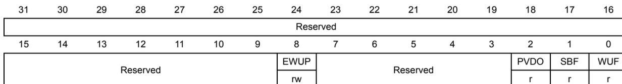
| 31 | 30 | 29 | 28 | 27 | 26 | 25 | 24 | 23 | 22 | 21 | 20 | 19 | 18 | 17 | 16 |
| Reserved | |||||||||||||||
| 15 | 14 | 13 | 12 | 11 | 10 | 9 | 8 | 7 | 6 | 5 | 4 | 3 | 2 | 1 | 0 |
| Reserved | EWUP | Reserved | PVDO | SBF | WUF | ||||||||||
| rw | r | r | r | ||||||||||||
Bits 31:9 Reserved, must be kept at reset value.
Bit 8 EWUP : Enable WKUP pin
This bit is set and cleared by software.
- 0: WKUP pin is used for general purpose I/O. An event on the WKUP pin does not wakeup the device from Standby mode.
- 1: WKUP pin is used for wakeup from Standby mode and forced in input pull down configuration (rising edge on WKUP pin wakes-up the system from Standby mode).
Note: This bit is reset by a system Reset.
Bits 7:3 Reserved, must be kept at reset value.
Bit 2 PVDO : PVD output
This bit is set and cleared by hardware. It is valid only if PVD is enabled by the PVDE bit.
- 0: \( V_{DD}/V_{DDA} \) is higher than the PVD threshold selected with the PLS[2:0] bits.
- 1: \( V_{DD}/V_{DDA} \) is lower than the PVD threshold selected with the PLS[2:0] bits.
Note: The PVD is stopped by Standby mode. For this reason, this bit is equal to 0 after Standby or reset until the PVDE bit is set.
Bit 1 SBF : Standby flag
This bit is set by hardware and cleared only by a POR/PDR (power on reset/power down reset) or by setting the CSBF bit in the Power control register (PWR_CR)
- 0: Device has not been in Standby mode
- 1: Device has been in Standby mode
Bit 0 WUF : Wakeup flag
This bit is set by hardware and cleared by hardware, by a system reset or by setting the CWUF bit in the Power control register (PWR_CR)
- 0: No wakeup event occurred
- 1: A wakeup event was received from the WKUP pin or from the RTC alarm
Note: An additional wakeup event is detected if the WKUP pin is enabled (by setting the EWUP bit) when the WKUP pin level is already high.
5.4.3 PWR register map
The following table summarizes the PWR registers.
Table 16. PWR register map and reset values
| Offset | Register | 31 | 30 | 29 | 28 | 27 | 26 | 25 | 24 | 23 | 22 | 21 | 20 | 19 | 18 | 17 | 16 | 15 | 14 | 13 | 12 | 11 | 10 | 9 | 8 | 7 | 6 | 5 | 4 | 3 | 2 | 1 | 0 |
|---|---|---|---|---|---|---|---|---|---|---|---|---|---|---|---|---|---|---|---|---|---|---|---|---|---|---|---|---|---|---|---|---|---|
| 0x000 | PWR_CR | Reserved | DBP | PLS [2:0] | PVDE | CSBF | CWUF | PDDS | LPDS | ||||||||||||||||||||||||
| Reset value | 0 | 0 | 0 | 0 | 0 | 0 | 0 | 0 | 0 | 0 | |||||||||||||||||||||||
| 0x004 | PWR_CSR | Reserved | EWUP | Reserved | PVDO | SBF | WUF | ||||||||||||||||||||||||||
| Reset value | 0 | 0 | 0 | 0 | 0 | 0 | 0 | ||||||||||||||||||||||||||
Refer to Table 3 on page 50 for the register boundary addresses.