2. Documentation conventions
2.1 General information
The STM32F10xxx devices have an Arm ®(a) Cortex ® -M3 core.
2.2 List of abbreviations for registers
The following abbreviations are used in register descriptions:
| read/write (rw) | Software can read and write to these bits. |
| read-only (r) | Software can only read these bits. |
| write-only (w) | Software can only write to this bit. Reading the bit returns the reset value. |
| read/clear (rc_w1) | Software can read as well as clear this bit by writing 1. Writing '0' has no effect on the bit value. |
| read/clear (rc_w0) | Software can read as well as clear this bit by writing 0. Writing '1' has no effect on the bit value. |
| read/clear by read (rc_r) | Software can read this bit. Reading this bit automatically clears it to '0'. Writing '0' has no effect on the bit value. |
| read/set (rs) | Software can read as well as set this bit. Writing '0' has no effect on the bit value. |
| read-only write trigger (rt_w) | Software can read this bit. Writing '0' or '1' triggers an event but has no effect on the bit value. |
| toggle (t) | Software can only toggle this bit by writing '1'. Writing '0' has no effect. |
| Reserved (Res.) | Reserved bit, must be kept at reset value. |

a. Arm is a registered trademark of Arm Limited (or its subsidiaries) in the US and/or elsewhere.
2.3 Glossary
- • Low-density devices are STM32F101xx, STM32F102xx and STM32F103xx microcontrollers where the Flash memory density ranges between 16 and 32 Kbytes.
- • Medium-density devices are STM32F101xx, STM32F102xx and STM32F103xx microcontrollers where the Flash memory density ranges between 64 and 128 Kbytes.
- • High-density devices are STM32F101xx and STM32F103xx microcontrollers where the Flash memory density ranges between 256 and 512 Kbytes.
- • XL-density devices are STM32F101xx and STM32F103xx microcontrollers where the Flash memory density ranges between 768 Kbytes and 1 Mbyte.
- • Connectivity line devices are STM32F105xx and STM32F107xx microcontrollers.
- • Word : data of 32-bit length.
- • Half-word : data of 16-bit length.
- • Byte : data of 8-bit length.
2.4 Peripheral availability
For peripheral availability and number across all STM32F10xxx sales types, refer to the low-, medium-, high- and XL-density STM32F101xx and STM32F103xx datasheets, to the low- and medium-density STM32F102xx datasheets and to the connectivity line devices, STM32F105xx/STM32F107xx.
3 Memory and bus architecture
3.1 System architecture
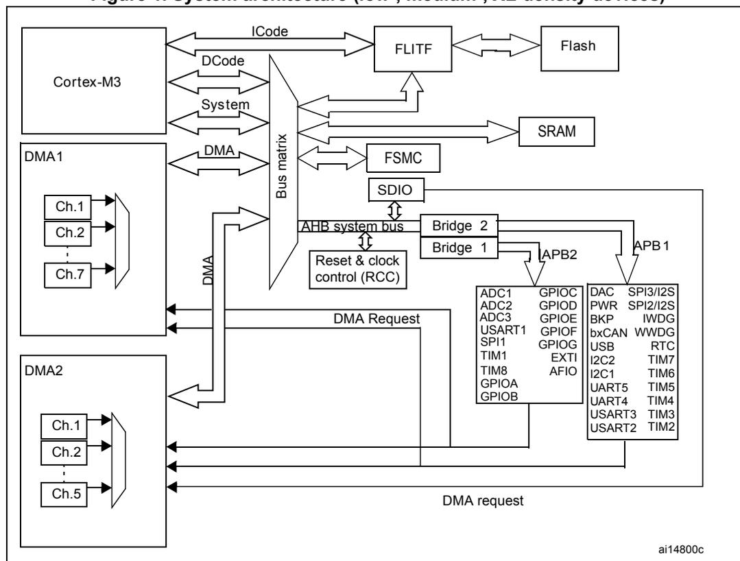
In low-, medium-, high- and XL-density devices, the main system consists of:
- • Four masters:
- – Cortex ® -M3 core DCode bus (D-bus) and System bus (S-bus)
- – GP-DMA1 & 2 (general-purpose DMA)
- • Four slaves:
- – Internal SRAM
- – Internal Flash memory
- – FSMC
- – AHB to APBx (APB1 or APB2), which connect all the APB peripherals
These are interconnected using a multilayer AHB bus architecture as shown in Figure 1 :
Figure 1. System architecture (low-, medium-, XL-density devices)
In connectivity line devices the main system consists of:
- • Five masters:
- – Cortex ® -M3 core DCode bus (D-bus) and System bus (S-bus)
- – GP-DMA1 & 2 (general-purpose DMA)
- – Ethernet DMA
- • Three slaves:
- – Internal SRAM
- – Internal Flash memory
- – AHB to APB bridges (AHB to APBx), which connect all the APB peripherals
These are interconnected using a multilayer AHB bus architecture as shown in Figure 2 :
Figure 2. System architecture in connectivity line devices
ICode bus
This bus connects the Instruction bus of the Cortex ® -M3 core to the Flash memory instruction interface. Prefetching is performed on this bus.
DCode bus
This bus connects the DCode bus (literal load and debug access) of the Cortex ® -M3 core to the Flash memory Data interface.
System bus
This bus connects the system bus of the Cortex ® -M3 core (peripherals bus) to a BusMatrix which manages the arbitration between the core and the DMA.
DMA bus
This bus connects the AHB master interface of the DMA to the BusMatrix which manages the access of CPU DCode and DMA to SRAM, Flash memory and peripherals.
BusMatrix
The BusMatrix manages the access arbitration between the core system bus and the DMA master bus. The arbitration uses a Round Robin algorithm. In connectivity line devices, the BusMatrix is composed of five masters (CPU DCode, System bus, Ethernet DMA, DMA1 and DMA2 bus) and three slaves (FLITF, SRAM and AHB2APB bridges). In other devices, the BusMatrix is composed of four masters (CPU DCode, System bus, DMA1 bus and DMA2 bus) and four slaves (FLITF, SRAM, FSMC and AHB2APB bridges).
AHB peripherals are connected on system bus through a BusMatrix to allow DMA access.
AHB/APB bridges (APB)
The two AHB/APB bridges provide full synchronous connections between the AHB and the 2 APB buses. APB1 is limited to 36 MHz, APB2 operates at full speed (up to 72 MHz depending on the device).
Refer to Table 3 for the address mapping of the peripherals connected to each bridge.
After each device reset, all peripheral clocks are disabled (except for the SRAM and FLITF). Before using a peripheral you have to enable its clock in the RCC_AHBENR, RCC_APB2ENR or RCC_APB1ENR register.
Note: When a 16- or 8-bit access is performed on an APB register, the access is transformed into a 32-bit access: the bridge duplicates the 16- or 8-bit data to feed the 32-bit vector.
3.2 Memory organization
Program memory, data memory, registers and I/O ports are organized within the same linear 4-Gbyte address space.
The bytes are coded in memory in Little Endian format. The lowest numbered byte in a word is considered the word's least significant byte and the highest numbered byte the most significant.
For the detailed mapping of peripheral registers refer to the related sections.
The addressable memory space is divided into 8 main blocks, each of 512 MB.
All the memory areas that are not allocated to on-chip memories and peripherals are considered "Reserved"). Refer to the Memory map figure in the corresponding product datasheet.
3.3 Memory map
See the datasheet corresponding to your device for a comprehensive diagram of the memory map. Table 3 gives the boundary addresses of the peripherals available in all STM32F10xxx devices.
Table 3. Register boundary addresses
| Boundary address | Peripheral | Bus | Register map |
|---|---|---|---|
| 0xA000 0000 - 0xA000 0FFF | FSMC | AHB | Section 21.6.9 on page 564 |
| 0x5000 0000 - 0x5003 FFFF | USB OTG FS | Section 28.16.6 on page 913 | |
| 0x4003 0000 - 0x4FFF FFFF | Reserved | - | |
| 0x4002 8000 - 0x4002 9FFF | Ethernet | Section 29.8.5 on page 1071 | |
| 0x4002 3400 - 0x4002 7FFF | Reserved | - | |
| 0x4002 3000 - 0x4002 33FF | CRC | Section 4.4.4 on page 65 | |
| 0x4002 2000 - 0x4002 23FF | Flash memory interface | - | |
| 0x4002 1400 - 0x4002 1FFF | Reserved | - | |
| 0x4002 1000 - 0x4002 13FF | Reset and clock control RCC | Section 7.3.11 on page 121 | |
| 0x4002 0800 - 0x4002 0FFF | Reserved | - | |
| 0x4002 0400 - 0x4002 07FF | DMA2 | Section 13.4.7 on page 289 | |
| 0x4002 0000 - 0x4002 03FF | DMA1 | ||
| 0x4001 8400 - 0x4001 FFFF | Reserved | - | |
| 0x4001 8000 - 0x4001 83FF | SDIO | Section 22.9.16 on page 621 |
Table 3. Register boundary addresses (continued)
| Boundary address | Peripheral | Bus | Register map |
|---|---|---|---|
| 0x4001 5800 - 0x4001 7FFF | Reserved | APB2 | - |
| 0x4001 5400 - 0x4001 57FF | TIM11 timer | Section 16.5.11 on page 468 | |
| 0x4001 5000 - 0x4001 53FF | TIM10 timer | Section 16.5.11 on page 468 | |
| 0x4001 4C00 - 0x4001 4FFF | TIM9 timer | Section 16.4.13 on page 458 | |
| 0x4001 4000 - 0x4001 4BFF | Reserved | - | |
| 0x4001 3C00 - 0x4001 3FFF | ADC3 | Section 11.12.15 on page 252 | |
| 0x4001 3800 - 0x4001 3BFF | USART1 | Section 27.6.8 on page 827 | |
| 0x4001 3400 - 0x4001 37FF | TIM8 timer | Section 14.4.21 on page 363 | |
| 0x4001 3000 - 0x4001 33FF | SPI1 | Section 25.5 on page 742 | |
| 0x4001 2C00 - 0x4001 2FFF | TIM1 timer | Section 14.4.21 on page 363 | |
| 0x4001 2800 - 0x4001 2BFF | ADC2 | Section 11.12.15 on page 252 | |
| 0x4001 2400 - 0x4001 27FF | ADC1 | ||
| 0x4001 2000 - 0x4001 23FF | GPIO Port G | Section 9.5 on page 194 | |
| 0x4001 1C00 - 0x4001 1FFF | GPIO Port F | ||
| 0x4001 1800 - 0x4001 1BFF | GPIO Port E | ||
| 0x4001 1400 - 0x4001 17FF | GPIO Port D | ||
| 0x4001 1000 - 0x4001 13FF | GPIO Port C | ||
| 0x4001 0C00 - 0x4001 0FFF | GPIO Port B | ||
| 0x4001 0800 - 0x4001 0BFF | GPIO Port A | ||
| 0x4001 0400 - 0x4001 07FF | EXTI | Section 10.3.7 on page 214 | |
| 0x4001 0000 - 0x4001 03FF | AFIO | Section 9.5 on page 194 |
Table 3. Register boundary addresses (continued)
| Boundary address | Peripheral | Bus | Register map |
|---|---|---|---|
| 0x4000 7800 - 0x4000 FFFF | Reserved | - | |
| 0x4000 7400 - 0x4000 77FF | DAC | Section 12.5.14 on page 273 | |
| 0x4000 7000 - 0x4000 73FF | Power control PWR | Section 5.4.3 on page 80 | |
| 0x4000 6C00 - 0x4000 6FFF | Backup registers (BKP) | Section 6.4.5 on page 85 | |
| 0x4000 6400 - 0x4000 67FF | bxCAN1 | Section 24.9.5 on page 695 | |
| 0x4000 6800 - 0x4000 6BFF | bxCAN2 | ||
| 0x4000 6000 (1) - 0x4000 63FF | Shared USB/CAN SRAM 512 bytes | - | |
| 0x4000 5C00 - 0x4000 5FFF | USB device FS registers | Section 23.5.4 on page 651 | |
| 0x4000 5800 - 0x4000 5BFF | I2C2 | Section 26.6.10 on page 784 | |
| 0x4000 5400 - 0x4000 57FF | I2C1 | ||
| 0x4000 5000 - 0x4000 53FF | UART5 | Section 27.6.8 on page 827 | |
| 0x4000 4C00 - 0x4000 4FFF | UART4 | ||
| 0x4000 4800 - 0x4000 4BFF | USART3 | ||
| 0x4000 4400 - 0x4000 47FF | USART2 | ||
| 0x4000 4000 - 0x4000 43FF | Reserved | - | |
| 0x4000 3C00 - 0x4000 3FFF | SPI3/I2S | APB1 | Section 25.5 on page 742 |
| 0x4000 3800 - 0x4000 3BFF | SPI2/I2S | Section 25.5 on page 742 | |
| 0x4000 3400 - 0x4000 37FF | Reserved | - | |
| 0x4000 3000 - 0x4000 33FF | Independent watchdog (IWDG) | Section 19.4.5 on page 499 | |
| 0x4000 2C00 - 0x4000 2FFF | Window watchdog (WWDG) | Section 20.6.4 on page 506 | |
| 0x4000 2800 - 0x4000 2BFF | RTC | Section 18.4.7 on page 493 | |
| 0x4000 2400 - 0x4000 27FF | Reserved | - | |
| 0x4000 2000 - 0x4000 23FF | TIM14 timer | Section 16.5.11 on page 468 | |
| 0x4000 1C00 - 0x4000 1FFF | TIM13 timer | ||
| 0x4000 1800 - 0x4000 1BFF | TIM12 timer | Section 16.4.13 on page 458 | |
| 0x4000 1400 - 0x4000 17FF | TIM7 timer | Section 17.4.9 on page 481 | |
| 0x4000 1000 - 0x4000 13FF | TIM6 timer | ||
| 0x4000 0C00 - 0x4000 0FFF | TIM5 timer | Section 15.4.19 on page 423 | |
| 0x4000 0800 - 0x4000 0BFF | TIM4 timer | ||
| 0x4000 0400 - 0x4000 07FF | TIM3 timer | ||
| 0x4000 0000 - 0x4000 03FF | TIM2 timer |
1. This shared SRAM can be fully accessed only in low-, medium-, high- and XL-density devices, not in connectivity line devices.
3.3.1 Embedded SRAM
The STM32F10xxx features up to 96 Kbytes of static SRAM. It can be accessed as bytes, half-words (16 bits) or full words (32 bits). The SRAM start address is 0x2000 0000.
3.3.2 Bit banding
The Cortex ® -M3 memory map includes two bit-band regions. These regions map each word in an alias region of memory to a bit in a bit-band region of memory. Writing to a word in the alias region has the same effect as a read-modify-write operation on the targeted bit in the bit-band region.
In the STM32F10xxx both peripheral registers and SRAM are mapped in a bit-band region. This allows single bit-band write and read operations to be performed. The operations are only available for Cortex ® -M3 accesses, not from other bus masters (e.g. DMA).
A mapping formula shows how to reference each word in the alias region to a corresponding bit in the bit-band region. The mapping formula is:
where:
bit_word_addr is the address of the word in the alias memory region that maps to the targeted bit.
bit_band_base is the starting address of the alias region
byte_offset is the number of the byte in the bit-band region that contains the targeted bit
bit_number is the bit position (0-7) of the targeted bit.
Example:
The following example shows how to map bit 2 of the byte located at SRAM address 0x20000300 in the alias region:
Writing to address 0x22006008 has the same effect as a read-modify-write operation on bit 2 of the byte at SRAM address 0x20000300.
Reading address 0x22006008 returns the value (0x01 or 0x00) of bit 2 of the byte at SRAM address 0x20000300 (0x01: bit set; 0x00: bit reset).
For more information on Bit-Banding refer to the Cortex ® -M3 Technical Reference Manual .
3.3.3 Embedded Flash memory
The high-performance Flash memory module has the following key features:
- • For XL-density devices: density of up to 1 Mbyte with dual bank architecture for read-while-write (RWW) capability:
- – bank 1: fixed size of 512 Kbytes
- – bank 2: up to 512 Kbytes
- • For other devices: density of up to 512 Kbytes
- • Memory organization: the Flash memory is organized as a main block and an information block:
- – Main memory block of size:
- up to 128 Kbytes × 64 bits divided into 512 pages of 2 Kbytes each (see Table 8 ) for XL-density devices
- up to 4 Kb × 64 bits divided into 32 pages of 1 Kbyte each for low-density devices (see Table 4 )
- up to 16 Kb × 64 bits divided into 128 pages of 1 Kbyte each for medium-density devices (see Table 5 )
- up to 64 Kb × 64 bits divided into 256 pages of 2 Kbytes each (see Table 6 ) for high-density devices
- up to 32 Kbit × 64 bits divided into 128 pages of 2 Kbytes each (see Table 7 ) for connectivity line devices
- – Information block of size:
- – Main memory block of size:
The Flash memory interface (FLITF) features:
- • Read interface with prefetch buffer (2x64-bit words)
- • Option byte Loader
- • Flash Program / Erase operation
- • Read / Write protection
Table 4. Flash module organization (low-density devices)
| Block | Name | Base addresses | Size (bytes) |
|---|---|---|---|
| Main memory | Page 0 | 0x0800 0000 - 0x0800 03FF | 1 K |
| Page 1 | 0x0800 0400 - 0x0800 07FF | 1 K | |
| Page 2 | 0x0800 0800 - 0x0800 0BFF | 1 K | |
| Page 3 | 0x0800 0C00 - 0x0800 0FFF | 1 K | |
| Page 4 | 0x0800 1000 - 0x0800 13FF | 1 K | |
| ⋮ | ⋮ | ⋮ | |
| Page 31 | 0x0800 7C00 - 0x0800 7FFF | 1 K |
| Block | Name | Base addresses | Size (bytes) |
|---|---|---|---|
| Information block | System memory | 0x1FFF F000 - 0x1FFF F7FF | 2 K |
| Option bytes | 0x1FFF F800 - 0x1FFF F80F | 16 | |
| Flash memory interface registers | FLASH_ACR | 0x4002 2000 - 0x4002 2003 | 4 |
| FLASH_KEYR | 0x4002 2004 - 0x4002 2007 | 4 | |
| FLASH_OPTKEYR | 0x4002 2008 - 0x4002 200B | 4 | |
| FLASH_SR | 0x4002 200C - 0x4002 200F | 4 | |
| FLASH_CR | 0x4002 2010 - 0x4002 2013 | 4 | |
| FLASH_AR | 0x4002 2014 - 0x4002 2017 | 4 | |
| Reserved | 0x4002 2018 - 0x4002 201B | 4 | |
| FLASH_OBR | 0x4002 201C - 0x4002 201F | 4 | |
| FLASH_WRPR | 0x4002 2020 - 0x4002 2023 | 4 |
| Block | Name | Base addresses | Size (bytes) |
|---|---|---|---|
| Main memory | Page 0 | 0x0800 0000 - 0x0800 03FF | 1 K |
| Page 1 | 0x0800 0400 - 0x0800 07FF | 1 K | |
| Page 2 | 0x0800 0800 - 0x0800 0BFF | 1 K | |
| Page 3 | 0x0800 0C00 - 0x0800 0FFF | 1 K | |
| Page 4 | 0x0800 1000 - 0x0800 13FF | 1 K | |
| . | . | . | |
| . | . | . | |
| Page 127 | 0x0801 FC00 - 0x0801 FFFF | 1 K | |
| Information block | System memory | 0x1FFF F000 - 0x1FFF F7FF | 2 K |
| Option bytes | 0x1FFF F800 - 0x1FFF F80F | 16 | |
| Flash memory interface registers | FLASH_ACR | 0x4002 2000 - 0x4002 2003 | 4 |
| FLASH_KEYR | 0x4002 2004 - 0x4002 2007 | 4 | |
| FLASH_OPTKEYR | 0x4002 2008 - 0x4002 200B | 4 | |
| FLASH_SR | 0x4002 200C - 0x4002 200F | 4 | |
| FLASH_CR | 0x4002 2010 - 0x4002 2013 | 4 | |
| FLASH_AR | 0x4002 2014 - 0x4002 2017 | 4 | |
| Reserved | 0x4002 2018 - 0x4002 201B | 4 | |
| FLASH_OBR | 0x4002 201C - 0x4002 201F | 4 | |
| FLASH_WRPR | 0x4002 2020 - 0x4002 2023 | 4 |
Table 6. Flash module organization (high-density devices)
| Block | Name | Base addresses | Size (bytes) |
|---|---|---|---|
| Main memory | Page 0 | 0x0800 0000 - 0x0800 07FF | 2 K |
| Page 1 | 0x0800 0800 - 0x0800 0FFF | 2 K | |
| Page 2 | 0x0800 1000 - 0x0800 17FF | 2 K | |
| Page 3 | 0x0800 1800 - 0x0800 1FFF | 2 K | |
| . | . | . | |
| Page 255 | 0x0807 F800 - 0x0807 FFFF | 2 K | |
| Information block | System memory | 0x1FFF F000 - 0x1FFF F7FF | 2 K |
| Option bytes | 0x1FFF F800 - 0x1FFF F80F | 16 | |
| Flash memory interface registers | FLASH_ACR | 0x4002 2000 - 0x4002 2003 | 4 |
| FLASH_KEYR | 0x4002 2004 - 0x4002 2007 | 4 | |
| FLASH_OPTKEYR | 0x4002 2008 - 0x4002 200B | 4 | |
| FLASH_SR | 0x4002 200C - 0x4002 200F | 4 | |
| FLASH_CR | 0x4002 2010 - 0x4002 2013 | 4 | |
| FLASH_AR | 0x4002 2014 - 0x4002 2017 | 4 | |
| Reserved | 0x4002 2018 - 0x4002 201B | 4 | |
| FLASH_OBR | 0x4002 201C - 0x4002 201F | 4 | |
| FLASH_WRPR | 0x4002 2020 - 0x4002 2023 | 4 |
Table 7. Flash module organization (connectivity line devices)
| Block | Name | Base addresses | Size (bytes) |
|---|---|---|---|
| Main memory | Page 0 | 0x0800 0000 - 0x0800 07FF | 2 K |
| Page 1 | 0x0800 0800 - 0x0800 0FFF | 2 K | |
| Page 2 | 0x0800 1000 - 0x0800 17FF | 2 K | |
| Page 3 | 0x0800 1800 - 0x0800 1FFF | 2 K | |
| . | . | . | |
| Page 127 | 0x0803 F800 - 0x0803 FFFF | 2 K | |
| Information block | System memory | 0x1FFF B000 - 0x1FFF F7FF | 18 K |
| Option bytes | 0x1FFF F800 - 0x1FFF F80F | 16 |
Table 7. Flash module organization (connectivity line devices) (continued)
| Block | Name | Base addresses | Size (bytes) |
|---|---|---|---|
| Flash memory interface registers | FLASH_ACR | 0x4002 2000 - 0x4002 2003 | 4 |
| FLASH_KEYR | 0x4002 2004 - 0x4002 2007 | 4 | |
| FLASH_OPTKEYR | 0x4002 2008 - 0x4002 200B | 4 | |
| FLASH_SR | 0x4002 200C - 0x4002 200F | 4 | |
| FLASH_CR | 0x4002 2010 - 0x4002 2013 | 4 | |
| FLASH_AR | 0x4002 2014 - 0x4002 2017 | 4 | |
| Reserved | 0x4002 2018 - 0x4002 201B | 4 | |
| FLASH_OBR | 0x4002 201C - 0x4002 201F | 4 | |
| FLASH_WRPR | 0x4002 2020 - 0x4002 2023 | 4 |
Table 8. XL-density Flash module organization
| Block | Name | Base addresses | Size (bytes) | |
|---|---|---|---|---|
| Main memory | Bank 1 | Page 0 | 0x0800 0000 - 0x0800 07FF | 2 K |
| Page 1 | 0x0800 0800 - 0x0800 0FFF | 2 K | ||
| ... | ... | ... | ||
| Page 255 | 0x0807 F800 - 0x0807 FFFF | 2 K | ||
| Bank 2 | Page 256 | 0x0808 0000 - 0x0808 07FF | 2 K | |
| Page 257 | 0x0808 0800 - 0x0808 0FFF | 2 K | ||
| . | . | . | ||
| . | . | . | ||
| . | . | . | ||
| Page 511 | 0x080F F800 - 0x080F FFFF | 2 K | ||
| Information block | System memory | 0x1FFF E000 - 0x1FFF F7FF | 6 K | |
| Option bytes | 0x1FFF F800 - 0x1FFF F80F | 16 |
Table 8. XL-density Flash module organization (continued)
| Block | Name | Base addresses | Size (bytes) |
|---|---|---|---|
| Flash memory interface registers | FLASH_ACR | 0x4002 2000 - 0x4002 2003 | 4 |
| FLASH_KEYR | 0x4002 2004 - 0x4002 2007 | 4 | |
| FLASH_OPTKEYR | 0x4002 2008 - 0x4002 200B | 4 | |
| FLASH_SR | 0x4002 200C - 0x4002 200F | 4 | |
| FLASH_CR | 0x4002 2010 - 0x4002 2013 | 4 | |
| FLASH_AR | 0x4002 2014 - 0x4002 2017 | 4 | |
| Reserved | 0x4002 2018 - 0x4002 201B | 4 | |
| FLASH_OBR | 0x4002 201C - 0x4002 201F | 4 | |
| FLASH_WRPR | 0x4002 2020 - 0x4002 2023 | 4 | |
| Reserved | 0x4002 2024 - 0x4002 2043 | 32 | |
| FLASH_KEYR2 | 0x4002 2044 - 0x4002 2047 | 4 | |
| Reserved | 0x4002 2048 - 0x4002 204B | 4 | |
| FLASH_SR2 | 0x4002 204C - 0x4002 204F | 4 | |
| FLASH_CR2 | 0x4002 2050 - 0x4002 2053 | 4 | |
| FLASH_AR2 | 0x4002 2054 - 0x4002 2057 | 4 |
Note: For further information on the Flash memory interface registers, refer to the: “STM32F10xxx XL-density Flash programming manual” (PM0068) for XL-density devices, “STM32F10xxx Flash programming manual” (PM0075) for other devices.
Reading the Flash memory
Flash memory instructions and data access are performed through the AHB bus. The prefetch block is used for instruction fetches through the ICode bus. Arbitration is performed in the Flash memory interface, and priority is given to data access on the DCode bus.
Read accesses can be performed with the following configuration options:
- • Latency: number of wait states for a read operation programmed on-the-fly
- • Prefetch buffer (2 x 64-bit blocks): it is enabled after reset; a whole block can be replaced with a single read from the Flash memory as the size of the block matches the bandwidth of the Flash memory. Thanks to the prefetch buffer, faster CPU execution is possible as the CPU fetches one word at a time with the next word readily available in the prefetch buffer
- • Half cycle: for power optimization
Note: These options have to be used in accordance with the Flash memory access time. The wait states represent the ratio of the SYSCLK (system clock) period to the Flash memory access time:
- - 0 wait states, if \( 0 < \text{SYSCLK} \leq 24 \text{ MHz} \)
- - 1 wait state, if \( 24 \text{ MHz} < \text{SYSCLK} \leq 48 \text{ MHz} \)
- - 2 wait states, if \( 48 \text{ MHz} < \text{SYSCLK} \leq 72 \text{ MHz} \)
Half cycle configuration is not available in combination with a prescaler on the AHB. The system clock (SYSCLK) should be equal to the HCLK clock. This feature can therefore be
used only with a low-frequency clock of 8 MHz or less. It can be generated from the HSI or the HSE but not from the PLL.
The prefetch buffer must be kept on when using a prescaler different from 1 on the AHB clock.
The prefetch buffer must be switched on/off only when SYSCLK is lower than 24 MHz and no prescaler is applied on the AHB clock (SYSCLK must be equal to HCLK). The prefetch buffer is usually switched on/off during the initialization routine, while the microcontroller is running on the internal 8 MHz RC (HSI) oscillator.
Using DMA: DMA accesses Flash memory on the DCode bus and has priority over ICode instructions. The DMA provides one free cycle after each transfer. Some instructions can be performed together with DMA transfer.
Programming and erasing the Flash memory
The Flash memory can be programmed 16 bits (half words) at a time.
For write and erase operations on the Flash memory (write/erase), the internal RC oscillator (HSI) must be ON.
The Flash memory erase operation can be performed at page level or on the whole Flash area (mass-erase). The mass-erase does not affect the information blocks.
To ensure that there is no over-programming, the Flash Programming and Erase Controller blocks are clocked by a fixed clock.
The End of write operation (programming or erasing) can trigger an interrupt. This interrupt can be used to exit from WFI mode, only if the FLITF clock is enabled. Otherwise, the interrupt is served only after an exit from WFI.
The FLASH_ACR register is used to enable/disable prefetch and half cycle access, and to control the Flash memory access time according to the CPU frequency. The tables below provide the bit map and bit descriptions for this register.
For complete information on Flash memory operations and register configurations, refer to the STM32F10xxx Flash programming manual (PM0075) or to the XL STM32F10xxx Flash programming manual (PM0068).
Flash access control register (FLASH_ACR)
Address offset: 0x00
Reset value: 0x0000 0030
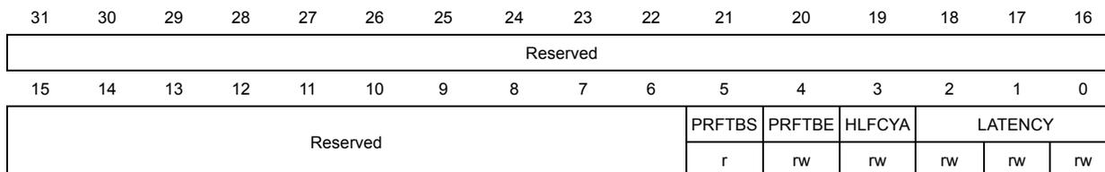
| 31 | 30 | 29 | 28 | 27 | 26 | 25 | 24 | 23 | 22 | 21 | 20 | 19 | 18 | 17 | 16 |
| Reserved | |||||||||||||||
| 15 | 14 | 13 | 12 | 11 | 10 | 9 | 8 | 7 | 6 | 5 | 4 | 3 | 2 | 1 | 0 |
| Reserved | PRFTBS | PRFTBE | HLFCYA | LATENCY | |||||||||||
| r | rw | rw | rw | rw | rw | ||||||||||
Bits 31:6 Reserved, must be kept at reset value.
Bit 5
PRFTBS
: Prefetch buffer status
This bit provides the status of the prefetch buffer.
0: Prefetch buffer is disabled
1: Prefetch buffer is enabled
Bit 4
PRFTBE
: Prefetch buffer enable
0: Prefetch is disabled
1: Prefetch is enabled
Bit 3
HLFCYA
: Flash half cycle access enable
0: Half cycle is disabled
1: Half cycle is enabled
Bits 2:0 LATENCY : Latency
These bits represent the ratio of the SYSCLK (system clock) period to the Flash access time.
000 Zero wait state, if
\(
0 < \text{SYSCLK} \leq 24 \text{ MHz}
\)
001 One wait state, if
\(
24 \text{ MHz} < \text{SYSCLK} \leq 48 \text{ MHz}
\)
010 Two wait states, if
\(
48 \text{ MHz} < \text{SYSCLK} \leq 72 \text{ MHz}
\)
3.4 Boot configuration
In the STM32F10xxx, 3 different boot modes can be selected through BOOT[1:0] pins as shown in Table 9 .
Table 9. Boot modes
| Boot mode selection pins | Boot mode | Aliasing | |
|---|---|---|---|
| BOOT1 | BOOT0 | ||
| x | 0 | Main Flash memory | Main Flash memory is selected as boot space |
| 0 | 1 | System memory | System memory is selected as boot space |
| 1 | 1 | Embedded SRAM | Embedded SRAM is selected as boot space |
The values on the BOOT pins are latched on the 4th rising edge of SYSCLK after a reset. It is up to the user to set the BOOT1 and BOOT0 pins after Reset to select the required boot mode.
The BOOT pins are also re-sampled when exiting from Standby mode. Consequently they must be kept in the required Boot mode configuration in Standby mode. After this startup delay has elapsed, the CPU fetches the top-of-stack value from address 0x0000 0000, then starts code execution from the boot memory starting from 0x0000 0004.
Due to its fixed memory map, the code area starts from address 0x0000 0000 (accessed through the ICode/DCode buses) while the data area (SRAM) starts from address 0x2000 0000 (accessed through the system bus). The Cortex®-M3 CPU always fetches the reset vector on the ICode bus, which implies to have the boot space available only in the code area (typically, Flash memory). STM32F10xxx microcontrollers implement a special mechanism to be able to boot also from SRAM and not only from main Flash memory and System memory.
Depending on the selected boot mode, main Flash memory, system memory or SRAM is accessible as follows:
- • Boot from main Flash memory: the main Flash memory is aliased in the boot memory space (0x0000 0000), but still accessible from its original memory space (0x800 0000). In other words, the Flash memory contents can be accessed starting from address 0x0000 0000 or 0x800 0000.
- • Boot from system memory: the system memory is aliased in the boot memory space (0x0000 0000), but still accessible from its original memory space (0x1FFF B000 in connectivity line devices, 0x1FFF F000 in other devices).
- • Boot from the embedded SRAM: SRAM is accessible only at address 0x2000 0000.
Note: When booting from SRAM, in the application initialization code, you have to relocate the vector table in SRAM using the NVIC exception table and offset register.
For XL-density devices, when booting from the main Flash memory, you have an option to boot from any of two memory banks. By default, boot from Flash memory bank 1 is selected. You can choose to boot from Flash memory bank 2 by clearing the BFB2 bit in the user option bytes. When this bit is cleared and the boot pins are in the boot from main Flash memory configuration, the device boots from system memory, and the boot loader jumps to execute the user application programmed in Flash memory bank 2. For further details refer to AN2606.
Note: When booting from Bank2 in the applications initialization code, relocate the vector table to the Bank2 base address. (0x0808 0000) using the NVIC exception table and offset register.
Embedded boot loader
The embedded boot loader is located in the System memory, programmed by ST during production. It is used to reprogram the Flash memory with one of the available serial interfaces:
- • In low-, medium- and high-density devices the boot loader is activated through the USART1 interface.
- • In XL-density devices the boot loader is activated through the following interfaces: USART1 or USART2 (remapped).
- • In connectivity line devices the boot loader can be activated through one of the following interfaces: USART1, USART2 (remapped), CAN2 (remapped) or USB OTG FS in Device mode (DFU: device firmware upgrade).
The USART peripheral operates with the internal 8 MHz oscillator (HSI). The CAN and USB OTG FS, however, can only function if an external 8 MHz, 14.7456 MHz or 25 MHz clock (HSE) is present.
Note: For further details refer to AN2606.